
High-Efficiency Metamaterial-Engineered Grating Couplers for Silicon Nitride Photonics
 , and
, and 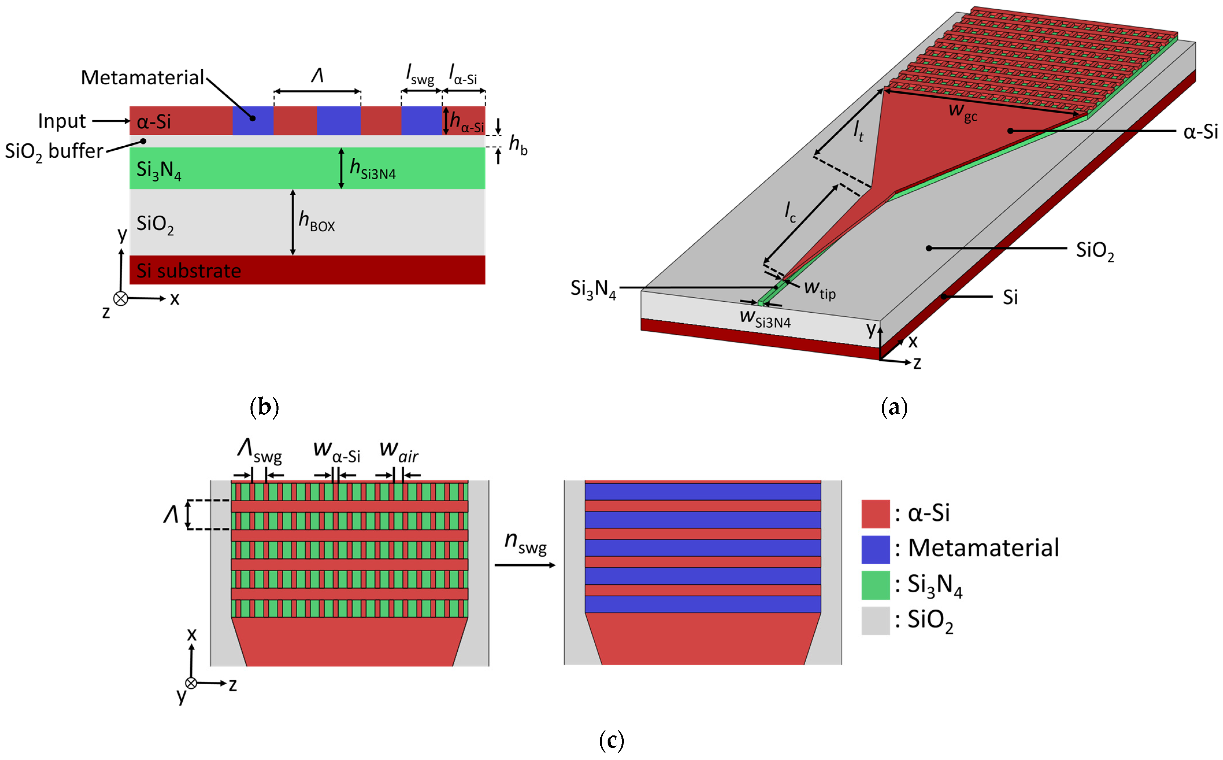
Abstract
:1. Introduction
2. Design and Methodology
2.1. Operating Principle and Performance
2.2. Material Platform Description
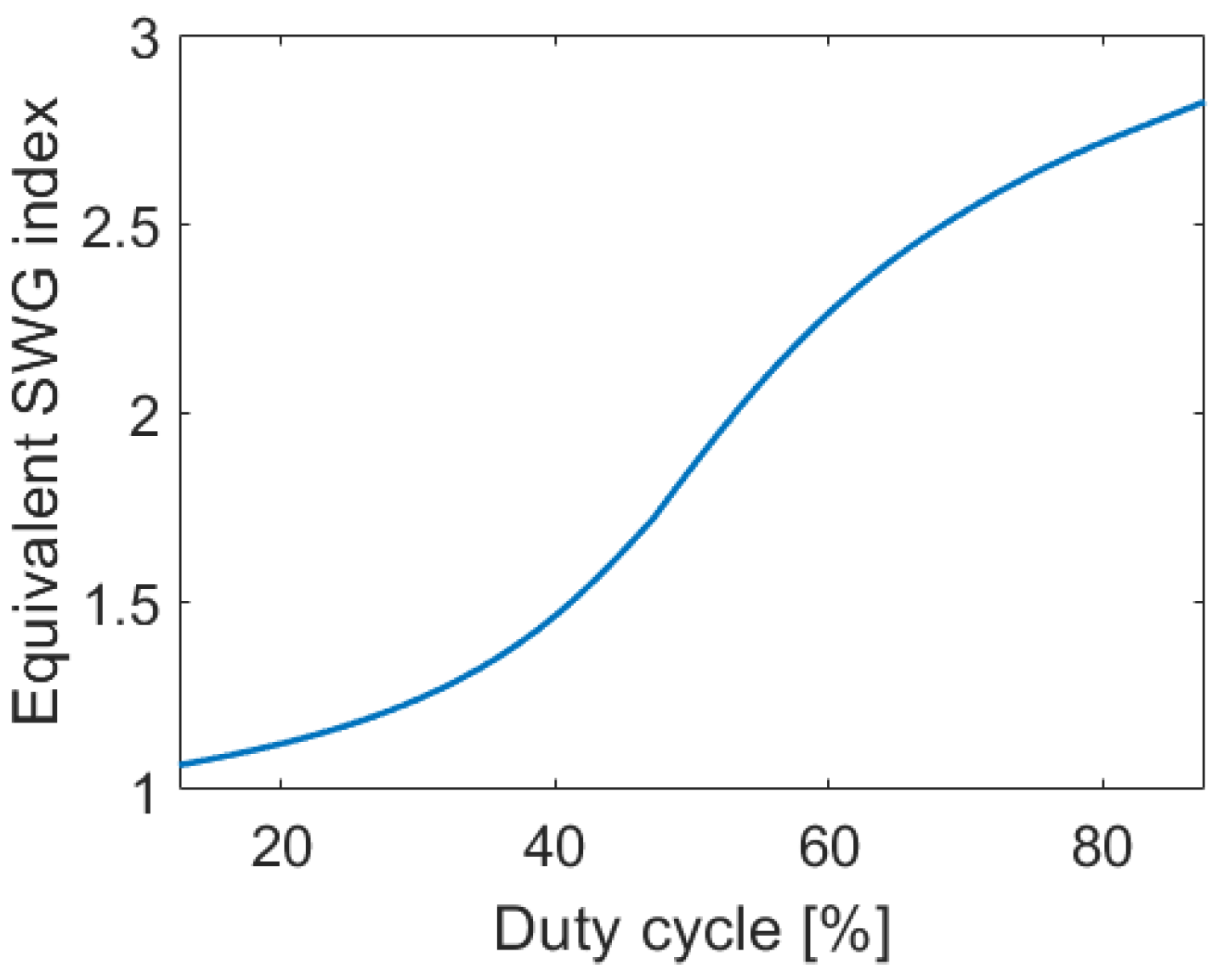
2.3. SWG Metamaterials
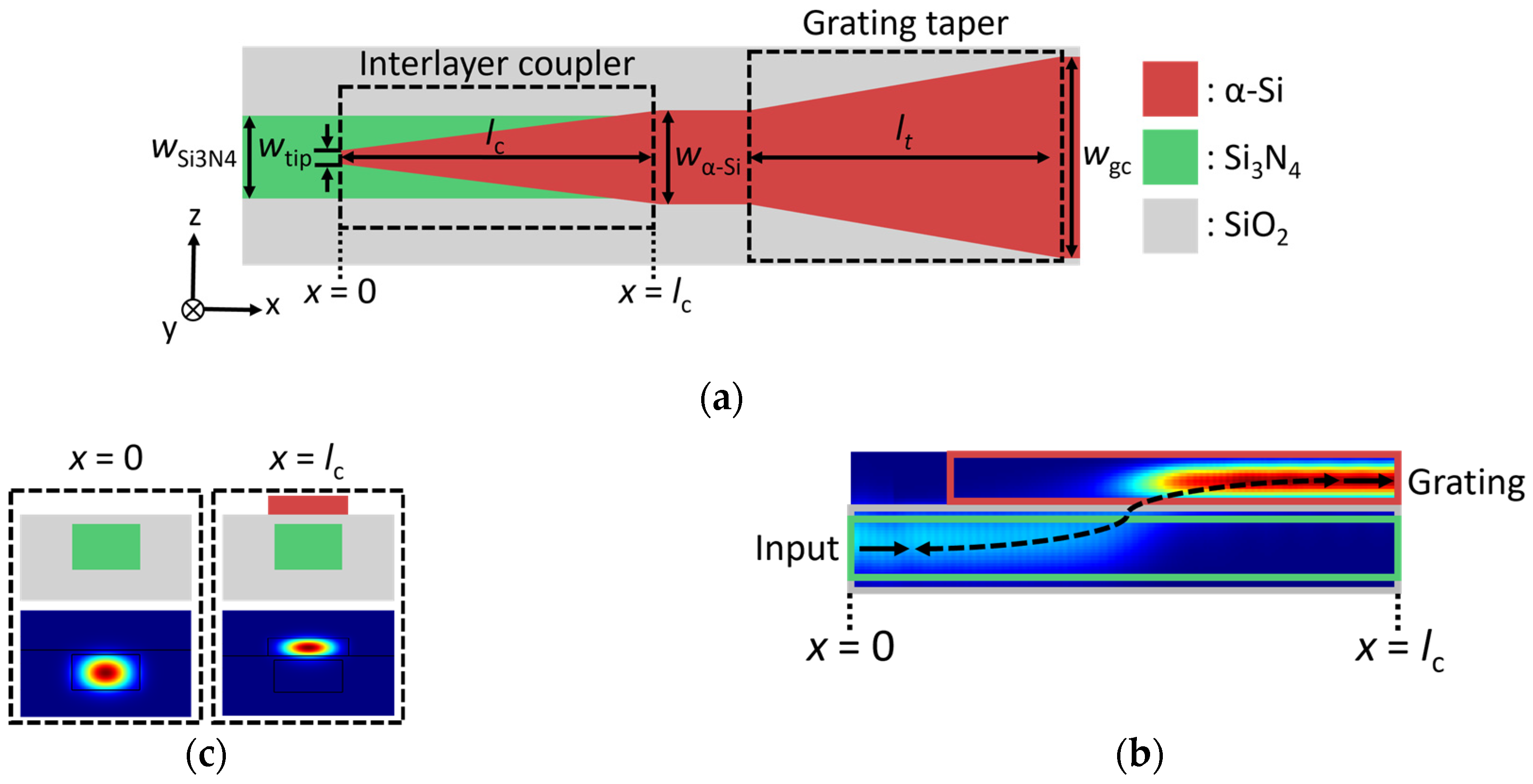
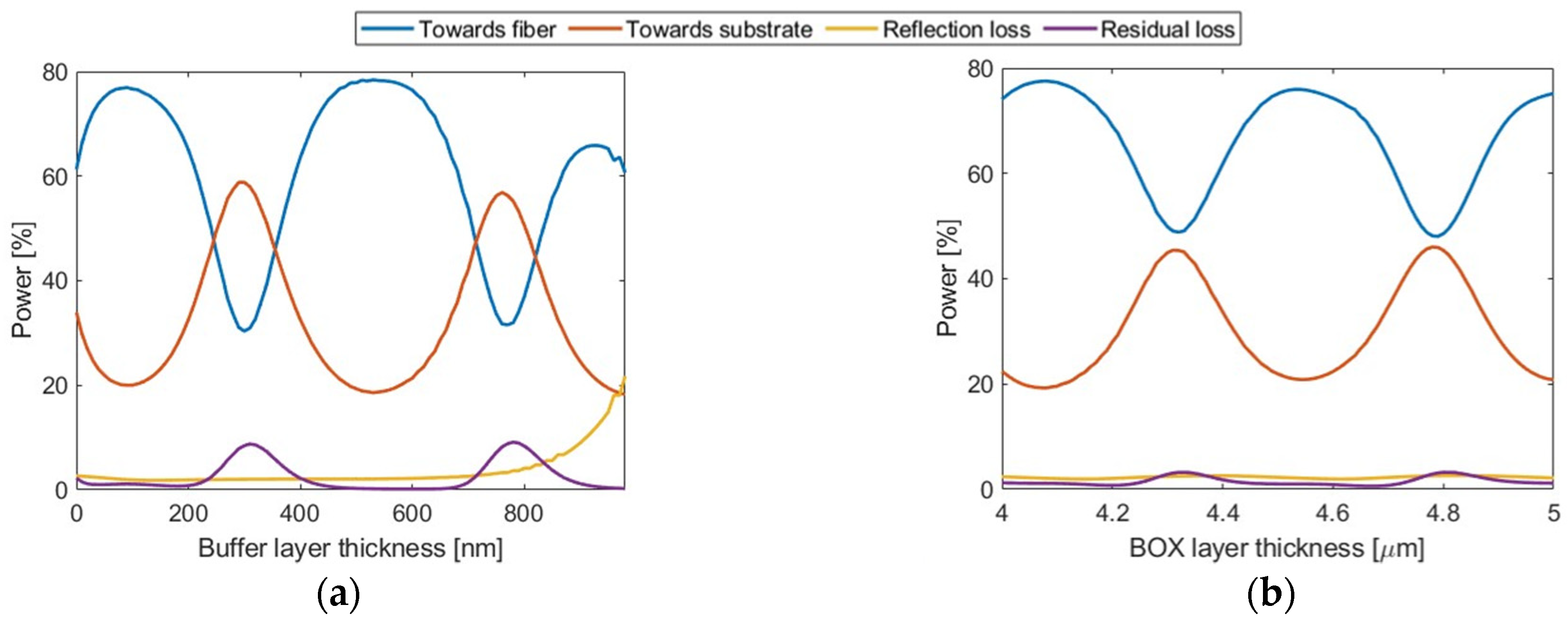
2.4. Connecting Waveguides and Inter-Layer Coupler
3. Results and Discussion
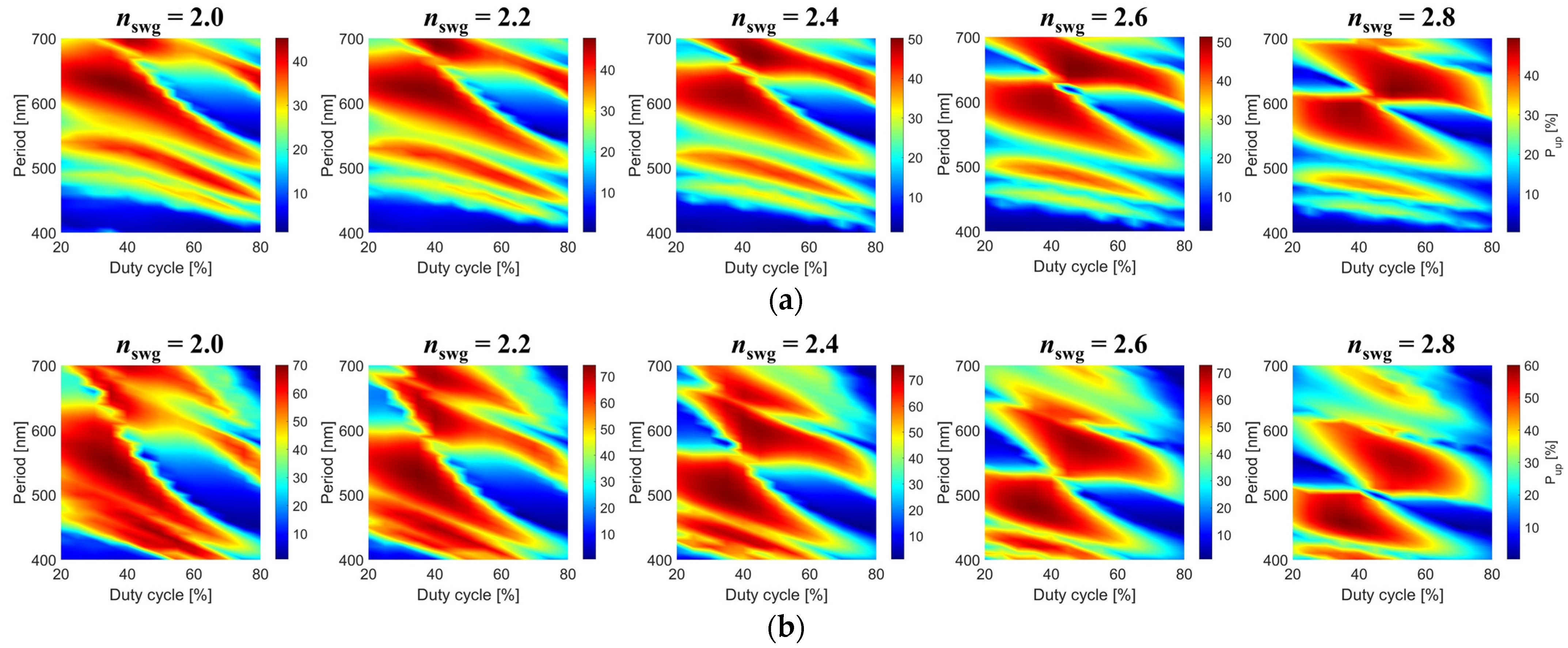
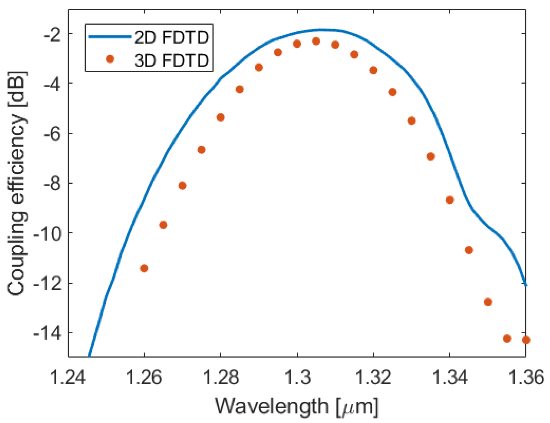
3.1. Uniform Grating Coupler
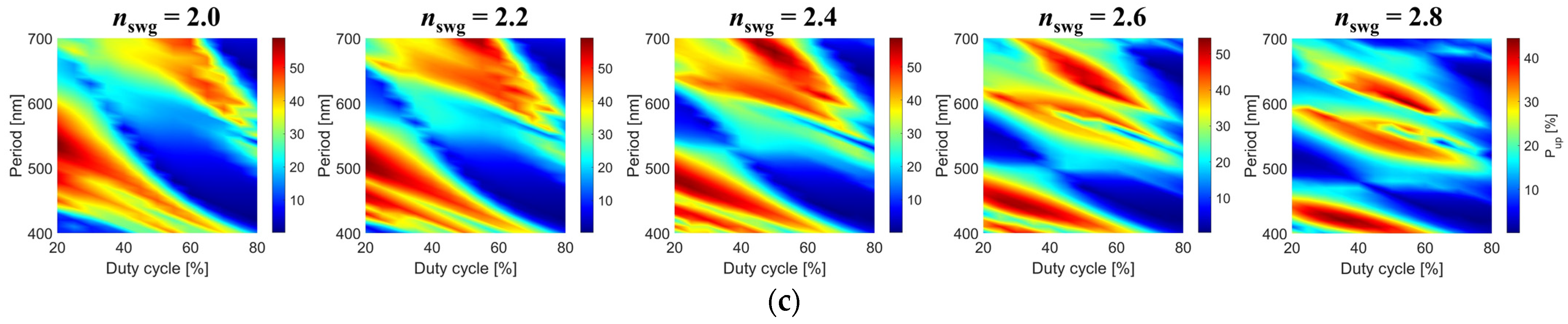
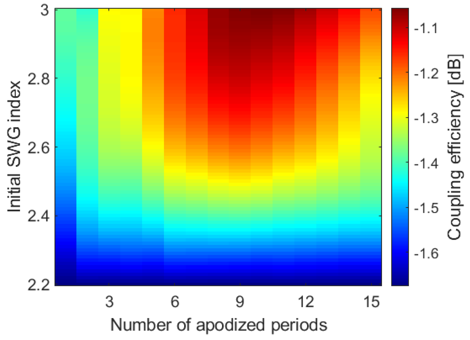
3.2. Apodized Grating Coupler
4. Conclusions
Author Contributions
Funding
Data Availability Statement
Conflicts of Interest
References
- Li, Y.; Zhang, Y.; Zhang, L.; Poon, A.W. Silicon and Hybrid Silicon Photonic Devices for Intra-Datacenter Applications: State of the Art and Perspectives. Photonics Res. 2015, 3, B10–B27. [Google Scholar] [CrossRef]
- Yoo, S.J. Ben Hybrid Integrated Photonic Platforms: Opinion. Opt. Mater. Express 2021, 11, 3528–3534. [Google Scholar] [CrossRef]
- Luo, W.; Cao, L.; Shi, Y.; Wan, L.; Zhang, H.; Li, S.; Chen, G.; Li, Y.; Li, S.; Wang, Y.; et al. Recent Progress in Quantum Photonic Chips for Quantum Communication and Internet. Light Sci. Appl. 2023, 12, 175. [Google Scholar] [CrossRef] [PubMed]
- Tran, M.A.; Zhang, C.; Morin, T.J.; Chang, L.; Barik, S.; Yuan, Z.; Lee, W.; Kim, G.; Malik, A.; Zhang, Z.; et al. Extending the Spectrum of Fully Integrated Photonics to Submicrometre Wavelengths. Nature 2022, 610, 54–60. [Google Scholar] [CrossRef] [PubMed]
- Chanana, A.; Larocque, H.; Moreira, R.; Carolan, J.; Guha, B.; Melo, E.G.; Anant, V.; Song, J.; Englund, D.; Blumenthal, D.J.; et al. Ultra-Low Loss Quantum Photonic Circuits Integrated with Single Quantum Emitters. Nat. Commun. 2022, 13, 7693. [Google Scholar] [CrossRef] [PubMed]
- Xiang, C.; Jin, W.; Bowers, J.E. Silicon Nitride Passive and Active Photonic Integrated Circuits: Trends and Prospects. Photonics Res. 2022, 10, A82. [Google Scholar] [CrossRef]
- Xiang, C.; Guo, J.; Jin, W.; Wu, L.; Peters, J.; Xie, W.; Chang, L.; Shen, B.; Wang, H.; Yang, Q.-F.; et al. High-Performance Lasers for Fully Integrated Silicon Nitride Photonics. Nat. Commun. 2021, 12, 6650. [Google Scholar] [CrossRef]
- Wei, W.-Q.; He, A.; Yang, B.; Wang, Z.-H.; Huang, J.-Z.; Han, D.; Ming, M.; Guo, X.; Su, Y.; Zhang, J.-J.; et al. Monolithic Integration of Embedded III-V Lasers on SOI. Light Sci. Appl. 2023, 12, 84. [Google Scholar] [CrossRef]
- Smith, J.A.; Jevtics, D.; Guilhabert, B.; Dawson, M.D.; Strain, M.J. Hybrid Integration of Chipscale Photonic Devices Using Accurate Transfer Printing Methods. Appl. Phys. Rev. 2022, 9, 041317. [Google Scholar] [CrossRef]
- Jimenez Gordillo, O.A.; Chaitanya, S.; Chang, Y.-C.; Dave, U.D.; Mohanty, A.; Lipson, M. Plug-and-Play Fiber to Waveguide Connector. Opt. Express 2019, 27, 20305–20310. [Google Scholar] [CrossRef]
- Marchetti, R.; Lacava, C.; Carroll, L.; Gradkowski, K.; Minzioni, P. Coupling Strategies for Silicon Photonics Integrated Chips. Photonics Res. 2019, 7, 201–239. [Google Scholar] [CrossRef]
- Papes, M.; Cheben, P.; Benedikovic, D.; Schmid, J.H.; Pond, J.; Halir, R.; Ortega-Moñux, A.; Wangüemert-Pérez, G.; Ye, W.N.; Xu, D.-X.; et al. Fiber-Chip Edge Coupler with Large Mode Size for Silicon Photonic Wire Waveguides. Opt. Express 2016, 24, 5026–5038. [Google Scholar] [CrossRef] [PubMed]
- Barwicz, T.; Peng, B.; Leidy, R.; Janta-Polczynski, A.; Houghton, T.; Khater, M.; Kamlapurkar, S.; Engelmann, S.; Fortier, P.; Boyer, N.; et al. Integrated Metamaterial Interfaces for Self-Aligned Fiber-to-Chip Coupling in Volume Manufacturing. IEEE J. Sel. Top. Quantum Electron. 2019, 25, 1–13. [Google Scholar] [CrossRef]
- Mu, X.; Wu, S.; Cheng, L.; Fu, H.Y. Edge Couplers in Silicon Photonic Integrated Circuits: A Review. Appl. Sci. 2020, 10, 1538. [Google Scholar] [CrossRef]
- Corning SMF-28 Ultra Optical Fibers. Available online: https://www.corning.com/optical-communications/worldwide/en/home/products/fiber/optical-fiber-products/smf-28-ultra.html (accessed on 21 August 2023).
- Korček, R.; Cheben, P.; Fraser, W.; Schmid, J.H.; Milanizadeh, M.; Alonso-Ramos, C.; Ye, W.N.; Benedikovič, D. Low-Loss Grating Coupler Based on Inter-Layer Mode Interference in a Hybrid Silicon Nitride Platform. Opt. Lett. 2023, 48, 4017–4020. [Google Scholar] [CrossRef]
- Mirshafiei, M.; Bérubé, J.-P.; Lessard, S.; Vallée, R.; Plant, D.V. Glass Interposer for Short Reach Optical Connectivity. Opt. Express 2016, 24, 12375–12384. [Google Scholar] [CrossRef] [PubMed]
- Poulton, C.V.; Yaacobi, A.; Cole, D.B.; Byrd, M.J.; Raval, M.; Vermeulen, D.; Watts, M.R. Coherent solid-state LIDAR with silicon photonic optical phased arrays. Opt. Lett. 2017, 42, 4091–4094. [Google Scholar] [CrossRef] [PubMed]
- Vermeulen, D.; Poulton, C.V. Optical Interfaces for Silicon Photonic Circuits. Proc. IEEE 2018, 106, 2270–2280. [Google Scholar] [CrossRef]
- Vivien, L.; Pavesi, L. Handbook of Silicon Photonics; CRC Press: Boca Raton, FL, USA, 2013. [Google Scholar]
- Chrostowski, L.; Hochberg, M. Silicon Photonics Design: From Devices to Systems; Cambridge University Press: Cambridge, UK, 2015. [Google Scholar]
- Bucio, T.D.; Lacava, C.; Clementi, M.; Faneca, J.; Skandalos, I.; Baldycheva, A.; Galli, M.; Debnath, K.; Petropoulos, P.; Gardes, F. Silicon Nitride Photonics for the Near-Infrared. IEEE J. Sel. Top. Quantum Electron. 2020, 26, 8200613. [Google Scholar] [CrossRef]
- Gardes, F.; Shooa, A.; De Paoli, G.; Skandalos, I.; Ilie, S.; Rutirawut, T.; Talataisong, W.; Faneca, J.; Vitali, V.; Hou, Y.; et al. A Review of Capabilities and Scope for Hybrid Integration Offered by Silicon-Nitride-Based Photonic Integrated Circuits. Sensors 2022, 22, 4227. [Google Scholar] [CrossRef]
- Tamir, T.; Peng, S.T. Analysis and Design of Grating Couplers. Appl. Phys. 1977, 14, 235–254. [Google Scholar] [CrossRef]
- Li, C.; Zhang, H.; Yu, M.; Lo, G.Q. CMOS-Compatible High Efficiency Double-Etched Apodized Waveguide Grating Coupler. Opt. Express 2013, 21, 7868. [Google Scholar] [CrossRef]
- Chen, X.; Tsang, H.K. Nanoholes Grating Couplers for Coupling Between Silicon-on-Insulator Waveguides and Optical Fibers. IEEE Photonics J. 2009, 1, 184–190. [Google Scholar] [CrossRef]
- Korček, R.; Medina Quiroz, D.; Wilmart, Q.; Edmond, S.; Cheben, P.; Vivien, L.; Alonso-Ramos, C.; Benedikovič, D. Library of Single-Etch Silicon Nitride Grating Couplers for Low-Loss and Fabrication-Robust Fiber-Chip Interconnection. Sci. Rep. 2023, 13, 17467. [Google Scholar] [CrossRef] [PubMed]
- Lomonte, E.; Stappers, M.; Krämer, L.; Pernice, W.H.P.; Lenzini, F. Scalable and Efficient Grating Couplers on Low-Index Photonic Platforms Enabled by Cryogenic Deep Silicon Etching. Sci. Rep. 2024, 14, 4256. [Google Scholar] [CrossRef] [PubMed]
- Oton, C.J. Long-Working-Distance Grating Coupler for Integrated Optical Devices. IEEE Photonics J. 2016, 8, 2700208. [Google Scholar] [CrossRef]
- Cheng, L.; Mao, S.; Li, Z.; Han, Y.; Fu, H.Y. Grating Couplers on Silicon Photonics: Design Principles, Emerging Trends and Practical Issues. Micromachines 2020, 11, 666. [Google Scholar] [CrossRef]
- Lim, A.E.-J.; Song, J.; Fang, Q.; Li, C.; Tu, X.; Duan, N.; Chen, K.K.; Tern, R.P.-C.; Liow, T.-Y. Review of Silicon Photonics Foundry Efforts. IEEE J. Sel. Top. Quantum Electron. 2014, 20, 405–416. [Google Scholar] [CrossRef]
- Zhao, X.; Li, D.; Zeng, C.; Gao, G.; Huang, Z.; Huang, Q.; Wang, Y.; Xia, J. Compact Grating Coupler for 700-Nm Silicon Nitride Strip Waveguides. J. Light. Technol. 2016, 34, 1322–1327. [Google Scholar] [CrossRef]
- Siew, S.Y.; Li, B.; Gao, F.; Zheng, H.Y.; Zhang, W.; Guo, P.; Xie, S.W.; Song, A.; Dong, B.; Luo, L.W.; et al. Review of Silicon Photonics Technology and Platform Development. J. Light. Technol. 2021, 39, 4374–4389. [Google Scholar] [CrossRef]
- Applied Nanotools Inc. Available online: https://www.appliednt.com/ (accessed on 1 November 2023).
- Romero-García, S.; Merget, F.; Zhong, F.; Finkelstein, H.; Witzens, J. Visible Wavelength Silicon Nitride Focusing Grating Coupler with AlCu/TiN Reflector. Opt. Lett. 2013, 38, 2521–2523. [Google Scholar] [CrossRef] [PubMed]
- Benedikovic, D.; Cheben, P.; Schmid, J.H.; Xu, D.-X.; Lamontagne, B.; Wang, S.; Lapointe, J.; Halir, R.; Ortega-Moñux, A.; Janz, S.; et al. Subwavelength Index Engineered Surface Grating Coupler with Sub-Decibel Efficiency for 220-Nm Silicon-on-Insulator Waveguides. Opt. Express 2015, 23, 22628–22635. [Google Scholar] [CrossRef] [PubMed]
- Zou, J.; Yu, Y.; Ye, M.; Liu, L.; Deng, S.; Zhang, X. Ultra Efficient Silicon Nitride Grating Coupler with Bottom Grating Reflector. Opt. Express 2015, 23, 26305–26312. [Google Scholar] [CrossRef] [PubMed]
- Nambiar, S.; Ranganath, P.; Kallega, R.; Selvaraja, S.K. High Efficiency DBR Assisted Grating Chirp Generators for Silicon Nitride Fiber-Chip Coupling. Sci. Rep. 2019, 9, 18821. [Google Scholar] [CrossRef] [PubMed]
- Hong, J.; Spring, A.M.; Qiu, F.; Yokoyama, S. A High Efficiency Silicon Nitride Waveguide Grating Coupler with a Multilayer Bottom Reflector. Sci. Rep. 2019, 9, 12988. [Google Scholar] [CrossRef]
- Chen, X.; Thomson, D.J.; Crudginton, L.; Khokhar, A.Z.; Reed, G.T. Dual-etch apodised grating couplers for efficient fibre-chip coupling near 1310 nm wavelength. Opt. Express 2017, 25, 17864–17871. [Google Scholar] [CrossRef]
- Watanabe, T.; Ayata, M.; Koch, U.; Fedoryshyn, Y.; Leuthold, J. Perpendicular Grating Coupler Based on a Blazed Antiback-Reflection Structure. J. Light. Technol. 2017, 35, 4663–4669. [Google Scholar] [CrossRef]
- Benedikovic, D.; Alonso-Ramos, C.; Guerber, S.; Le Roux, X.; Cheben, P.; Dupré, C.; Szelag, B.; Fowler, D.; Cassan, É.; Marris-Morini, D.; et al. Sub-Decibel Silicon Grating Couplers Based on L-Shaped Waveguides and Engineered Subwavelength Metamaterials. Opt. Express 2019, 27, 26239–26250. [Google Scholar] [CrossRef]
- Guo, R.; Zhang, S.; Gao, H.; Senthil Murugan, G.; Liu, T.; Cheng, Z. Blazed Subwavelength Grating Coupler. Photonics Res. 2023, 11, 189–195. [Google Scholar] [CrossRef]
- Notaros, J.; Pavanello, F.; Wade, M.T.; Gentry, C.M.; Atabaki, A.; Alloatti, L.; Ram, R.J.; Popović, M.A. Ultra-Efficient CMOS Fiber-to-Chip Grating Couplers. In Proceedings of the Optical Fiber Communication Conference; OSA: Washington, DC, USA, 2016; p. M2I.5. [Google Scholar]
- Michaels, A.; Yablonovitch, E. Inverse Design of near Unity Efficiency Perfectly Vertical Grating Couplers. Opt. Express 2018, 26, 4766–4779. [Google Scholar] [CrossRef]
- Ong, E.W.; Fahrenkopf, N.M.; Coolbaugh, D.D. SiNx Bilayer Grating Coupler for Photonic Systems. OSA Contin. 2018, 1, 13–25. [Google Scholar] [CrossRef]
- Roelkens, G.; Van Thourhout, D.; Baets, R. High Efficiency Silicon-on-Insulator Grating Coupler Based on a Poly-Silicon Overlay. Opt. Express 2006, 14, 11622–11630. [Google Scholar] [CrossRef] [PubMed]
- Vermeulen, D.; Selvaraja, S.; Verheyen, P.; Lepage, G.; Bogaerts, W.; Absil, P.; Van Thourhout, D.; Roelkens, G. High-Efficiency Fiber-to-Chip Grating Couplers Realized Using an Advanced CMOS-Compatible Silicon-On-Insulator Platform. Opt. Express 2010, 18, 18278–18283. [Google Scholar] [CrossRef] [PubMed]
- Yang, S.; Zhang, Y.; Baehr-Jones, T.; Hochberg, M. High Efficiency Germanium-Assisted Grating Coupler. Opt. Express 2014, 22, 30607–30612. [Google Scholar] [CrossRef] [PubMed]
- Fowler, D.R.; Wilmart, Q.; Garcia, S.; Olivier, S.; Szelag, B. Fiber Grating Couplers for Optical Access via the Chip Backside. J. Light. Technol. 2021, 39, 557–561. [Google Scholar] [CrossRef]
- Chmielak, B.; Suckow, S.; Parra, J.; Duarte, V.C.; Mengual, T.; Piqueras, M.A.; Giesecke, A.L.; Lemme, M.C.; Sanchis, P. High-Efficiency Grating Coupler for an Ultralow-Loss Si3N4-Based Platform. Opt. Lett. 2022, 47, 2498–2501. [Google Scholar] [CrossRef] [PubMed]
- Mak, J.C.C.; Sacher, W.D.; Ying, H.; Luo, X.; Lo, P.G.-Q.; Poon, J.K.S. Multi-Layer Silicon Nitride-on-Silicon Polarization-Independent Grating Couplers. Opt. Express 2018, 26, 30623–30633. [Google Scholar] [CrossRef]
- Vitali, V.; Lacava, C.; Domínguez Bucio, T.; Gardes, F.Y.; Petropoulos, P. Highly Efficient Dual-Level Grating Couplers for Silicon Nitride Photonics. Sci. Rep. 2022, 12, 15436. [Google Scholar] [CrossRef]
- Kohli, M.; Chelladurai, D.; Vukovic, B.; Moor, D.; Bisang, D.; Keller, K.; Messner, A.; Buriakova, T.; Zervas, M.; Fedoryshyn, Y.; et al. C- and O-Band Dual-Polarization Fiber-to-Chip Grating Couplers for Silicon Nitride Photonics. ACS Photonics 2023, 10, 3366–3373. [Google Scholar] [CrossRef]
- Cheng, L.; Mao, S.; Mu, X.; Wu, S.; Fu, H.Y. Dual-Wavelength-Band Multiplexed Grating Coupler on Multilayer SiN-on-SOI Photonic Integrated Platform. In Proceedings of the Conference on Lasers and Electro-Optics; Optica Publishing Group: Washington, DC, USA, 2020; pp. 1–2. [Google Scholar]
- Kohli, M.; Chelladurai, D.; Buriakova, T.; Moor, D.; Eppenberger, M.; Zervas, M.; Fedoryshyn, Y.; Koch, U.; Leuthold, J. Efficient Polarization-Insensitive O-Band Grating Couplers for Silicon Nitride. In Proceedings of the Optica Advanced Photonics Congress 2022, Maastricht, The Netherlands, 24–28 July 2022. [Google Scholar]
- Cao, L.; Aboketaf, A.; Wang, Z.; Preble, S. Hybrid Amorphous Silicon (a-Si:H)–LiNbO3 Electro-Optic Modulator. Opt. Commun. 2014, 330, 40–44. [Google Scholar] [CrossRef]
- Kang, J.; Takagi, S.; Takenaka, M. Ge Photodetector Monolithically Integrated with Amorphous Si Waveguide on Wafer-Bonded Ge-on-Insulator Substrate. Opt. Express 2018, 26, 30546–30555. [Google Scholar] [CrossRef] [PubMed]
- Hosseinnia, A.H.; Atabaki, A.H.; Eftekhar, A.A.; Adibi, A. High-Quality Silicon on Silicon Nitride Integrated Optical Platform with an Octave-Spanning Adiabatic Interlayer Coupler. Opt. Express 2015, 23, 30297–30307. [Google Scholar] [CrossRef]
- Georgieva, G.; Mai, C.; Seiler, P.M.; Peczek, A.; Zimmermann, L. Dual-Polarization Multiplexing Amorphous Si:H Grating Couplers for Silicon Photonic Transmitters in the Photonic BiCMOS Backend of Line. Front. Optoelectron. 2022, 15, 13. [Google Scholar] [CrossRef]
- Cheben, P.; Halir, R.; Schmid, J.H.; Atwater, H.A.; Smith, D.R. Subwavelength Integrated Photonics. Nature 2018, 560, 565–572. [Google Scholar] [CrossRef] [PubMed]
- Ansys. Available online: https://www.ansys.com/ (accessed on 16 July 2023).
- Halir, R.; Ortega-Moñux, A.; Benedikovic, D.; Mashanovich, G.Z.; Wangüemert-Pérez, J.G.; Schmid, J.H.; Molina-Fernández, Í.; Cheben, P. Subwavelength-Grating Metamaterial Structures for Silicon Photonic Devices. Proc. IEEE 2018, 106, 2144–2157. [Google Scholar] [CrossRef]
- Cheben, P.; Schmid, J.H.; Halir, R.; Manuel Luque-González, J.; Gonzalo Wangüemert-Pérez, J.; Melati, D.; Alonso-Ramos, C. Recent Advances in Metamaterial Integrated Photonics. Adv. Opt. Photonics 2023, 15, 1033. [Google Scholar] [CrossRef]
- Benedikovic, D.; Berciano, M.; Alonso-Ramos, C.; Le Roux, X.; Cassan, E.; Marris-Morini, D.; Vivien, L. Dispersion Control of Silicon Nanophotonic Waveguides Using Sub-Wavelength Grating Metamaterials in near- and Mid-IR Wavelengths. Opt. Express 2017, 25, 19468–19478. [Google Scholar] [CrossRef]
- Dinh, T.T.D.; Le Roux, X.; Zhang, J.; Montesinos-Ballester, M.; Lafforgue, C.; Benedikovic, D.; Cheben, P.; Cassan, E.; Marris-Morini, D.; Vivien, L.; et al. Controlling the Modal Confinement in Silicon Nanophotonic Waveguides through Dual-Metamaterial Engineering. Laser Photon Rev. 2023, 17, 2100305. [Google Scholar] [CrossRef]
- Xu, H.; Dai, D.; Shi, Y. Ultra-Broadband and Ultra-Compact On-Chip Silicon Polarization Beam Splitter by Using Hetero-Anisotropic Metamaterials. Laser Photon Rev. 2019, 13, 1800349. [Google Scholar] [CrossRef]
- Fowler, D.; Grosse, P.; Gays, F.; Szelag, B.; Baudot, C.; Vuillet, N.; Planchot, J.; Boeuf, F. Fiber Grating Coupler Development for Si-Photonics Process Design Kits at CEA-LETI. In Proceedings of the Smart Photonic and Optoelectronic Integrated Circuits XXI; Lee, E.-H., He, S., Eds.; SPIE: Bellingham, WA, USA, 2019; p. 4. [Google Scholar]
- Zhang, C.; Sun, J.-H.; Xiao, X.; Sun, W.-M.; Zhang, X.-J.; Chu, T.; Yu, J.-Z.; Yu, Y.-D. High Efficiency Grating Coupler for Coupling between Single-Mode Fiber and SOI Waveguides. Chin. Phys. Lett. 2013, 30, 014207. [Google Scholar] [CrossRef]
- Vakarin, V.; Melati, D.; Dinh, T.T.D.; Le Roux, X.; Kan, W.K.K.; Dupré, C.; Szelag, B.; Monfray, S.; Boeuf, F.; Cheben, P.; et al. Metamaterial-Engineered Silicon Beam Splitter Fabricated with Deep UV Immersion Lithography. Nanomaterials 2021, 11, 2949. [Google Scholar] [CrossRef] [PubMed]


Disclaimer/Publisher’s Note: The statements, opinions and data contained in all publications are solely those of the individual author(s) and contributor(s) and not of MDPI and/or the editor(s). MDPI and/or the editor(s) disclaim responsibility for any injury to people or property resulting from any ideas, methods, instructions or products referred to in the content. |
© 2024 by the authors. Licensee MDPI, Basel, Switzerland. This article is an open access article distributed under the terms and conditions of the Creative Commons Attribution (CC BY) license (https://creativecommons.org/licenses/by/4.0/).
Share and Cite
Fraser, W.; Korček, R.; Glesk, I.; Litvik, J.; Schmid, J.H.; Cheben, P.; Ye, W.N.; Benedikovic, D. High-Efficiency Metamaterial-Engineered Grating Couplers for Silicon Nitride Photonics. Nanomaterials 2024, 14, 581. https://0-doi-org.brum.beds.ac.uk/10.3390/nano14070581
Fraser W, Korček R, Glesk I, Litvik J, Schmid JH, Cheben P, Ye WN, Benedikovic D. High-Efficiency Metamaterial-Engineered Grating Couplers for Silicon Nitride Photonics. Nanomaterials. 2024; 14(7):581. https://0-doi-org.brum.beds.ac.uk/10.3390/nano14070581
Chicago/Turabian StyleFraser, William, Radovan Korček, Ivan Glesk, Jan Litvik, Jens H. Schmid, Pavel Cheben, Winnie N. Ye, and Daniel Benedikovic. 2024. "High-Efficiency Metamaterial-Engineered Grating Couplers for Silicon Nitride Photonics" Nanomaterials 14, no. 7: 581. https://0-doi-org.brum.beds.ac.uk/10.3390/nano14070581