Angle-Selective Photodetection in Ge/Si Quantum Dot Photodiodes Enhanced by Microstructured Hole Arrays

 , , , and
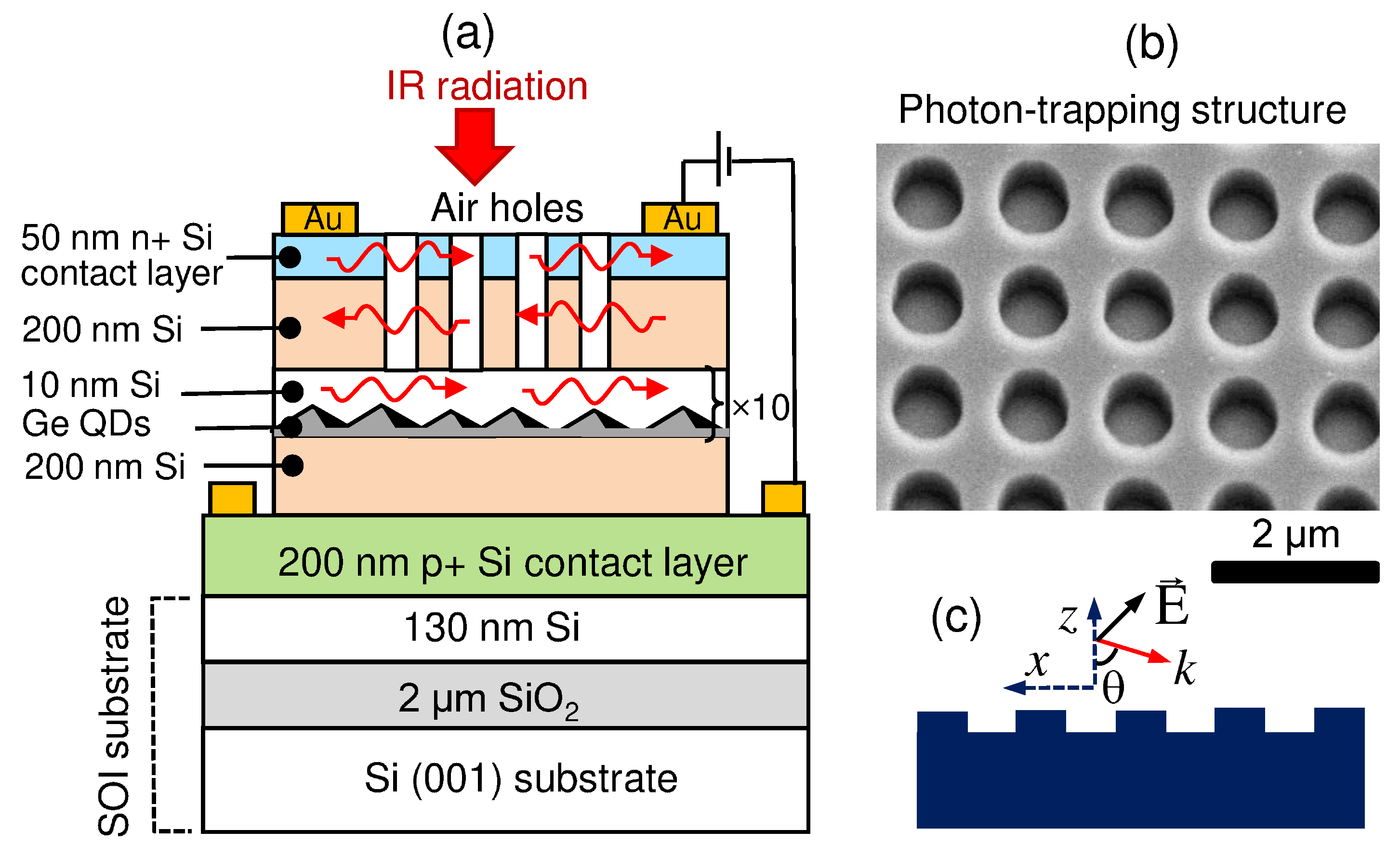
Abstract
:1. Introduction
2. Materials and Methods
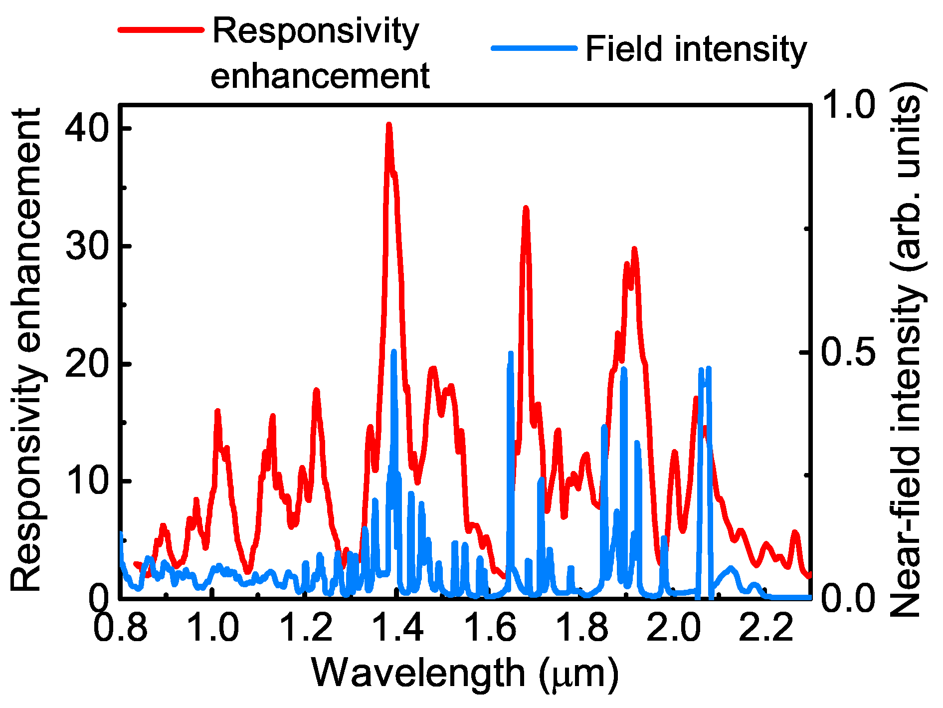
3. Results and Discussion
4. Conclusions
Author Contributions
Funding
Institutional Review Board Statement
Informed Consent Statement
Data Availability Statement
Acknowledgments
Conflicts of Interest
References
- Li, W.G.; Wang, X.D.; Liao, J.F.; Jiang, Y.; Kuang, D.B. Enhanced on-off ratio photodetectors based on lead-free Cs3Bi2I9 single crystal thin films. Adv. Funct. Mater. 2020, 30, 1909701. [Google Scholar] [CrossRef]
- Song, W.; Chen, J.; Li, Z.; Fang, X. Self-powered MXene/GaN van der Waals heterojunction ultraviolet photodiodes with superhigh efficiency and stable current outputs. Adv. Mater. 2021, 33, 2101059. [Google Scholar] [CrossRef]
- Han, S.; Quan, J.; Wang, D.; Li, H.; Liu, X.; Xu, J.; Zhang, Y.; Li, Z.; Wu, L.; Fang, X. Anisotropic growth of centimeter-size CsCu2I3 single crystals with ultra-low trap density for aspect-ratio-dependent photodetectors. Adv. Sci. 2023, 10, 2206417. [Google Scholar] [CrossRef] [PubMed]
- Tong, J.; Suo, F.; Ma, J.; Tobing, L.; Qian, L.; Zhang, D. Surface plasmon enhanced infrared photodetection. Opto-Electron. Adv. 2019, 2, 180026. [Google Scholar] [CrossRef]
- Patra, A.; Rout, C.S. Self-Assembled Quantum Dot Photodetector: A Pathbreaker in the Field of Optoelectronics. In Quantum Dot Photodetectors; Tong, X., Wu, J., Wang, Z.M., Eds.; Springer: Cham, Switzerland, 2021; pp. 289–305. [Google Scholar]
- Hu, X.; Wu, J.; Wu, M.; Hu, J. Recent developments of infrared photodetectors with low-dimensional inorganic nanostructures. Nano Res. 2022, 15, 805–817. [Google Scholar] [CrossRef]
- Hao, Q.; Zhao, X.; Tang, X.; Chen, M. The historical development of infrared photodetection based on intraband transitions. Materials 2023, 16, 1562. [Google Scholar] [CrossRef]
- Guo, H.; Qi, W. New materials and designs for 2D-based infrared photodetectors. Nano Res. 2023, 16, 3074–3103. [Google Scholar] [CrossRef]
- Yan, N.; Qiu, Y.; He, X.; Tang, X.; Hao, Q.; Chen, M. Plasmonic enhanced nanocrystal infrared photodetectors. Materials 2023, 16, 3216. [Google Scholar] [CrossRef]
- Paul, D. Si/SiGe heterostructures: From material and physics to devices and circuits. Semicond. Sci. Technol. 2004, 19, R75–R108. [Google Scholar] [CrossRef]
- Michel, J.; Liu, J.; Kimerling, L.C. High-performance Ge-on-Si photodetectors. Nat. Photonics 2010, 4, 527–534. [Google Scholar] [CrossRef]
- Sood, A.K.; Zeller, J.W.; Richwine, R.A.; Puri, Y.R.; Efsathiadis, H.; Haldar, P.; Dhar, N.K.; Polla, D.L. SiGe-based visible-NIR photodetector technology for optoelectronic applications. In Advances in Optical Fiber Technology: Fundamental Optical Phenomena and Applications; Yasin, M., Arof, H., Harun, S.W., Eds.; Intech: Rijeka, Croatia, 2015; pp. 315–362. [Google Scholar]
- Douhan, R.; Lozovoy, K.; Kokhanenko, A.; Deeb, H.; Dirko, V.; Khomyakova, K. Recent advances in Si-compatible nanostructured photodetectors. Technologies 2023, 11, 17. [Google Scholar] [CrossRef]
- Tong, S.; Liu, J.; Wang, J.; Wang, K. Normal-incidence Ge quantum-dot photodetectors at 1.5 μm based on Si substrate. Appl. Phys. Lett. 2002, 80, 1189–1191. [Google Scholar] [CrossRef]
- Alguno, A.; Usami, N.; Ujihara, T.; Fujiwara, K.; Sazaki, G.; Nakajima, K.; Shiraki, Y. Enhanced quantum efficiency of solar cells with self-assembled Ge dots stacked in multilayer structure. Appl. Phys. Lett. 2003, 83, 1258–1260. [Google Scholar] [CrossRef]
- Elfving, A.; Hansson, G.; Ni, W.X. SiGe (Ge-dot) heterojunction phototransistors for efficient light detection at 1.3–1.55 μm. Physica E 2003, 16, 528–532. [Google Scholar] [CrossRef]
- Yakimov, A.I.; Kirienko, V.V.; Armbrister, V.A.; Bloshkin, A.A.; Dvurechenskii, A.V. Photoconductive gain and quantum efficiency of remotely doped Ge/Si quantum dot photodetectors. Mater. Res. Express 2016, 3, 105032. [Google Scholar] [CrossRef]
- Brunner, K. Si/Ge nanostructures. Rep. Prog. Phys. 2002, 65, 27–72. [Google Scholar] [CrossRef]
- Schmidt, O.G.; Eberl, K.; Rau, Y. Strain and band-edge alignment in single and multiple layers of self-assembled Ge/Si and GeSi/Si islands. Phys. Rev. B 2000, 62, 16715–16720. [Google Scholar] [CrossRef]
- Grützmacher, D.; Fromherz, T.; Dais, C.; Stangl, J.; Müller, E.; Ekinci, Y.; Solak, H.; Sigg, H.; Lechner, R.; Wintersberger, E.; et al. Three-Dimensional Si/Ge Quantum Dot Crystals. Nano Lett. 2007, 7, 3150–3156. [Google Scholar] [CrossRef] [PubMed]
- Yakimov, A.I.; Kirienko, V.V.; Bloshkin, A.A.; Dvurechenskii, A.V.; Utkin, D.E. Near-infrared photoresponse in Ge/Si quantum dots enhanced by localized surface plasmons supported by aluminium nanodisks. J. Appl. Phys. 2020, 128, 143101. [Google Scholar] [CrossRef]
- Donnelly, J.L.; Sturmberg, B.C.; Dossou, K.B.; Botten, L.C.; Asatryan, A.A.; Poulton, C.G.; McPhedran, R.C.; de Sterke, M. Mode-based analysis of silicon nanohole arrays for photovoltaic applications. Opt. Express 2014, 22, A1343–A1354. [Google Scholar] [CrossRef] [Green Version]
- Gao, Y.; Cansizoglu, H.; Polat, K.G.; Ghandiparsi, S.; Kaya, A.; Mamtaz, H.H.; Mayet, A.S.; Wang, Y.; Zhang, X.; Yamada, T.; et al. Photon-trapping microstructures enable high-speed high-efficiency silicon photodiodes. Nat. Photonics 2017, 11, 301–309. [Google Scholar] [CrossRef]
- Cansizoglu, H.; Bartolo-Perez, C.; Gao, Y.; Ponizovskaya Devine, E.; Ghandiparsi, S.; Polat, K.G.; Mamtaz, H.H.; Yamada, T.; Elrefaie, A.F.; Wang, S.Y.; et al. Surface-illuminated photon-trapping high-speed Ge-on-Si photodiodes with improved efficiency up to 1700 nm. Photonics Res. 2018, 6, 734–742. [Google Scholar] [CrossRef]
- Ghandiparsi, S.; Elrefaie, A.F.; Mayet, A.S.; Landolsi, T.; Bartolo-Perez, C.; Cansizoglu, H.; Gao, Y.; Mamtaz, H.H.; Golgir, H.R.; Ponizovskaya Devine, E.; et al. High-speed high-efficiency pin photodiodes for short-reach optical interconnects in data centers. IEEE J. Light. Technol. 2019, 37, 5748–5755. [Google Scholar] [CrossRef]
- Zhou, H.; Xu, S.; Lin, Y.; Huang, Y.C.; Son, B.; Chen, Q.; Guo, X.; Lee, K.H.; Gon, S.C.K.; Gong, X.; et al. High-efficiency GeSn/Si multiple-quantum-well photodetectors with photon-trapping microstructures operating at 2 μm. Opt. Express 2020, 28, 10280–10293. [Google Scholar] [CrossRef] [PubMed]
- Cansizoglu, H.; Ponizovskaya Devine, E.; Gao, Y.; Ghandiparsi, S.; Yamada, T.; Elrefaie, A.F.; Wang, S.Y.; Islam, M.S. A new paradigm in high-speed and high-efficiency silicon photodiodes for communication – Part I: Enhancing photon-material interaction via low-dimensional structures. IEEE Trans. Electron Devices 2018, 65, 372–381. [Google Scholar] [CrossRef]
- Yamada, T.; Ponizovskaya Devine, E.; Ghandiparsi, S.; Bartolo-Perez, C.; Mayet, A.S.; Cansizoglu, H.; Gao, Y.; Ahamed, A.; Wang, S.Y.; Islam, M.S. Modeling of nanohole silicon pin/nip photodetectors: Steady state and transient characteristics. Nanotechnology 2021, 32, 365201. [Google Scholar] [CrossRef] [PubMed]
- Bartolo-Perez, C.; Chandiparsi, S.; Mayet, A.S.; Cansizoglu, H.; Gao, Y.; Qarony, W.; Ahamed, A.; Wang, S.Y.; Cherry, S.R.; Islam, M.S.; et al. Avalanche photodetectors with photon trapping structures for biomedical imaging applications. Opt. Express 2021, 29, 19024–19033. [Google Scholar] [CrossRef]
- Yakimov, A.I.; Kirienko, V.V.; Bloshkin, A.A.; Utkin, D.E.; Dvurechenskii, A.V. Near-infrared photoresponse in Ge/Si quantum dots enhanced by photon-trapping hole arrays. Nanomaterials 2021, 11, 2302. [Google Scholar] [CrossRef]
- Yakimov, A.I.; Kirienko, V.V.; Utkin, D.E.; Dvurechenskii, A.V. Light-trapping-enhanced photodetection in Ge/Si quantum dot photodiodes containing microhole arrays with different hole depths. Nanomaterials 2022, 12, 2993. [Google Scholar] [CrossRef]
- Ünlü, M.S.; Strite, S. Resonant cavity enhanced photonic devices. J. Appl. Phys. 1995, 78, 607–639. [Google Scholar] [CrossRef]
- Shen, Y.; Ye, D.; Celanovic, I.; Johnson, S.G.; Joannopoulos, J.D.; Soljačić, M.S. Optical broadband angular selectivity. Science 2014, 343, 1499–1501. [Google Scholar] [CrossRef] [Green Version]
- Kemsri, T.; Gu, G.; Zhang, Y.; Lan, X.; Zhang, H.; Tice, J.; Lu, X. Angular-dependent photodetection enhancement by a metallic circular disk optical antenna. AIP Adv. 2017, 7, 025013. [Google Scholar] [CrossRef] [Green Version]
- Yi, S.; Zhou, M.; Yu, Z.; Fan, P.; Behdad, N.; Lin, D.; Wang, K.X.; Fan, S.; Brongersma, M. Subwavelength angle-sensing photodetectors inspired by directional hearing in small animals. Nat. Nanotechnol. 2018, 13, 1143–1147. [Google Scholar] [CrossRef]
- Nagarajan, A.; Hara, S.; Satoh, H.; Panchanathan, A.P.; Inokawa, H. Angular selectivity of SOI photodiode with surface plasmon antenna. IEICE Electron. Express 2020, 17, 1–6. [Google Scholar] [CrossRef]
- Huang, C.H.; Wu, C.H.; Bikbaev, R.G.; Ye, M.J.; Chen, C.W.; Wang, T.J.; Timofeev, I.V.; Lee, W.; Chen, K.P. Wavelength- and angle-selective photodetectors enabled by graphene hot electrons with Tamm plasmon polaritons. Nanomaterials 2023, 13, 693. [Google Scholar] [CrossRef]
- Zang, K.; Jiang, X.; Huo, Y.; Ding, X.; Morea, M.; Chen, X.; Lu, C.Y.; Ma, J.; Zhou, M.; Xia, Z.; et al. Silicon single-photon avalanche diodes with nanostructured light trapping. Nat. Commun. 2017, 8, 628. [Google Scholar] [CrossRef] [PubMed] [Green Version]
- Suo, F.; Tong, J.; Zhang, D.H. Photon-trapping array for enhanced midwave infrared photoresponse. J. Phys. D Appl. Phys. 2021, 54, 505105. [Google Scholar] [CrossRef]
- Baba, T. Slow light in photonic crystals. Nat. Photonics 2008, 2, 465–473. [Google Scholar] [CrossRef]
- Duché, D.; Escoubas, L.; Simon, J.J.; Torchio, P.; Vervisch, W.; Flory, F. Slow Bloch modes for enhancing the absorption of light in thin films for photovoltaic cells. Appl. Phys. Lett. 2008, 92, 193310. [Google Scholar] [CrossRef]
- Sturmberg, B.C.; Dossou, K.B.; Botten, L.C.; Asatryan, A.A.; Poulton, C.G.; de Sterke, M.; McPhedran, R.C. Modal analysis of enhanced absorption in silicon nanowire arrays. Opt. Express 2011, 19, A1067–A1081. [Google Scholar] [CrossRef] [PubMed] [Green Version]
- Gomard, G.; Peretti, R.; Callard, S.; Meng, X.; Artinyan, R.; Deschamps, T.; i Cabarrocas, P.R.; Drouard, E.; Seassal, C. Blue light absorption enhancement based on vertically channeling modes in nano-hole arrays. Appl. Phys. Lett. 2014, 104, 051119. [Google Scholar] [CrossRef] [Green Version]
- Yakimov, A.I.; Bloshkin, A.A.; Dvurechenskii, A.V. Tailoring the optical field enhancement in Si-based structures covered by nanohole arrays in gold films for near-infrared photodetection. Photonics Nanostruct. 2020, 40, 100790. [Google Scholar] [CrossRef]
- Joannopoulos, J.D.; Johnson, S.G.; Winn, J.N.; Meade, R.D. Photonic Crystals: Molding the Flow of Light; Princeton University Press: Princeton, NJ, USA; Oxford, UK, 2008. [Google Scholar]


Disclaimer/Publisher’s Note: The statements, opinions and data contained in all publications are solely those of the individual author(s) and contributor(s) and not of MDPI and/or the editor(s). MDPI and/or the editor(s) disclaim responsibility for any injury to people or property resulting from any ideas, methods, instructions or products referred to in the content. |
© 2023 by the authors. Licensee MDPI, Basel, Switzerland. This article is an open access article distributed under the terms and conditions of the Creative Commons Attribution (CC BY) license (https://creativecommons.org/licenses/by/4.0/).
Share and Cite
Yakimov, A.I.; Kirienko, V.V.; Bloshkin, A.A.; Utkin, D.E.; Dvurechenskii, A.V. Angle-Selective Photodetection in Ge/Si Quantum Dot Photodiodes Enhanced by Microstructured Hole Arrays. Photonics 2023, 10, 764. https://0-doi-org.brum.beds.ac.uk/10.3390/photonics10070764
Yakimov AI, Kirienko VV, Bloshkin AA, Utkin DE, Dvurechenskii AV. Angle-Selective Photodetection in Ge/Si Quantum Dot Photodiodes Enhanced by Microstructured Hole Arrays. Photonics. 2023; 10(7):764. https://0-doi-org.brum.beds.ac.uk/10.3390/photonics10070764
Chicago/Turabian StyleYakimov, Andrew I., Victor V. Kirienko, Aleksei A. Bloshkin, Dmitrii E. Utkin, and Anatoly V. Dvurechenskii. 2023. "Angle-Selective Photodetection in Ge/Si Quantum Dot Photodiodes Enhanced by Microstructured Hole Arrays" Photonics 10, no. 7: 764. https://0-doi-org.brum.beds.ac.uk/10.3390/photonics10070764