Investigation of Side Wall Roughness Effect on Optical Losses in a Multimode Si3N4 Waveguide Formed on a Quartz Substrate

Abstract
:1. Introduction
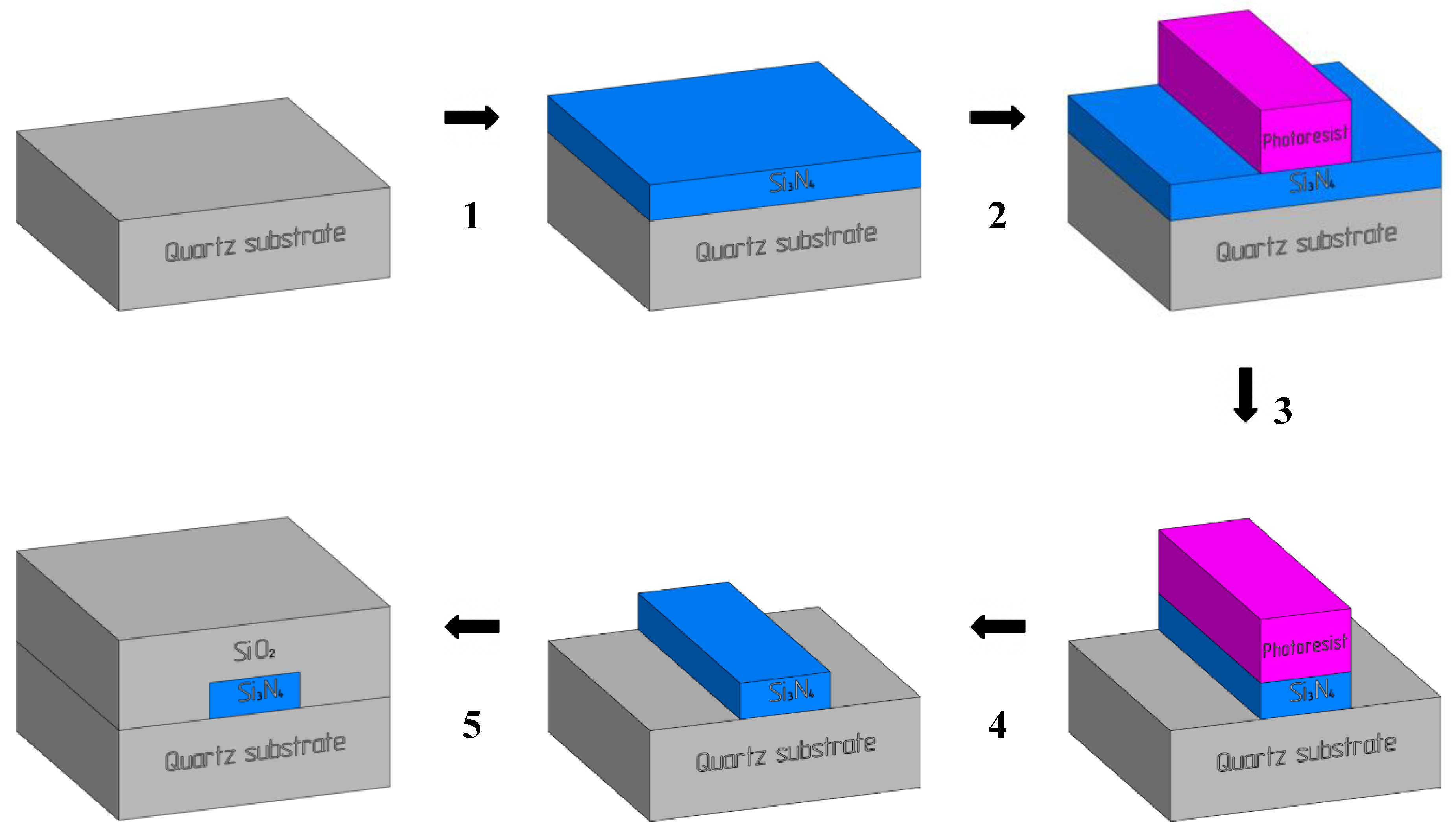
2. Fabrication
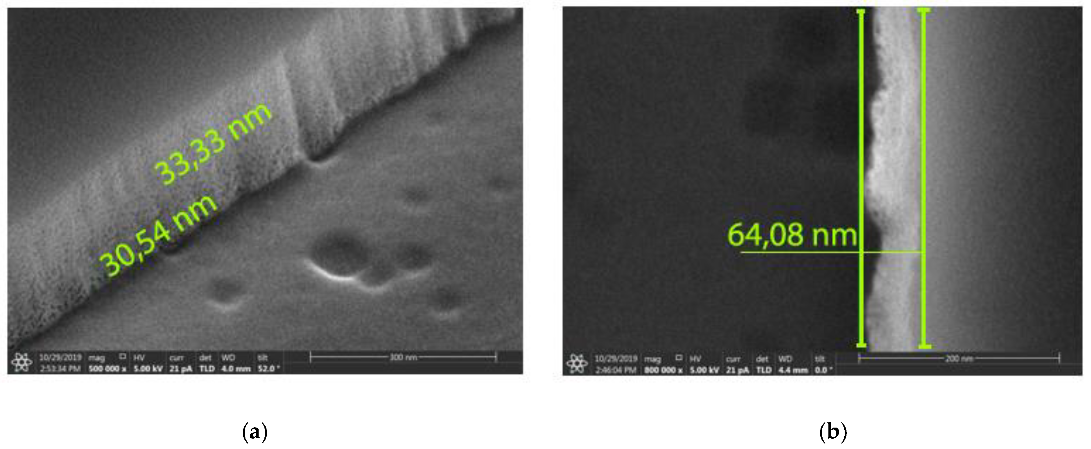
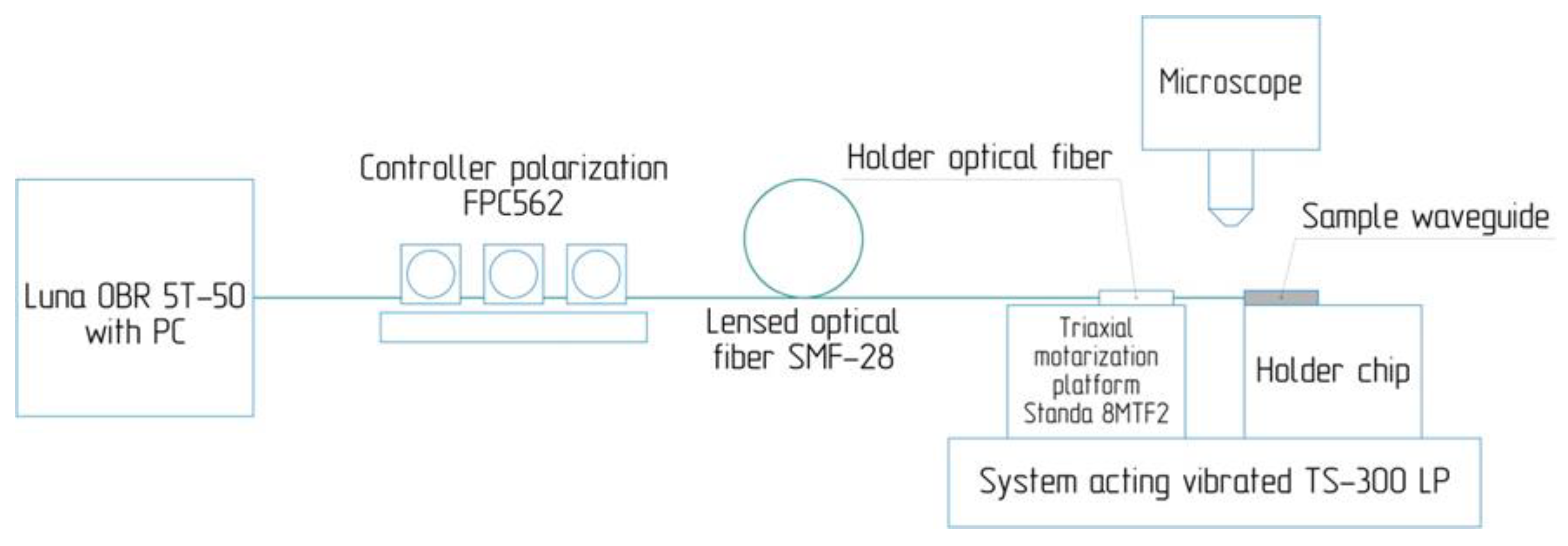
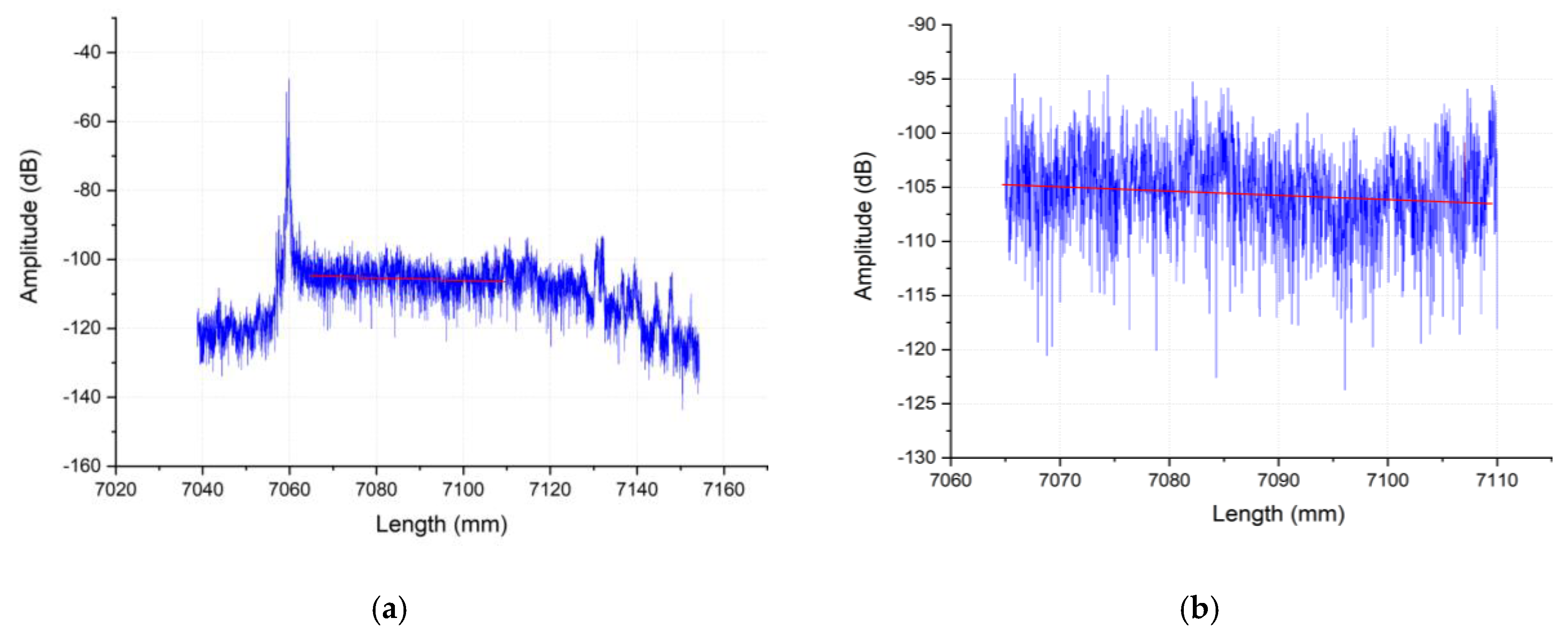
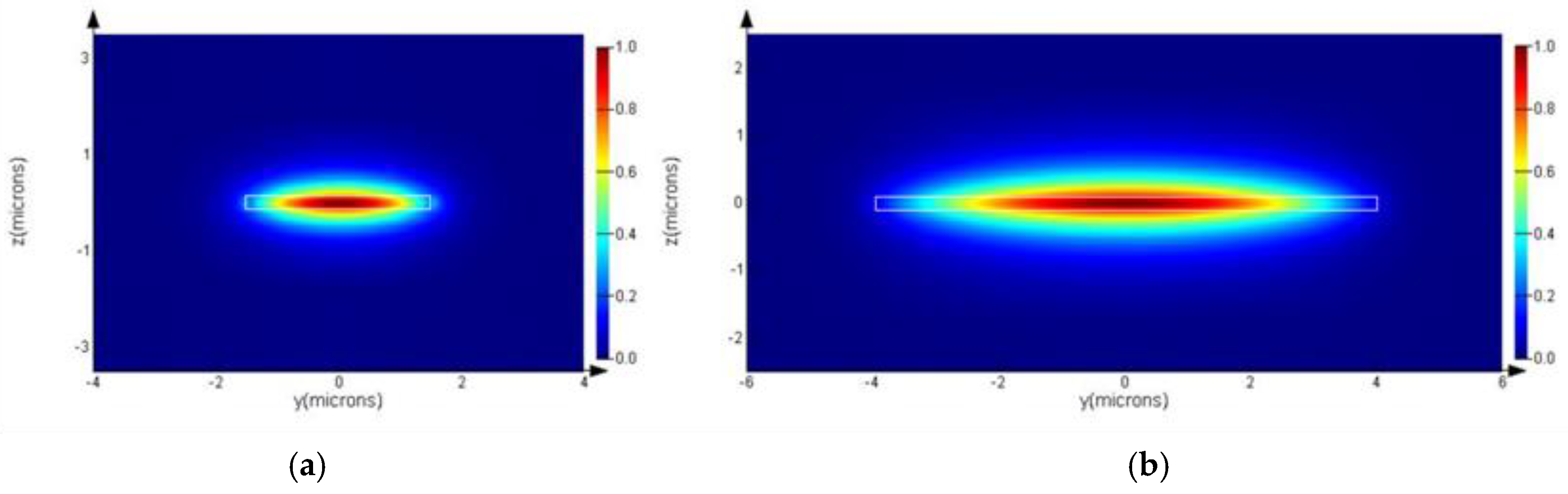
3. Study of Fabricated Waveguides
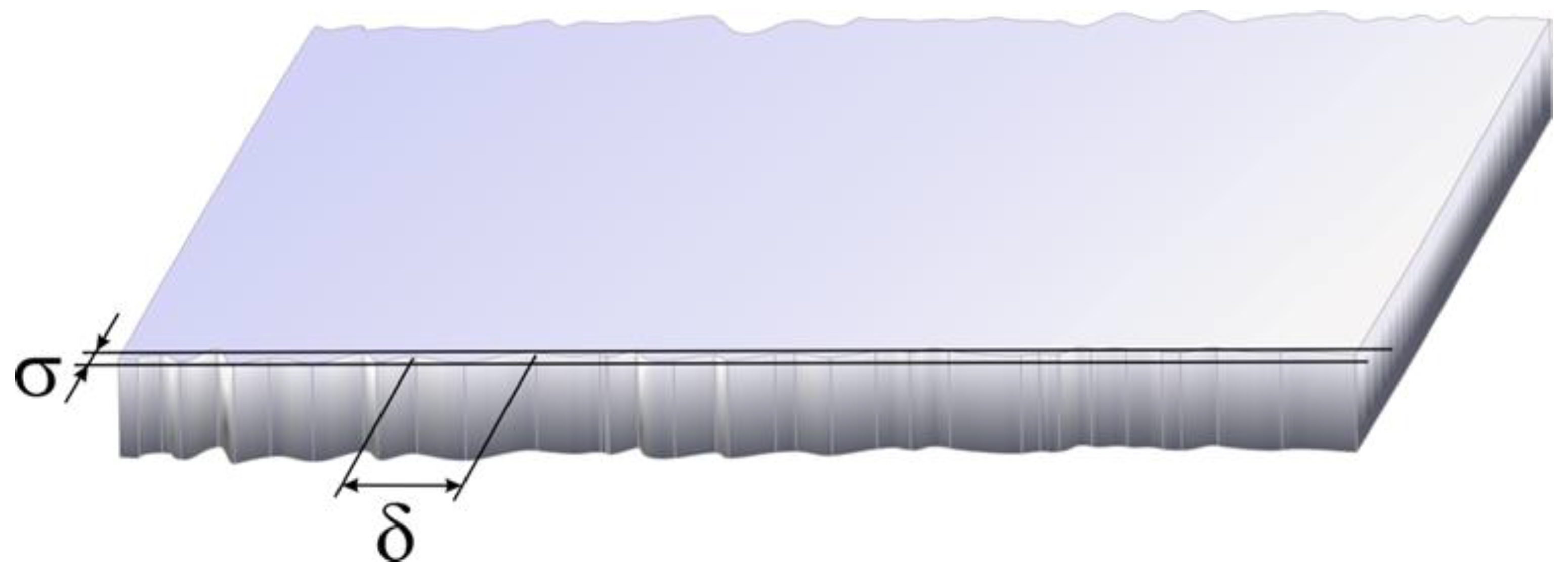
4. Calculation of the Influence of the Side Walls’ Roughness of a Silicon Nitride Layer on Optical Losses in the Waveguide
5. Conclusions
Author Contributions
Funding
Acknowledgments
Conflicts of Interest
References
- Doerr, C.R. Silicon photonic integration in telecommunications. Front. Phys. 2015, 3, 37. [Google Scholar] [CrossRef]
- Baets, R.G.F.; Subramanian, A.Z.; Clemmen, S.; Kuyken, B.; Bienstman, P.; Le Thomas, N.; Roelkens, G.; Van Thourhout, D.; Helin, P.; Severi, S. Silicon Photonics: Silicon nitride versus silicon-on-insulator. In Proceedings of the Optical Fiber Communication Conference, Anaheim, CA, USA, 20–22 March 2016; The Optical Society: Washington, DC, USA, 2016; p. Th3J.1. [Google Scholar]
- Li, C.; Liu, D.; Dai, D. Multimode silicon photonics. Nanophotonics 2018, 8, 227–247. [Google Scholar] [CrossRef]
- Streshinsky, M.; Ding, R.; Liu, Y.; Novack, A.; Galland, C.; Lim, A.E.-J.; Lo, P.G.-Q.; Baehr-Jones, T.; Hochberg, M. The Road to Affordable, Large-Scale Silicon Photonics. Opt. Photonics News 2013, 24, 32–39. [Google Scholar] [CrossRef]
- Dai, D. Advanced Passive Silicon Photonic Devices With Asymmetric Waveguide Structures. Proc. IEEE 2018, 106, 2117–2143. [Google Scholar] [CrossRef]
- Kribich, K.; Copperwhite, R.; Barry, H.; Kolodziejczyk, B.; Sabattié, J.-M.; O’Dwyer, K.; MacCraith, B. Novel chemical sensor/biosensor platform based on optical multimode interference (MMI) couplers. Sens. Actuators B Chem. 2005, 107, 188–192. [Google Scholar] [CrossRef]
- Pustelny, T.; Grabka, M. Numerical Investigation of the Photonic-Crystal Fibres with Suspended Core. Acta Phys. Pol. A 2009, 116, 385–388. [Google Scholar] [CrossRef]
- Mazingue, T.; Kribich, R.; Etienne, P.; Moreau, Y. Simulations of refractive index variation in a multimode interference coupler: Application to gas sensing. Opt. Commun. 2007, 278, 312–316. [Google Scholar] [CrossRef]
- Szewczuk, A.; Blahut, M. Multimode Interference Structures of Variable Geometry for Optical Sensor Application. Acta Phys. Pol. A 2010, 118, 1254–1258. [Google Scholar] [CrossRef]
- Masini, G.; Capellini, G.; Witzens, J.; Gunn, C. High-speed, monolithic CMOS receivers at 1550 nm with Ge on Si waveguide photodetectors. In Proceedings of the LEOS 2007-IEEE Lasers and Electro-Optics Society Annual Meeting Conference Proceedings, Lake Buena Vista, FL, USA, 21–25 October 2007; pp. 848–849. [Google Scholar]
- Feng, D.; Luff, B.J.; Asghari, M. Recent advances in manufactured silicon photonics integrated circuits. In Optoelectronic Integrated Circuits XIV; International Society for Optics and Photonics: Bellingham, WA, USA, 2012; Volume 8265, p. 826507. [Google Scholar]
- Pikhtin, N.A.; Slipchenko, S.O.; Sokolova, Z.N.; Tarasov, I.S. Internal optical loss in semiconductor lasers. Phys. Technol. Semicond. 2004, 38, 360–367. [Google Scholar] [CrossRef]
- Madani, A.; Kleinert, M.; Stolarek, D.; Zimmermann, L.; Ma, L.; Schmidt, O.G. Vertical optical ring resonators fully integrated with nanophotonic waveguides on silicon-on-insulator substrates. Opt. Lett. 2015, 40, 3826–3829. [Google Scholar] [CrossRef] [PubMed] [Green Version]
- Frankis, H.C.; Kiani, K.M.; Bonneville, D.B.; Zhang, C.; Norris, S.; Mateman, R.; Leinse, A.; Bassim, N.D.; Knights, A.P.; Bradley, J.D.B. Low-loss TeO2-coated Si3N4 waveguides for application in photonic integrated circuits. Opt. Express 2019, 27, 12529–12540. [Google Scholar] [CrossRef]
- Subramanian, A.Z.; Neutens, P.; Dhakal, A.; Jansen, R.; Claes, T.; Rottenberg, X.; Peyskens, F.; Selvaraja, S.; Helin, P.; Du Bois, B.; et al. Low-loss singlemode PECVD silicon nitride photonic wire waveguides for 532–900 nm wavelength window fabricated within a CMOS pilot line. IEEE Photonics J. 2013, 5, 2202809. [Google Scholar] [CrossRef] [Green Version]
- Huang, Y.; Song, J.; Luo, X.; Liow, T.-Y.; Lo, G.-Q. CMOS compatible monolithic multi-layer Si_3N_4-on-SOI platform for low-loss high performance silicon photonics dense integration. Opt. Express 2014, 22, 21859–21865. [Google Scholar] [CrossRef] [PubMed]
- Romero-García, S.; Merget, F.; Zhong, F.; Finkelstein, H.; Witzens, J. Silicon nitride CMOS-compatible platform for integrated photonics applications at visible wavelengths. Opt. Express 2013, 21, 14036–14046. [Google Scholar] [CrossRef]
- Cirino, G.A.; Barea, L.A.; Von Zuben, A.A.; L’Hermite, H.; Beche, B.; De Sagazan, O.; Frateschi, N.; Brahim, M.-T. Simulation and fabrication of silicon nitride microring resonator by DUV lithography. In Proceedings of the 2016 31st Symposium on Microelectronics Technology and Devices (SBMicro), Belo Horizonte, Brazil, 29 August–3 September 2016; IEEE: Piscataway, NJ, USA, 2016; pp. 1–4. [Google Scholar]
- Daldosso, N.; Melchiorri, M.; Riboli, F.; Girardini, M.; Pucker, G.; Crivellari, M.; Bellutti, P.; Lui, A.; Pavesi, L. Comparison among various Si/sub 3/N/sub 4/waveguide geometries grown within a CMOS fabrication pilot line. J. Lightwave Technol. 2004, 22, 1734–1740. [Google Scholar] [CrossRef]
- Gorin, A.; Jaouad, A.; Grondin, E.; Aimez, V.; Charette, P. Fabrication of silicon nitride waveguides for visible-light using PECVD: A study of the effect of plasma frequency on optical properties. Opt. Express 2008, 16, 13509–13516. [Google Scholar] [CrossRef] [Green Version]
- Gondarenko, A.; Levy, J.S.; Lipson, M. High confinement micron-scale silicon nitride high Q ring resonator. Opt. Express 2009, 17, 11366–11370. [Google Scholar] [CrossRef] [PubMed] [Green Version]
- Levy, J.S.; Gondarenko, A.; Foster, M.A.; Turner-Foster, A.C.; Gaeta, A.L.; Lipson, M. CMOS-compatible multiple-wavelength oscillator for on-chip optical interconnects. Nat. Photonics 2009, 4, 37–40. [Google Scholar] [CrossRef]
- Razzari, L.; Duchesne, D.; Ferrera, M.; Morandotti, R.; Chu, S.; Little, E.B.; Moss, D.J. CMOS-compatible integrated optical hyper-parametric oscillator. Nat. Photonics 2009, 4, 41–45. [Google Scholar] [CrossRef]
- Ferdous, F.; Miao, H.; Leaird, D.E.; Srinivasan, K.; Wang, J.; Chen, L.; Varghese, L.T.; Weiner, A.M. Spectral line-by-line pulse shaping of on-chip microresonator frequency combs. Nat. Photonics 2011, 5, 770–776. [Google Scholar] [CrossRef]
- Pfeifle, J.; Weimann, C.; Bach, F.; Riemensberger, J.; Hartinger, K.; Hillerkuss, D.; Jordan, M.; Holtzwarth, R.; Kippenberg, T.J.; Leuthold, J.; et al. Microresonator-Based Optical Frequency Combs for High-Bitrate WDM Data Transmission; The Optical Society of America: Washington, DC, USA, 2012; p. OW1C.4. [Google Scholar]
- Kippenberg, T.J.; Gaeta, A.L.; Lipson, M.; Gorodetsky, M.L. Dissipative Kerr solitons in optical microresonators. Science 2018, 361, eaan8083. [Google Scholar] [CrossRef] [PubMed] [Green Version]
- Halir, R.; Okawachi, Y.; Levy, J.S.; Foster, M.A.; Lipson, M.; Gaeta, A.L. Ultrabroadband supercontinuum generation in a CMOS-compatible platform. Opt. Lett. 2012, 37, 1685–1687. [Google Scholar] [CrossRef] [PubMed] [Green Version]
- Goykhman, I.; Desiatov, B.; Levy, U. Ultrathin silicon nitride microring resonator for biophotonic applications at 970 nm wavelength. Appl. Phys. Lett. 2010, 97, 81108. [Google Scholar] [CrossRef] [Green Version]
- Voirin, G.; Gehriger, D.; Parriaux, O.M.; Usievich, B.A. Si3N4/SiO2/Si waveguide grating for fluorescent biosensors. In Integrated Optics Devices III; International Society for Optics and Photonics: Bellingham, WA, USA, 1999; Volume 3620, pp. 109–116. [Google Scholar]
- Cai, H.; Poon, A.W. Optical trapping of microparticles using silicon nitride waveguide junctions and tapered-waveguide junctions on an optofluidic chip. Lab Chip 2012, 12, 3803–3809. [Google Scholar] [CrossRef] [PubMed]
- Tombez, L.; Zhang, E.J.; Orcutt, J.S.; Kamlapurkar, S.; Green, W.M.J. Methane absorption spectroscopy on a silicon photonic chip. Optica 2017, 4, 1322–1325. [Google Scholar] [CrossRef]
- Antonacci, G.; Goyvaerts, J.; Zhao, H.; Baumgartner, B.; Lendl, B.; Baets, R. Ultra-sensitive refractive index gas sensor with functionalized silicon nitride photonic circuits. arXiv 2020, arXiv:2004.04260. [Google Scholar] [CrossRef]
- Shaw, M.J.; Guo, J.; Vawter, G.A.; Habermehl, S.; Sullivan, C.T. Fabrication techniques for low-loss silicon nitride waveguides. In Micromachining Technology for Micro-Optics and Nano-Optics III; SPIE: Bellingham, WA, USA, 2005; Volume 5720, pp. 109–118. [Google Scholar]
- Moreira, R.L. Integrated Optical Delay Line Circuits on a Ultra-Low Loss Planar Waveguide Platform. Ph.D. Thesis, University of California, Santa Barbara, CA, USA, 2016. [Google Scholar]
- Shang, H.; Sun, D.; Yu, P.; Wang, B.; Yu, T.; Li, T.; Jiang, H. Investigation for Sidewall Roughness Caused Optical Scattering Loss of Silicon-on-Insulator Waveguides with Confocal Laser Scanning Microscopy. Coatings 2020, 10, 236. [Google Scholar] [CrossRef] [Green Version]
- Witzens, J.; Hochberg, M. Optical detection of target molecule induced aggregation of nanoparticles by means of high-Q resonators. Opt. Express 2011, 19, 7034–7061. [Google Scholar] [CrossRef]
- Neutens, P.; Subramanian, A.; Hasan, M.U.; Chen, C.; Jansen, R.; Claes, T.; Rottenberg, X.; Du Bois, B.; Leyssens, K.; Helin, P.; et al. Characterization of PECVD silicon nitride photonic components at 532 and 900 nm wavelength. Photonics Eur. 2014, 9133, 91331F. [Google Scholar]
- Bagatur’yants, A.A.; Minushev, A.K.; Novoselov, K.P.; Safonov, A.A.; Umanskii, S.Y.; Vladimirov, A.S.; Korkin, A. Atomistic Simulation of Si3N4 CVD from Dichlorosilane and NH3. In Predictive Simulation of Semiconductor Processing; Springer: Berlin/Heidelberg, Germany, 2004; pp. 295–355. [Google Scholar]
- LIGENTEC SA. Silicon Nitride LIGENTEC. Available online: https://www.ligentec.com/technology-ligentec/siliconnitride-ligentec/ (accessed on 3 April 2019).
- Bylina, M.S.; Glagolev, S.F.; Kochanovsky, L.N.; Piskunov, V.V. Measurement of Parameters of Fiber-Optic Linear Paths; Textbook; Department of Communication Lines SPb GUT by Prof. M.A. Bonch-Bruevich: St. Petersburg, Russian Federation, 2002. [Google Scholar]
- Soller, B.J.; Gifford, D.K.; Wolfe, M.S.; Froggatt, M.E. High resolution optical frequency domain reflectometry for characterization of components and assemblies. Opt. Express 2005, 13, 666–674. [Google Scholar] [CrossRef] [Green Version]
- Luke, K.; Okawachi, Y.; Lamont, M.R.E.; Gaeta, A.L.; Lipson, M. Broadband mid-infrared frequency comb generation in a Si3N4 microresonator. Opt. Lett. 2015, 40, 4823–4826. [Google Scholar] [CrossRef]
- Lin, P.T.; Singh, V.; Lin, H.-Y.G.; Tiwald, T.; Kimerling, L.C.; Agarwal, A.M. Low-Stress Silicon Nitride Platform for Mid-Infrared Broadband and Monolithically Integrated Microphotonics. Adv. Opt. Mater. 2013, 1, 732–739. [Google Scholar] [CrossRef]
- Shao, Z.; Chen, Y.; Chen, H.; Zhang, Y.; Zhang, F.; Jian, J.; Fan, Z.; Liu, L.; Yang, C.; Zhou, L.; et al. Ultra-low temperature silicon nitride photonic integration platform. Opt. Express 2016, 24, 1865–1872. [Google Scholar] [CrossRef]


| Silicon | Silicon Nitride | Silicon Oxide | |
|---|---|---|---|
| Transparency | 1.1–9 µm | 0.25–8 µm | 0.13–3.5 µm |
| Band gap | 1.12 eV | 5 eV | 9 eV |
| Refractive index at 1550 nm | 3.8 | 2.00 | 1.46 |
| Nonlinear coefficient (m2W−1) | ≈6 × 10⁻¹⁸ | ≈2 × 10⁻¹⁹ | ≈2.5 ×10⁻²⁰ |
| Deposition | Crystal EPI/SOI | LPCVD | Thermal oxide |
| Waveguide Structure Width, µm | Optical Loss, dB/cm |
|---|---|
| 3 | 1.43 |
| 8 | 0.31 |
| Waveguide Structure Width, µm | Optical Loss (Measured), dB/cm | σ, nm | δ, nm | Optical Loss (Calculated), dB/cm |
|---|---|---|---|---|
| 3.00 | 1.43 | 30.00 | 20.00 | 1.63 |
| 30.00 | 60.00 | 1.27 | ||
| 10.00 | 20.00 | 0.22 | ||
| 8.00 | 0.31 | 30.00 | 20.00 | 0.11 |
| 30.00 | 60.00 | 0.05 | ||
| 10.00 | 20.00 | 0.01 |
Publisher’s Note: MDPI stays neutral with regard to jurisdictional claims in published maps and institutional affiliations. |
© 2020 by the authors. Licensee MDPI, Basel, Switzerland. This article is an open access article distributed under the terms and conditions of the Creative Commons Attribution (CC BY) license (http://creativecommons.org/licenses/by/4.0/).
Share and Cite
Yakuhina, A.; Kadochkin, A.; Svetukhin, V.; Gorelov, D.; Generalov, S.; Amelichev, V. Investigation of Side Wall Roughness Effect on Optical Losses in a Multimode Si3N4 Waveguide Formed on a Quartz Substrate. Photonics 2020, 7, 104. https://0-doi-org.brum.beds.ac.uk/10.3390/photonics7040104
Yakuhina A, Kadochkin A, Svetukhin V, Gorelov D, Generalov S, Amelichev V. Investigation of Side Wall Roughness Effect on Optical Losses in a Multimode Si3N4 Waveguide Formed on a Quartz Substrate. Photonics. 2020; 7(4):104. https://0-doi-org.brum.beds.ac.uk/10.3390/photonics7040104
Chicago/Turabian StyleYakuhina, Anastasia, Alexey Kadochkin, Vyacheslav Svetukhin, Dmitry Gorelov, Sergey Generalov, and Vladimir Amelichev. 2020. "Investigation of Side Wall Roughness Effect on Optical Losses in a Multimode Si3N4 Waveguide Formed on a Quartz Substrate" Photonics 7, no. 4: 104. https://0-doi-org.brum.beds.ac.uk/10.3390/photonics7040104