A Closer Look at Photonic Nanojets in Reflection Mode: Control of Standing Wave Modulation


1
Institute of Automation and Control Processes FEB RAS, 5 Radio Str., 690041 Vladivostok, Russia
2
Nondestructive School of Tomsk Polytechnic University, 30 Lenin Ave., 634050 Tomsk, Russia
*
Author to whom correspondence should be addressed.
Photonics 2021, 8(2), 54; https://0-doi-org.brum.beds.ac.uk/10.3390/photonics8020054
Submission received: 27 December 2020
/
Revised: 8 January 2021
/
Accepted: 15 February 2021
/
Published: 17 February 2021
(This article belongs to the Special Issue Photonic Jet: Science and Application)
Abstract
:The photonic nanojet phenomenon is commonly used both to increase the resolution of optical microscopes and to trap nanoparticles. However, such photonic nanojets are not applicable to an entire class of objects. Here we present a new type of photonic nanojet in reflection mode with the possibility to control the modulation of the photonic nanojet by a standing wave. In contrast to the known kinds of reflective photonic nanojets, the reported one occurs when the aluminum oxide hemisphere is located at a certain distance from the substrate. Under illumination, the hemisphere generates a primary photonic nanojet directed to the substrate. After reflection, the primary nanojet acts as an illumination source for the hemisphere, leading to the formation of a new reflective photonic nanojet. We show that the distance between the hemisphere and substrate affects the phase of both incident and reflected radiation, and due to constructive interference, the modulation of the reflective photonic nanojet by a standing wave can be significantly reduced. The results obtained contribute to the understanding of the processes of photonic nanojet formation in reflection mode and open new pathways for designing functional optical devices.
1. Introduction
Along with plasmonics, dielectric photonics [1] is associated with the processes of localization of light and is aimed at increasing the efficiency of the interaction of incident radiation with matter. The progress in this direction contributes to the development of compact optical radiation control devices, opening opportunities for the creation of new sensing structures [2], detection of nano- and microparticles [3,4,5,6], nanoparticle manipulation [7,8], luminescence [9,10] and Raman scattering enhancement [11], and both optical [12,13] and terahertz [14] super-resolution microscopy. Moreover, dielectric photonic structures are free from the disadvantages associated with extremely high losses that occur with plasmonic structures, which significantly increases the efficiency of devices based on them [15].
Localization of light requires sharp focusing, which can be achieved by high-numerical-aperture diffractive optical elements [16]. To date, the most popular approach for micro- and nanoobject manipulation is the use of various metalenses. In general, a metalens consists of many distributed microstructures that adjust the incident light to be focused from several tens of micrometers [17,18] to several millimeters [19]. For example, some authors [20] used a reflective metalens with a size of 100 μm × 100 μm, which corresponds to lens dimensions of 93.98λ × 93.98λ at λ = 1064 nm with a focal length of 108λ, almost equal to the lens diameter. Moreover, the beam waist radius was equal to 0.62λ, i.e., greater than the diffraction limit. These are the typical size and parameters of microlenses [16].
Although the light cannot be directly focused into the subwave region, for certain sizes of the dielectric microparticle, it can be “limited” in all three dimensions due to the specific interference of the radiation transmitted and scattered on the microstructure—an effect called a “photonic nanojet” (PNJ) [13,21]. In the photonic nanojet phenomenon, the scattering is characterized by the refractive index n as well as the Mie size parameter , if the dielectric particle has no dissipation. Usually, to form a PNJ, the size parameter is q = (10…20)π [22,23] and takes an intermediate value between the dipole approximation for smaller particles (R ≪ λ) and the geometrical optics approximation for the largest particles (including lenses, q > 100π). In contrast to metalenses, the use of a photonic nanojet allows for localizing the incident radiation into the subwavelength region using a mesoscale particle-lens near its surface, with a characteristic size on the order of or slightly larger than the wavelength with beam waist radius less than the diffraction limit [21,22,23]. Accordingly, the size of the focusing structure can be reduced by about 100 times, compared to classical high-numerical-aperture lenses with increasing focused field localization below the diffraction limit. The size of a single phase-tuning element in metalenses has a wavelength scale, which is comparable with the size of a PNJ-generating microstructure [21]. In this regard, the same technique used for metalens fabrication could be used for the creation of arrays of PNJ-generated microstructures, opening a way for the development of new functional structures.
Subwavelength light localization via photonic nanojets not only simplifies the trapping of nano- and micro-objects but also allows us to reduce the intensity of “trapping light”. In [24], a PNJ with localization intensity (ratio of the intensities of the focal spot and incident light) equal to 4 was used to trap 50-nm-sized gold nanoparticles and track the trapping event through backscattered light. The minimal PNJ intensity for nanoparticle trapping seems to be around 3 [7], allowing operation with sub-100-nm-sized particles. Enhancement of the photoluminescence (PL) or Raman scattering signal is the other promising field for PNJ application. A tenfold enhancement of ZnO thin-film PL was achieved using a PNJ generated by 5-μm-sized fused silica and polystyrene microspheres [25]. This PL enhancement arises from modifications of the optical density of states in ZnO due to the Purcell effect [26] with a threshold starting from a PNJ intensity of 3.5. In turn, the lowest PNJ intensity for Raman scattering enhancement was reported to be 2.3 [27].
Most studies of photonic nanojets have aimed at obtaining sharp-focused high-intensity regions of radiation localization in transmission mode, so such functional structures are not suitable for “traditional” optical and fluorescent microscopes operated in reflection geometry. In this regard, the development of new functional structures generating PNJs in reflection mode allows us to combine the unique properties of PNJs and simplify techniques for their implementation. In general, the formation of a reflective photonic nanojet from a dielectric microparticle occurs due to the interaction of reflected light, passed through the parental microparticle, with the incident light, leading to modulation of the photonic nanojet by a standing wave [28,29,30,31]. This feature has great practical importance since it allows for achieving a relatively high localization intensity in the simplest experimental geometry. The process of PNJ formation in this geometry is well-studied theoretically [28,29,30,31,32], and one can find methods for its implementation in real experiments. For example, the stability of the Brownian motion of nanoparticles could be improved by using a reflective photonic nanojet [16,30]. It is also well known that optical devices, like a microscope, or surface-enhanced Raman scattering and photoluminescence-enhancing structures, can operate in both transmission and reflection modes [33,34,35].
Here we show that it is possible to avoid modulation of the photonic nanojet by a standing wave by placing, for example, an aluminum oxide hemisphere [36] at a certain distance (a gap) from a silicon substrate and using a low-coherence excitation source. The results obtained indicate that the generated PNJ shows behavior similar to that of a “classical” PNJ in reflection mode, so it is possible to distinguish the processes involved in its formation. To provide a link between numerical and experimental studies of the formation of this kind of PNJ, we fabricated an ordered array of aluminum oxide microspheres with numerically predicted optical and size parameters and performed direct experimental measurements of the reflective photonic nanojets generated. This, in turn, opens the way for microminiaturization of photonics for various purposes and applications.
2. Materials and Methods
The numerical simulations were performed via finite-difference time-domain modeling [37], performed in Matlab software. The simulation domain was a triangular mesh with a perfectly matched layer as a boundary. The mesh size was set equal to λ/25, where λ = 532 nm is an illuminating wavelength, to assure balance between accuracy and calculated speed. Space and time derivatives were both calculated via second-order accurate centered difference. The time step was determined by the size of the triangular mesh and selected to ensure numerical stability. A plane wave TE-polarized light with unit intensity was generated on the left side of the simulation domain. Calculations were conducted for two positions of a plane wave source with unit intensity: (i) at 3 μm above the hemisphere, which was a compromise between model accuracy and calculation time, and (ii) at 100 nm above the parental microstructure to exclude parasitic interference between the light source and the PNJ generated in reflection mode. To provide a link with further practical applications of the PNJ studied, the refractive index of the propagating media was chosen to be nc = 1.545, which is common for various polymeric materials [38]. The refractive indices of polymethylmethacrylate (PMMA), alumina, and silicon are 1.495, 1.7731, and 4.22469, respectively, at the incident wavelength [39,40].
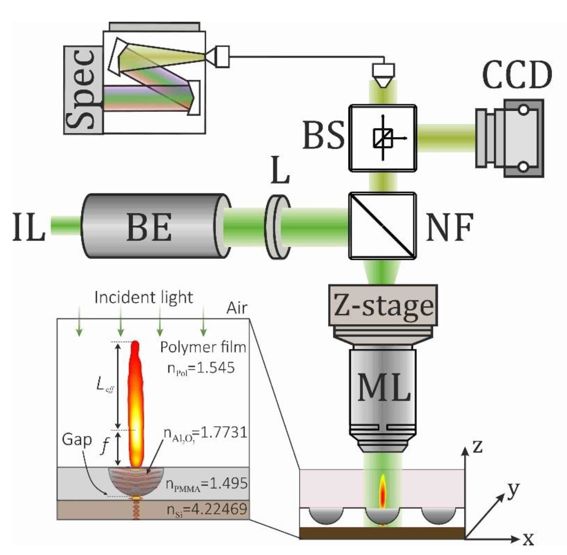
Direct experimental studies of the photonic nanojet formation were carried out via a specially built setup (Figure 1). This setup allows one to simultaneously record the luminescent signal from an area on the order of three square micrometers. A charge-coupled device (CCD) array and an Andor high-speed spectrometer were used for image capture and spectral measurements, correspondingly. The size of the CCD was 35.9 × 24 mm with a pixel size of 5.9 μm, and the resolution was 6016 × 4016 pixels. The Andor spectrometer was equipped with a Shamrock 750 monochromator and an iStar camera. The monochromator had three motorized diffraction gratings with 600, 1200, and 2400 lines per millimeter, and the maximum spectral resolution was 0.3 nm. The iStar camera is a cooled CCD with a pixel size of 13 × 13 microns, providing a maximum shooting speed of 1.3 ns. A Nikon λ Plan Apo series microscope lens (NA0.9, 100x) was used to construct images. The lens was mounted on a piezoelectric positioner (movement range along the Z-axis, 400 μm; accuracy, 10 nm; minimal step, 4 nm). An adjustable neutral optical density filter (variable optical density from 0.1 to 4) was used to balance the incident radiation intensity for the constructed image and spectral intensity measurements. During image construction, the objective formed a slightly divergent light beam, which was then divided into two channels. The first beam was directed to the CCD that captured the image, and the second one was collected by the fiber input of the spectrometer (core diameter, 300 μm), acting as a pinhole in the confocal scheme. The CCD and the fiber input of the spectrometer were placed at the same distance from the beam-splitting cube; hence, the images of the working area captured by CCD and the one directed to the spectrometer had the same lateral dimensions.
The NKT Photonics SuperK Extreme broadband coherent light source was used as an incident light source; it generates radiation in the range of 450–1800 nm and was equipped with an acousto-optic filter unit with the possibility to select the required wavelength with a spectral half-width of 5 nm and average power of 3 mW. This source has low spatial coherence and emits an almost unpolarized light, which allows one to reduce as much as possible the occurrence of interference events during measurements.
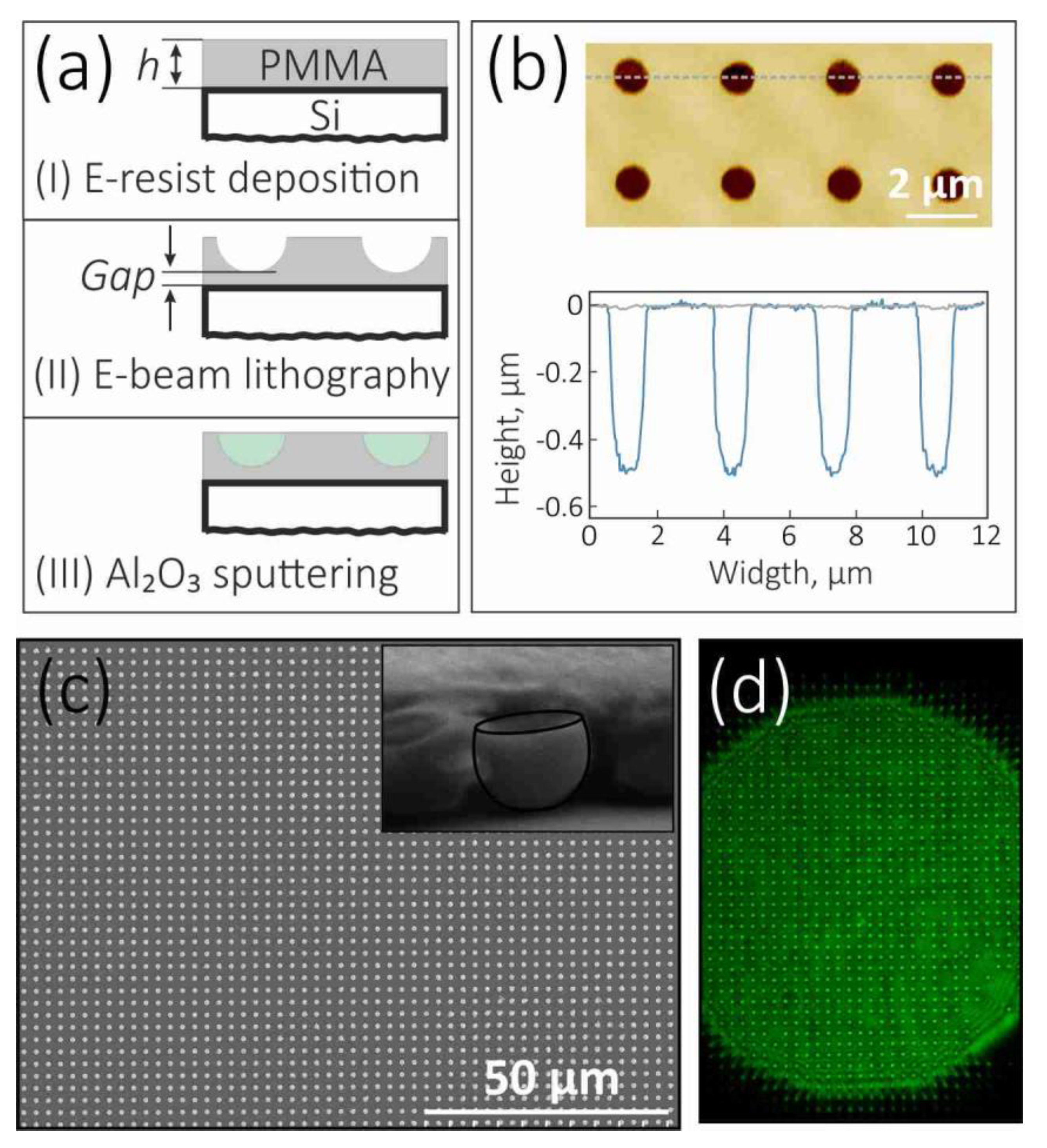
The fabrication of dielectric structures with precalculated geometric parameters was carried out by a combination of methods of electron beam lithography, vacuum deposition, and selective chemical etching. These methods are the standard technological approaches used in silicon microelectronics and, thus, could be used in further serial production of functional optical devices based on PNJ phenomena. A schematic representation of the dielectric microstructure fabrication process is shown in Figure 2a and, in general, consisted of three steps. In the first step, a PMMA layer was spin-coated onto a silicon substrate. To provide higher mechanical stability of the PMMA film and avoid probable damage during further development, the film was annealed at 150 °C for 3 h, resulting in total removal of the remaining solvent molecules and reduction of the internal stresses in the film due to its transformation from liquid to solid state. After that, the pattern for the future microparticle array with the required hemispherical profile was formed in the PMMA film via electron beam lithography. The exposure dose and scanning rate were adjusted in such a way as to ensure a hemispherical profile to be written in the volume of PMMA film, keeping the required gap distance between the microstructures and substrate. It is well known that PMMA is a positive resist, and its molecules break during exposure to an electron beam. As a result, the exposed areas become soluble in the developer solution (9:1 mixture of isopropyl alcohol with water). The resulting array of holes in the PMMA film acted as a template for microparticle creation via the vacuum deposition technique. The quality of the template, e.g., the depth of the microholes and its surface profile, was controlled via the atomic-force microscopy (AFM) technique (Figure 2b), which revealed that the average upper diameter of microholes was about 1000 ± 40 nm, with 500 ± 10 nm depth. The alumina deposition was performed using a PVD-2EB2R11 vacuum deposition device (ADVAVAC, Canada) equipped with a magnetron sputtering system, allowing deposited layer thickness control of up to 1 nm. To increase adhesion, before deposition, the sample was activated by argon plasma.
In general, the fabricated arrays occupy an area of 400 × 400 μm. In the case of a 1-μm-diameter aluminum oxide hemisphere, the array contains 17.5 thousand single microstructures. Figure 2c shows a scanning electron microscope (SEM) image of a 135 × 100 μm area with more than 2000 uniformly distributed dielectric microstructures of the same lateral size. In turn, a 0.9NA-100× microscope lens, used in our setup for image construction, provided simultaneous capture of the PNJs from approximately 1000 microstructures (Figure 2d), giving plenty of room for precise high-resolution optical measurements. It should be noted that microstructures could be resolved using even a 0.6NA microscope lens with 40× or 60× magnification. However, a low-resolution lens does not allow direct measurements of a single PNJ’s intensity, because there are about 20 microstructures in a field of view of the fiber-optical signal collection system.
3. Results and Discussion
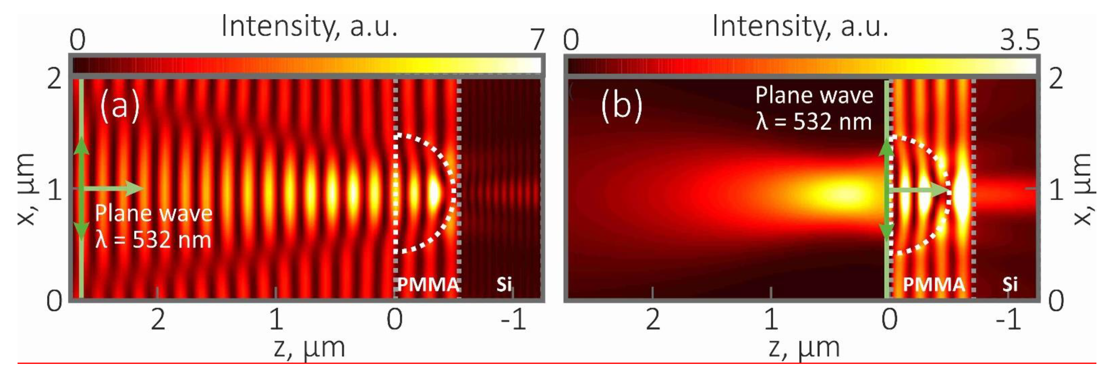
The numerically simulated pattern of the reflective photonic nanojet’s modulation by a standing wave is shown in Figure 3a. It was found that the use of a low-coherence light source made it possible to reduce the interference between the incident and reflected light, resulting in “uniform” PNJ formation, without the appearance of the interference pattern (Figure 3b).
It is interesting to note that both types of PNJs (generated by or without interference with incident light) have pretty similar properties: (i) the maximum localization intensity is separated from the hemisphere’s surface and located at ≈0.8λ from it; (ii) the PNJ length (Leff), defined as the distance where the maximal PNJ intensity (Imax) decreases by e times, is also almost the same and equal to 1.7 μm or ≈3λ (in a case of an “interference-based” PNJ, this distance was estimated for interference maxima); (iii) the FWHM of PNJs in a maximum-intensity area is also similar and equal to 0.75 λ. The quality factor (Q) was determined as [22,41]
where FWHM is the full width at half-maximum of the PNJ intensity; for PNJs generated without modulation by a standing wave, this is equal to 7.37 and close to the square root of Q for a PNJ with modulation (46.19), which also indicates the connection between these two PNJ types.
Taking into account the value of the quality factor and light intensity in the localization area, we believe that the new type of reflective photonic nanojet described above may replace different types of objective lenses (metalens) or arrays of lenses [42,43] in different miniaturized environments, including lab-on-a-chip devices, and could be suitable for the manipulation of nanoparticles and the enhancement of PL and Raman scattering signals as well. However, the use of such devices and applications is a challenge for future research.
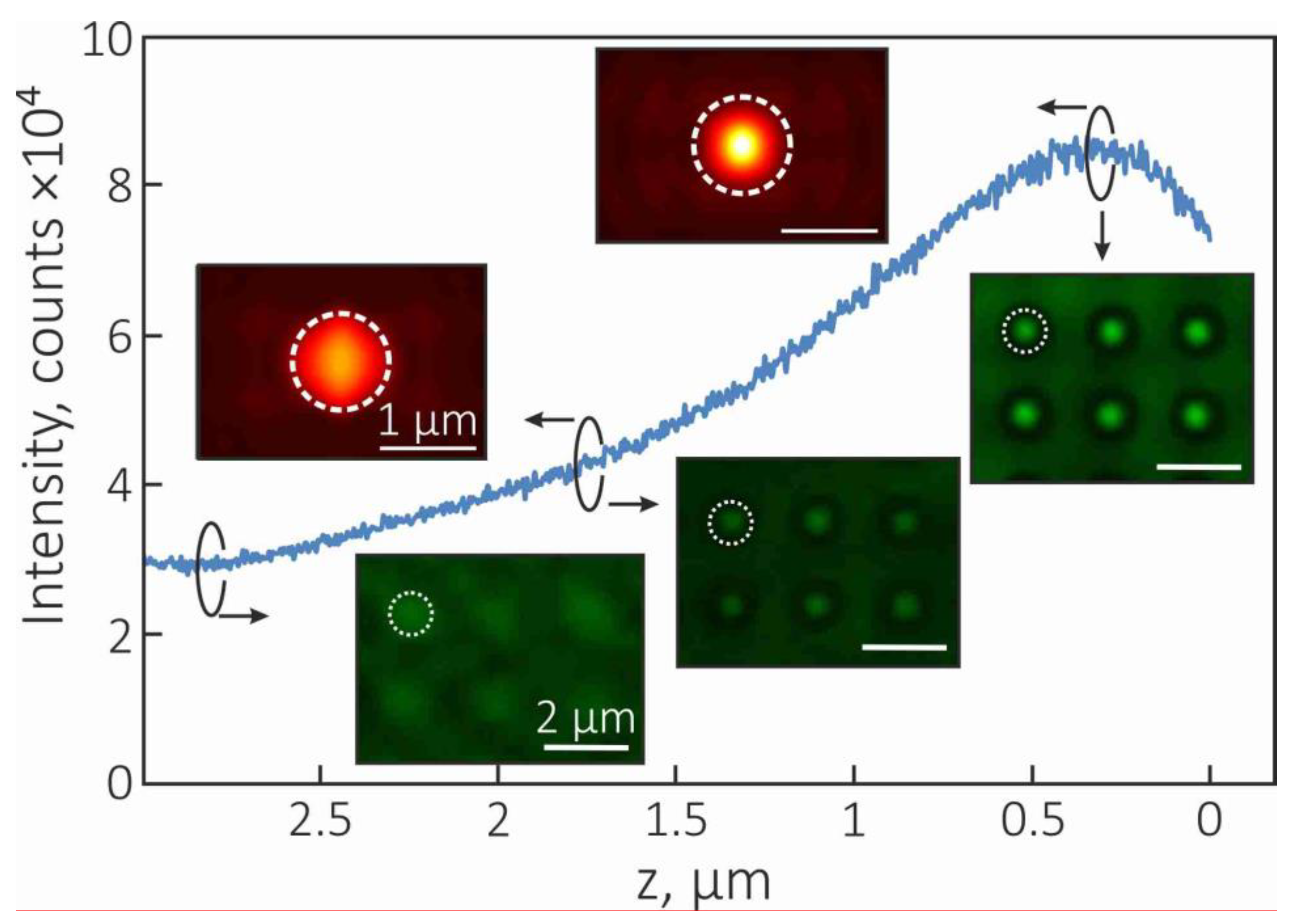
To provide experimental verification, we obtained the PNJ intensity distribution across its propagation length using the synchronizing spectrometer with the piezoelectric positioner to collect the intensity at every movement step (≈4 nm). The experimentally measured PNJ intensity distribution was in good agreement with the numerically calculated one (Figure 4). Moreover, the PNJ images captured at the maximum-intensity point (0.4 μm on the Z-axis), on the end of an effective PNJ length (1.5 μm on the Z-axis), and at the very end of the PNJ, where its intensity becomes close to the background level (2.8 μm on the Z-axis), were also in a good agreement with the calculated ones. The results obtained prove the possibility of PNJ generation in reflection mode without modulation by a standing wave.
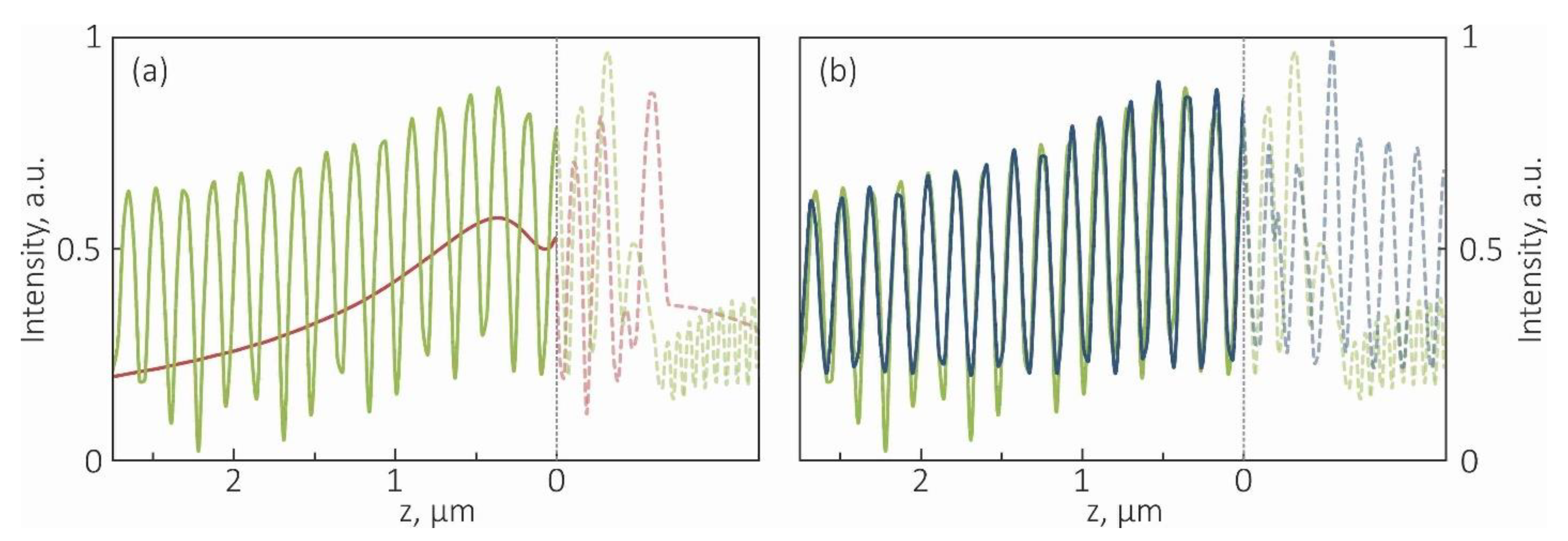
The next question to be solved is to distinguish the process of PNJ formation in reflection mode due to interference between reflected and incident light. The intensity distributions for both PNJ types (Figure 5a) illustrate the similar behavior of the PNJs, mentioned above in the Introduction section. This allows one to conclude that the interaction of a bare reflected PNJ with incident light can be described by the well-known interference equation [44] as follows:
where IPNJ is the intensity of the PNJ due to reflection from the substrate, and I0 is the incident light intensity; k = (nhs∙Rhs + Iφ)∙LZ is the reflected light phase shift caused by its passing through the gap (Iφ) and the hemisphere with refractive index nhs and radius Rhs, as well, during its backward propagation along the Z-axis over the distance LZ. It should be noted that inside the gap the additional interference pattern occurs, which could either enhance or quench the light reflected from the substrate.This feature is likely a reason for the nonmonotonic change in PNJ intensity with increasing the gap [36].
As a result, the “simulated” interference patterns [45] are quite well matched with the numerically calculated intensity distribution for PNJs formed due to interference between reflected and incident light (Figure 5b). Some mismatch in the modulation depth at distances above the effective PNJ length, and a significant mismatch in interference patterns in the gap and substrate area, may indicate the presence of additional factors affecting PNJ formation in reflection mode.
Analysis of the data presented in Figure 3, Figure 4 and Figure 5 allows us to assume the following mechanism of PNJ formation due to only light reflected from the substrate for the case when there is a certain gap between the parental microstructure and the substrate. After illumination, the hemisphere forms a primary PNJ on its shadow surface (this is a “classical” PNJ in transmission mode) [46]. This primary PNJ is located slightly apart (≈100 nm or ½ gap) from the hemisphere’s surface. When the primary PNJ is reflected back from the substrate, it acts as a new (effective) illumination source for the hemisphere, leading to the formation of a secondary PNJ, which appears to be the one PNJ formed due to bare reflection from a substrate. In fact, by choosing the value of the gap, we controlled the phases of radiation both incident and reflected from the substrate, and due to constructive interference, the modulation of the reflective photonic nanojet by a standing wave was significantly reduced. From this point of view, concerning the new excitation source position, the secondary PNJ is formed as in transmission mode and, thus, could exist without modulation by the standing wave.
4. Conclusions
A new type of photonic nanojet in reflection mode without modulation by a standing wave was numerically and experimentally predicted herein. This nanojet was generated by an aluminum oxide micro-hemisphere placed at a certain gap from the silicon substrate and occurred under low-coherence light illumination. In this case, the parental microstructure first generated a PNJ in transmission mode that, after reflection from the substrate, acted as a new effective excitation source for the microstructure. The exact gap value depended on the parental microstructure parameters: size, shape, refractive index contrast with surrounding media, and substrate parameters (i.e., reflection coefficient, refractive index, etc. [21,28,47]) that determine the properties of light reflection from the substrate, thus affecting the final PNJ properties. Taking into account that the PNJ properties depend on refractive index contrast [21,27,39,48], it is possible to adjust these properties by changing the material of the microstructure, its surrounding media, substrate parameters, and/or the gap value. The results obtained are promising for optical sensing, surface-enhanced Raman scattering [11,27], optical data processing, nanoparticle manipulations, sorting and imaging of micro- and nanoobjects, and studies in reflection geometry using a regular confocal microscope [49].
Author Contributions
Conceptualization, I.V.M. and O.V.M.; investigation K.A.S. and A.A.S.; writing—original draft preparation, K.A.S. and A.A.S.; writing—review and editing, I.V.M. and O.V.M. All authors have read and agreed to the published version of the manuscript.
Funding
The experimental studies of photonic nanojet formation in reflection mode were supported by the Russian Science Foundation (project 20-72-00066).
Data Availability Statement
Experimental data is available from the corresponding author upon reasonable request.
Acknowledgments
I.V.M. and O.V.M. acknowledge the Tomsk Polytechnic University Competitiveness Enhancement Program.
Conflicts of Interest
The authors declare no conflict of interest.
References
- Baranov, D.; Zuev, D.; Lepeshov, S.; Kotov, O.; Krasnok, A.; Evlyukhin, A.; Chichkov, B. All-dielectric nanophotonics: The quest for better materials and fabrication techniques. Optica 2017, 4, 814–825. [Google Scholar] [CrossRef]
- Sergeeva, K.A.; Tutov, M.V.; Voznesenskiy, S.S.; Shamich, N.I.; Mironenko, A.Y.; Sergeev, A.A. Highly-sensitive fluorescent detection of chemical compounds via photonic nanojet excitation. Sens. Act. B 2020, 305, 127354. [Google Scholar] [CrossRef]
- Li, Y.; Xin, H.; Liu, X.; Zhang, Y.; Lei, H.; Li, B. Trapping and detection of nanoparticles and cells using a parallel photonic nanojet array. ACS Nano 2016, 10, 5800–5808. [Google Scholar] [CrossRef]
- Ren, Y.X.; Zeng, X.; Zhou, L.M.; Kong, C.; Mao, H.; Qiu, C.W.; Tsia, K.K.; Wong, K.K. Photonic nanojet mediated backaction of dielectric microparticles. ACS Photonics 2020, 7, 1483–1490. [Google Scholar] [CrossRef]
- Tomitaka, A.; Arami, H.; Ahmadivand, A.; Pala, N.; McGoron, A.J.; Takemura, Y.; Febo, M.; Nair, M. Magneto-plasmonic nanostars for image-guided and NIR-triggered drug delivery. Sci. Rep. 2020, 10, 1–10. [Google Scholar] [CrossRef] [PubMed]
- Yu, X.; Li, A.; Zhao, C.; Yang, K.; Chen, X.; Li, W. Ultrasmall semimetal nanoparticles of bismuth for dual-modal computed tomography/photoacoustic imaging and synergistic thermoradiotherapy. ACS Nano 2017, 11, 3990–4001. [Google Scholar] [CrossRef]
- Li, Y.C.; Xin, H.B.; Lei, H.X.; Liu, L.L.; Li, Y.Z.; Zhang, Y.; Li, B.J. Manipulation and detection of single nanoparticles and biomolecules by a photonic nanojet. Light Sci. Appl. 2016, 5, e16176. [Google Scholar] [CrossRef]
- Minin, I.V.; Minin, O.V.; Cao, Y.; Liu, Z.; Geints, Y.E.; Karabchevsky, A. Optical vacuum cleaner by optomechanical manipulation of nanoparticles using nanostructured mesoscale dielectric cuboid. Sci. Rep. 2019, 9, 12748. [Google Scholar] [CrossRef] [PubMed] [Green Version]
- Zhang, W.; Lei, H. Fluorescence enhancement based on cooperative effects of a photonic nanojet and plasmon resonance. Nanoscale 2020, 12, 6596–6602. [Google Scholar] [CrossRef]
- Cai, Y.Y.; Collins, S.S.; Gallagher, M.J.; Bhattacharjee, U.; Zhang, R.; Chow, T.H.; Ahmadivand, A.; Ostovar, B.; Al-Zubeidi, A.; Wang, J.; et al. Single-Particle Emission Spectroscopy Resolves d-Hole Relaxation in Copper Nanocubes. ACS Energy Lett. 2019, 4, 2458–2465. [Google Scholar] [CrossRef]
- Das, G.M.; Laha, R.; Dantham, V.R. Photonic nanojet-mediated SERS technique for enhancing the Raman scattering of a few molecules. J. Raman Spectrosc. 2016, 47, 895–900. [Google Scholar] [CrossRef]
- Wang, Z.; Guo, W.; Li, L.; Luk’yanchuk, B.; Khan, A.; Liu, Z.; Chen, Z.; Hong, M. Optical virtual imaging at 50 nm lateral resolution with a white-light nanoscope. Nat. Commun. 2011, 2, 218. [Google Scholar] [CrossRef] [PubMed] [Green Version]
- Yang, H.; Trouillon, R.; Huszka, G.; Gijs, M.A. Super-resolution imaging of a dielectric microsphere is governed by the waist of its photonic nanojet. Nano Lett. 2016, 16, 4862–4870. [Google Scholar] [CrossRef] [PubMed]
- Ahi, K.; Jessurun, N.; Hosseini, M.-P.; Asadizanjani, N. Survey of terahertz photonics and biophotonics. Opt. Eng. 2020, 59, 061629. [Google Scholar] [CrossRef]
- Ostovar, B.; Cai, Y.Y.; Tauzin, L.J.; Lee, S.A.; Ahmadivand, A.; Zhang, R.; Nordlander, P.; Link, S. Increased intraband transitions in smaller gold nanorods enhance light emission. ACS Nano 2020, 14, 15757–15765. [Google Scholar] [CrossRef] [PubMed]
- Dholakia, K.; Cižmár, T. Shaping the future of manipulation. Nat. Photon. 2011, 5, 335. [Google Scholar] [CrossRef]
- Li, Z.; Liu, W.; Li, Z.; Tang, C.; Cheng, H.; Li, J.; Chen, X.; Chen, S.; Tian, J. Nonlinear metasurfaces: Tripling the capacity of optical vortices by nonlinear metasurface. Laser Phot. Rev. 2018, 12, 1870049. [Google Scholar] [CrossRef] [Green Version]
- Arbabi, E.; Arbabi, A.; Kamali, S.M.; Horie, Y.; Faraji-Dana, M.; Faraon, A. MEMS-tunable dielectric metasurface lens. Nat. Comm. 2018, 9, 812. [Google Scholar] [CrossRef] [PubMed] [Green Version]
- Yin, X.; Steinle, T.; Huang, L.; Taubner, T.; Wuttig, M.; Zentgraf, T.; Giessen, H. Beam switching and bifocal zoom lensing using active plasmonic metasurfaces. Light Sci. Appl. 2017, 6, e17016. [Google Scholar] [CrossRef]
- Tkachenko, G.; Stellinga, D.; Ruskuc, A.; Chen, M.; Dholakia, K.; Krauss, T.F. Optical trapping with planar silicon metalenses. Opt. Lett. 2018, 43, 3224–3227. [Google Scholar] [CrossRef]
- Zhu, J.; Goddard, L.L. All-dielectric concentration of electromagnetic fields at the nanoscale: The role of photonic nanojets. Nanoscale Adv. 2019, 1, 4615–4643. [Google Scholar] [CrossRef] [Green Version]
- Heifetz, A.; Kong, S.-C.; Sahakian, A.V.; Taflove, A.; Backman, V. Photonic Nanojets. J. Comput. Theor. Nanosci. 2009, 6, 1979–1992. [Google Scholar] [CrossRef]
- Littlefield, A.J.; Zhu, J.; Messinger, J.F.; Goddard, L.L. Photonic Nanojets. Opt. Photonics News 2020, 39, 2. [Google Scholar]
- Yang, H.; Cornaglia, M.; Gijs, M.A. Photonic nanojet array for fast detection of single nanoparticles in a flow. Nano Lett. 2015, 15, 1730–1735. [Google Scholar] [CrossRef] [PubMed]
- Yan, Y.; Zeng, Y.; Wu, Y.; Zhao, Y.; Ji, L.; Jiang, Y.; Li, L. Ten-fold enhancement of ZnO thin film ultraviolet-luminescence by dielectric microsphere arrays. Opt. Exp. 2014, 22, 23552–23564. [Google Scholar] [CrossRef] [PubMed]
- Artemyev, M.V.; Woggon, U.; Wannemacher, R.; Jaschinski, H.; Langbein, W. Light trapped in a photonic dot: Microspheres act as a cavity for quantum dot emission. Nano Lett. 2001, 1, 309–314. [Google Scholar] [CrossRef]
- Patel, H.; Kushwaha, P.; Swami, M. Photonic nanojet assisted enhancement of Raman signal: Effect of refractive index contrast. J. Appl. Phys. 2018, 123, 023102. [Google Scholar] [CrossRef]
- Yue, L.; Yan, B.; Monks, J.N.; Dhama, R.; Wang, Z.; Minin, O.V.; Minin, I.V. Photonic jet by a near-unity-refractive-index sphere on a dielectric substrate with high index contras. Ann. Phys. 2018, 530, 1800032. [Google Scholar] [CrossRef]
- Minin, I.V.; Minin, O.V.; Pacheco-Peña, V.; Beruete, M. Subwavelength, standing-wave optical trap based on photonic jets. Quantum Electron. 2016, 46, 555–557. [Google Scholar] [CrossRef]
- Minin, O.V.; Geints, Y.E.; Zemlyanov, A.A.; Minin, O.V. Specular-reflection photonic nanojet: Physical basis and optical trapping application. Opt. Exp. 2020, 28, 22690. [Google Scholar] [CrossRef]
- Minin, I.V.; Liu, C.Y.; Yang, Y.C.; Staliunas, K.; Minin, O.V. Experimental observation of flat focusing mirror based on photonic jet effect. Sci. Rep. 2020, 10, 8459. [Google Scholar] [CrossRef]
- Liu, C.Y.; Chung, H.J.; Hsuan-Pei, E. Reflective photonic hook achieved by a dielectric-coated concave hemicylindrical mirror. Josa B 2020, 37, 2528–2533. [Google Scholar] [CrossRef]
- Wen, Y.; Yu, H.; Zhao, W.; Li, P.; Wang, F.; Ge, Z.; Wang, X.; Liu, L.; Li, W.J. Scanning Super-Resolution Imaging in Enclosed Environment by Laser Tweezer Controlled Superlens. Biophys. J. 2020, 119, 2451–2460. [Google Scholar] [CrossRef] [PubMed]
- Biener, G.; Greenbaum, A.; Isikman, S.O.; Lee, K.; Tseng, D.; Ozcan, A. Combined reflection and transmission microscope for telemedicine applications in field settings. Lab Chip. 2011, 11, 2738–2743. [Google Scholar] [CrossRef]
- Lee, M.; Yaglidere, O.; Ozcan, A. Field-portable reflection and transmission microscopy based on lensless holography. Biomed. Opt. Exp. 2011, 2, 2721. [Google Scholar] [CrossRef] [Green Version]
- Sergeev, A.A.; Sergeeva, K.A. Functional dielectric microstructure for photonic nanojet generation in reflection mode. Opt. Mat. 2020, 110, 110503. [Google Scholar] [CrossRef]
- Taflove, A.; Hagness, S. Computational Electrodynamics: The Finite Difference Time Domain Method; Artech House: Norwood, MA, USA, 1998. [Google Scholar]
- Wiederseiner, S.; Andreini, N.; Epely-Chauvin, G.; Ancey, C. Refractive-index and density matching in concentrated particle suspensions: A review. Exp. Fluids 2011, 50, 1183–1206. [Google Scholar] [CrossRef]
- Loste, J.; Lopez-Cuesta, J.-M.; Billon, L.; Garay, H.; Save, M. Transparent polymer nanocomposites: An overview on their synthesis and advanced properties. Prog. Polym. Sci. 2019, 89, 133–158. [Google Scholar] [CrossRef]
- Shaker, L.M.; Al-Amiery, A.A.; Amir, A.; Kadhum, H.; Takri, M.S. Manufacture of Contact Lens of Nanoparticle-Doped Polymer Complemented with ZEMAX. Nanomaterials 2020, 10, 2028. [Google Scholar] [CrossRef]
- Born, M.; Wolf, E. Principles of Optics: Electromagnetic Theory of Propagation, Interference and Diffraction of Light; Cambridge University Press: Cambridge, UK, 1999; pp. 286–411. [Google Scholar]
- Luo, H.; Yu, H.; Wen, Y.; Zhang, T.; Li, P.; Wang, F.; Liu, L. Enhanced high-quality super-resolution imaging in air using microsphere lens groups. Opt. Lett. 2020, 45, 2981–2984. [Google Scholar] [CrossRef]
- Zhang, T.; Yu, H.; Li, P.; Wang, X.; Wang, F.; Shi, J.; Liu, Z.; Yu, P.; Yang, W.; Wang, Y.; et al. Microsphere-based super-resolution imaging for visualized nanomanipulation. ACS Appl. Mater. Interfaces 2020, 12, 48093–48100. [Google Scholar] [CrossRef] [PubMed]
- Espinoza, F. Interference and Standing Waves. In Wave Motion as Inquiry; Springer: Berlin, Germany, 2017. [Google Scholar]
- Zemánek, P.; Jonáš, A.; Šrámek, L.; Liška, M. Optical trapping of nanoparticles and microparticles by a Gaussian standing wave. Opt. Lett. 1999, 24, 1448–1450. [Google Scholar] [CrossRef]
- Wen, Y.; Yu, H.; Zhao, W.; Wang, F.; Wang, X.; Liu, L.; Li, W.J. Photonic Nanojet Sub-Diffraction Nano-Fabrication with in situ Super-Resolution Imaging. IEEE Trans. Nanotechnol. 2019, 18, 226–233. [Google Scholar] [CrossRef]
- Zhang, X.A.; Chen, I.-T.; Chang, C.-H. Recent progress in near-field nanolithography using light interactions with colloidal particles: From nanospheres to three-dimensional nanostructures. Nanotechnology 2019, 30, 352002. [Google Scholar] [CrossRef]
- Horiuchi, N. Photonic nanojets. Nat. Phot. 2012, 6, 138–139. [Google Scholar] [CrossRef]
- Wannemacher, R. Confocal Laser Scanning Microscopy. In Encyclopedia of Nanotechnology; Bhushan, B., Ed.; Springer: Berlin, Germany, 2016. [Google Scholar]
Figure 1.
Specially built setup for photonic nanojet studies: IL, incident light; BE, beam expander; L, collimating lens; NF, Notch filter; ML, microscope lens; Z-stage, piezoelectric positioner; BS, beamsplitter; Spec, spectrometer; CCD, camera. The inset shows the material definitions.
Figure 1.
Specially built setup for photonic nanojet studies: IL, incident light; BE, beam expander; L, collimating lens; NF, Notch filter; ML, microscope lens; Z-stage, piezoelectric positioner; BS, beamsplitter; Spec, spectrometer; CCD, camera. The inset shows the material definitions.

Figure 2.
(a) A schematic illustration of the fabrication process of aluminum oxide hemispheres; (b) AFM image of the polymethylmethacrylate (PMMA) surface after production of the hemisphere templates (scale bar is 2 μm), and the corresponding depth profiles before (blue curve) and after (gray curve) aluminum oxide deposition; (c) SEM image top-view of the aluminum oxide hemisphere array (scale bar is 50 μm); the inset shows a cross section of PMMA film cut through the microstructure array, indicating their hemispherical shape; (d) an array of photonic nanojets generated in reflection mode, captured with a 0.9NA microscope lens.

Figure 3.
Numerical simulation of photonic nanojet (PNJ) formation in reflection mode: (a) the intensity distribution for a PNJ formed via modulation by a standing wave (for calculations, the light source was placed at 3 μm above the hemisphere); (b) the intensity distribution for a PNJ formed without modulation (for calculations, the light source was placed at 100 nm above the hemisphere). Incident light (λ = 532 nm in the air) propagates from left to right. For clarity, the hemisphere position is marked by white dashed lines. The calculated intensity distributions were normalized to the incident light intensity and plotted up to the maximal PNJ intensity.

Figure 4.
Intensity scan across the Z-axis on the incident wavelength. Top insets illustrate the calculated PNJ intensity distributions at the marked points (scale bar is 1 μm). Bottom insets show the captured images of PNJs at the marked points (scale bar is 2 μm). The zero point on the Z-scale corresponds to the surface of the hemisphere.

Figure 5.
(a) Intensity distribution profiles for PNJs generated in reflection mode due to interference between reflected and incident light (green curve) and only due to reflected light (red line). (b) A comparison of interference patterns for PNJs formed by the interaction of reflected and incident light (green line, the same as in Figure 5a) and the calculated interference pattern between reflected light (which is the red curve on Figure 5a) and incident light with unity intensity (blue curve). The surface of the hemisphere is marked by a grey dashed line, while the light traces inside the hemisphere and those passed through it to the substrate are shown by semitransparent curves.

Publisher’s Note: MDPI stays neutral with regard to jurisdictional claims in published maps and institutional affiliations. |
© 2021 by the authors. Licensee MDPI, Basel, Switzerland. This article is an open access article distributed under the terms and conditions of the Creative Commons Attribution (CC BY) license (http://creativecommons.org/licenses/by/4.0/).
Share and Cite
MDPI and ACS Style
Sergeeva, K.A.; Sergeev, A.A.; Minin, O.V.; Minin, I.V. A Closer Look at Photonic Nanojets in Reflection Mode: Control of Standing Wave Modulation. Photonics 2021, 8, 54. https://0-doi-org.brum.beds.ac.uk/10.3390/photonics8020054
AMA Style
Sergeeva KA, Sergeev AA, Minin OV, Minin IV. A Closer Look at Photonic Nanojets in Reflection Mode: Control of Standing Wave Modulation. Photonics. 2021; 8(2):54. https://0-doi-org.brum.beds.ac.uk/10.3390/photonics8020054
Chicago/Turabian StyleSergeeva, Ksenia A., Alexander A. Sergeev, Oleg V. Minin, and Igor V. Minin. 2021. "A Closer Look at Photonic Nanojets in Reflection Mode: Control of Standing Wave Modulation" Photonics 8, no. 2: 54. https://0-doi-org.brum.beds.ac.uk/10.3390/photonics8020054
Note that from the first issue of 2016, this journal uses article numbers instead of page numbers. See further details here.