
Integrated Silicon Photonics for Enabling Next-Generation Space Systems


School of Electrical and Computer Engineering, Georgia Institute of Technology, Atlanta, GA 30308, USA
*
Author to whom correspondence should be addressed.
Photonics 2021, 8(4), 131; https://0-doi-org.brum.beds.ac.uk/10.3390/photonics8040131
Submission received: 18 March 2021
/
Revised: 12 April 2021
/
Accepted: 14 April 2021
/
Published: 20 April 2021
(This article belongs to the Special Issue Emerging Photonic Devices, Circuits and Systems)
Abstract
:A review of silicon photonics for space applications is presented. The benefits and advantages of size, weight, power, and cost (SWaP-C) metrics inherent to silicon photonics are summarized. Motivation for their use in optical communications systems and microwave photonics is addressed. The current state of our understanding of radiation effects in silicon photonics is included in this discussion. Total-ionizing dose, displacement damage, and single-event transient effects are discussed in detail for germanium-integrated photodiodes, silicon waveguides, and Mach-Zehnder modulators. Areas needing further study are suggested.
1. Introduction
Optical communications have become essential for terrestrial systems for the past several decades [1]. Sectors such as long-haul fiber communications have experienced large increases in data rates over long distances [2]. As these systems continuously push the channel capacity limits, new and more complex technologies have been developed to keep up with the demand for global big-data transfer. One of these technologies is silicon photonics. The development of photonic components implemented using mature silicon fabrication techniques has shown great promise for delivering low-cost, high-yield, small form-factor, and low-power photonic integrated circuits (PICs) [3,4]. Furthermore, high-performance silicon CMOS and bipolar technology have been leveraged to realize highly scaled, high-performance electronic-photonic ICs (ePICs). Given that larger communication bandwidths are expected to keep increasing rapidly (e.g., 5G/6G telecommunications and beyond), silicon photonics will surely find its place in helping satisfy these growing demands [5].
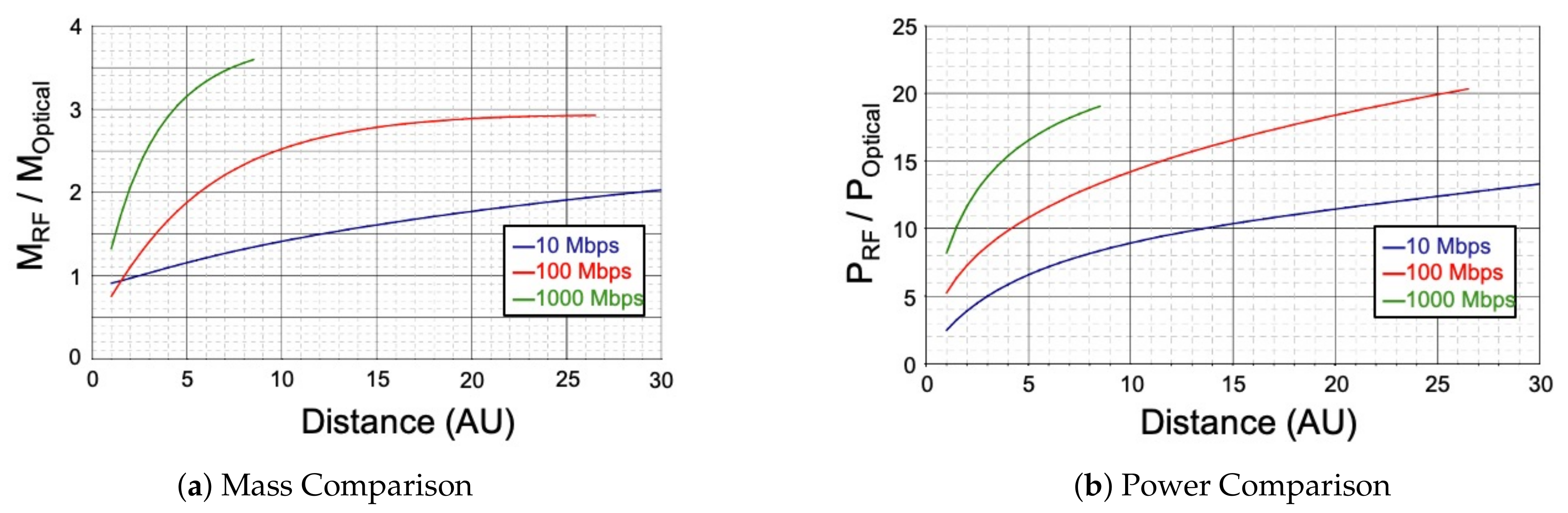
Recently, there has been a growing interest in evaluating optical communications technology for use in space systems. The Jet Propulsion Laboratory’s (JPL) Deep Space Optical Communications (DSOC) program has been developing communications systems to utilize the advantages of optical communications over its electronic counterparts [6,7,8]. Aside from the inherent increase in bandwidth provided by optical data transport, the advantage in size, weight, power, and cost (SWaP-C) also hold great potential to either miniaturize satellites or create additional space for science instruments, thereby enabling added science capabilities [9,10,11]. Figure 1a,b show a theoretical comparison of mass and power, respectively, between traditional RF and optical communications systems as a function of link distance, for various data rates [12]. Comparing the performance from the best available, space-qualified RF terminals (for the time) to the extrapolated performance of the proposed optical flight terminal that would have been used for the Mars Laser Communications Demonstration [13], showed that optical systems for inter-satellite communications can, depending on the operational data-rate, reduce the required mass by up to 3X and power requirements up to 20X! The SWaP-C for optical systems can be even further reduced by incorporating integrated photonics [14].
Intra-satellite communications can also benefit from integrated photonics. Similar to terrestrial needs, there is an increasing demand within a spacecraft to move a large amount of data between multiple on-board subsystems. Photonics can be used as the link channel to support massive data transfer with relatively high data rates [11]. Furthermore, photonics can also be used in certain systems to aid electronic operations, thereby achieve better performance (e.g., using mixers, signal generators, phase-shifters). This technique of using photonics to aid electronic operations is referred to as “microwave photonics”, and will be further discussed in Section 3.
The history and literature investigating optical communications for space systems are generally quite rich (see textbook [15]). However, research evaluating photonics, and specifically silicon photonics, for use in space systems is quite new. The present review makes a case that silicon photonics technology can enable next-generation communications systems for space, and identifies some of the challenges that need to be addressed. Section 2 gives a brief overview of some optical subsystems, and where these subsystems can benefit from using silicon photonics. Section 3 describes how microwave photonics within silicon technology can be used to aid the design of electrical space systems. Section 4 outlines the current progress of radiation effects research in silicon photonic components and systems. Finally, we summarize the review and give some suggestions for future research needs in silicon photonics for space systems.
2. Potential for Silicon Photonics in Optical Communications Systems
Flight Laser Transceivers (FLT) have been conceptualized and demonstrated in laboratories over the past several decades [16,17,18,19]. While there have been many advances in developing the technology needed for DSOC, canceled missions have delayed the demonstration and feasibility of DSOC. A notable mission that was canceled due to budgetary constraints was the Mars Telecommunication Orbiter (MTO) [20]. MTO was intended to be the first mission to demonstrate deep-space laser communications with the Mars Laser Communications Demonstration (MLCD) [21]. Target data rates were on the order of several 10’s of Mb/s during clear atmospheric conditions [22]. In 2013, the Lunar Atmospheric Dust and Environment Explorer (LADEE) that carried an FLT as part of NASA’s Lunar Laser Communication Demonstration (LLCD) was a successful mission that demonstrated free-space laser communications from the Moon [23]. While the LADEE mission was not a deep-space mission, it successfully demonstrated that laser communications from space on the order of several 100 Mb/s is possible [24,25]. Since then, there has been a new Laser Transmitter Assembly (LTA) in production, and is scheduled to fly on NASA’s mission called Psyche [7,8,26,27]. The LTA is supposed to support up to 2 Mb/s downlink rates at a distance of 2 AU (much farther than LADEE), with various modulation schemes and laser pulse widths. Mission Psyche, scheduled to launch in August 2022, will be (hopefully) the first mission to demonstrate the feasibility of DSOC, provide further proof of the need for DSOC for future missions, especially for human spaceflight, and also reveal some challenges that could open doors to further research and development in DSOC.
In parallel, however, the development of silicon photonics in the terrestrial telecommunications sphere has opened the door for its potential use in upgrading FLTs. So while the DSOC demonstration with mission Psyche is ongoing, research and design efforts focused on using silicon photonics to replace some parts of the FLT to gain SWaP-C advantages can commence.
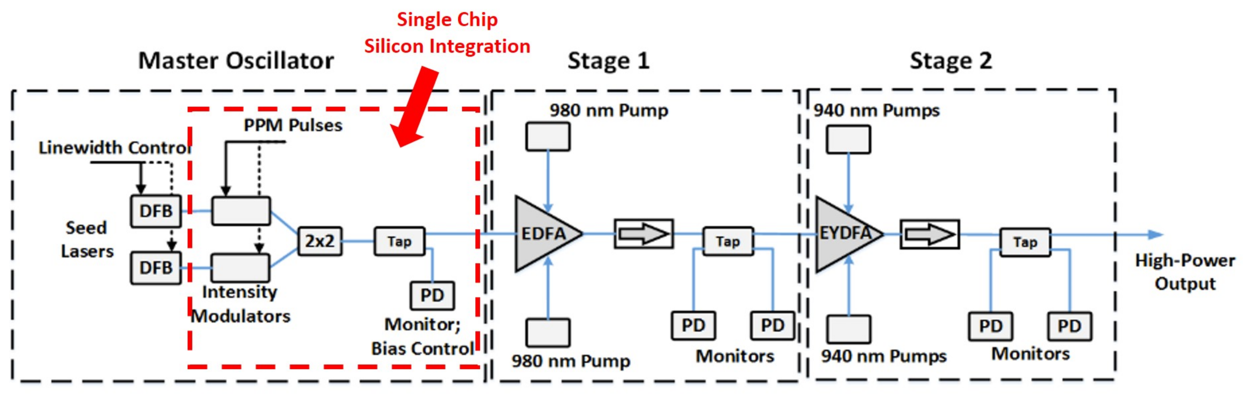
One of the main constraints limiting space systems is size and weight. Miniaturization of any system component, preferably without the loss of performance and functionality, is highly desirable. Smaller footprints lead to decreased costs in fuel consumption and the potential to include other systems that would otherwise not be able to fit within a spacecraft. Silicon photonics can be used to substitute discrete commercial off-the-shelf (COTS) components that take up a significant amount of space, to smaller integrated components on a single silicon die. For example, shown in Figure 2 is a top-level architecture of the LTA described in [26]. In this system, the master oscillator block contains a distributed feedback (DFB) laser that provides a continuous optical signal that is modulated by an intensity modulator to convert electrical data into optical data. There are two of each (for redundancy) to minimize the number of single points of system failure. Since only one of the DFBs is in use at any given time, the optical signal is routed to a single link through the 2 × 2 block. An optical tap and photodiode (PD) are used in the signal link to monitor the signal integrity and provide feedback for optimum bias control. This LTA is designed to output a 1550-nm pulse-position modulation (PPM) communications scheme. In its current form, the intensity modulators, 2 × 2 coupler, tap, and PD are all discrete COTS components. While silicon, for the most part, cannot provide the requisite lasing at 1550 nm, all of the other components can be integrated onto a single silicon chip, as outlined in the dashed red box in Figure 2. Furthermore, what is not shown is the necessary electronics that take the digital data and produce the electrical PPM signal. These components, which include the digital-to-analog converter (DAC), pulse shaping filters, and the electrical drivers that are needed for the intensity modulators, can also be integrated on the same silicon chip, massively reducing the necessary form-factor. An example of a terrestrial all-silicon optical transceiver that achieves a high-density integration of optical and electrical components with comparable performance was demonstrated by Narasimha et al. [28]. Similar techniques can be used to condense the LTA design into a smaller footprint. However, it should be noted that this modulator achieves roughly 4 dB optical extinction ratio. In comparison, an LTA needs >33 dB pulse extinction ratio to meet flight requirements. While this might seem like a huge technology performance gap, silicon optical modulators have not been optimized for space systems where such a high extinction ratio is needed. Some designs have improved the extinction ratio (∼18 dB) [29], but more focused design efforts are still needed to meet flight requirements.
Temperature control for silicon systems is also important to consider for space systems. For example, silicon modulators’ bias point can shift with changing temperature. However, many silicon modulators are designed with on-chip thermal tuners to provide DC bias control, and retain their modulation efficiency across temperature [30,31,32]. While the heater does tend to raise the power consumption of the modulator, it is only on the order of several mW, and thus, is not a huge concern from a power and size perspective.
The LTA in Figure 2 has two subsequent stages that use fiber amplifiers to boost the optical output power. These amplifying stages also relax the insertion loss constraints imposed by the modulator. While in theory some of these components can also be integrated in silicon (e.g., the taps and PDs), the optical power is typically too high (>23 dBm) to be supported by integrated waveguides due to potential non-linear optical effects [33].
Overall, the development and maturation of silicon photonics can result in a large reduction in size and weight for space optical systems. The integration approach can further reduce the size constraints by limiting the need for individual component packaging and removing unnecessary electrical and optical interconnects between components.
3. Microwave Photonics
Beyond the numerous advantages integrated silicon photonics brings for SWaP-C benefits for optical communication in space, they also can be used to add new capabilities or enhance our conventional radio-frequency (RF) communications systems. To this end, the field of microwave photonics aims to use photonic devices and their unique properties to implement RF functionality over optical fiber links. In order to understand the benefits integrated photonics can bring to RF communications systems, it is important to understand the traditional limitations of conventional electronics. With conventional electronics, circuits and systems are often designed to operate over narrow bandwidths. This is due to the large challenges associated with the frequency response and nonlinearities of integrated active devices. Although there are several techniques that have been shown to overcome the bandwidth limitations [34], this increases design complexity and the device nonlinearities still persist. These device nonlinearities result in low-frequency tuning range in frequency synthesizers, numerous spurious tones in the output spectrum of RF mixers for up and down-conversion, and phase errors in RF phase shifters.
In particular, for space-based applications, a significant challenge for RF communications systems is carefully handling low signal-to-noise ratio signals. In an electronic system, the minimum detectable signal is determined by the bandwidth of interest and the receiver noise performance. With conventional electronics, the receiver noise performance comes at a tradeoff with bandwidth or power consumption. The consequence of this tradeoff is that the achievable data rate and possible types of modulation schemes of the electronic system become limited by the dynamic range of the receiver. In contrast, photonic components present promising alternatives to overcome the limitations in electrical communications systems for space-based applications. An important benefit of photonic components for RF communications systems is the high spurious-free dynamic range (SFDR) of integrated modulators [35]. This allows for spectrally pure communications which can improve the detection of weak signals. In addition, as the optical carrier lies at a frequency significantly higher than the desired RF frequencies, the fractional bandwidth is small. This allows wideband RF communications to be supported through the optical signal chain.
The extensive applications of microwave photonics can be found in [36]. In this section, special focus will be given to key transceiver building blocks and new directions that benefit from integrated electronic-photonic technology platforms.
For RF mixers, the microwave photonic equivalent circuits provide several advantages. As mentioned earlier, the high bandwidth processing capability of photonic components allows microwave photonic mixers to perform over wide RF and intermediate frequency (IF) bandwidths. At the same time, due to the translation from the electrical to the optical domain, the port-to-port isolation on the mixer will be high, allowing for a clear spectrum at the output. Furthermore, the high dynamic range capability of silicon photonic modulators is especially important for RF mixers that are used for frequency conversion, which are prone to generating substantial spurious content. The works in [35,37,38] demonstrate the design of high SFDR microwave photonic mixers. In [35], an integrated silicon photonics platform is utilized and demonstrates an SFDR of 92 dB/Hz.
Another important block for RF transceivers is the phase shifter, which is used in beamforming networks to direct and steer RF power at the antenna. Traditional electrical phase shifters rely on nonlinear components such as varactors, transistors, or electrical filters to achieve phase-shifting However, both of these approaches result in band-limited performance. Microwave photonic equivalents, on the other hand, have the ability to generate phase shifts over relatively higher bandwidths. The work in [39] implements a microwave photonic RF phase shifter operating across a 10–16 GHz and 36–42 GHz frequency range in a silicon-on-insulator technology. The optical phase shifter is implemented using a silicon rib waveguide with an interdigitated pn-junction. With this structure, a phase shift is achieved by applying reverse bias onto the pn-junctions, which changes the effective index on the waveguide, producing a phase shift in the optical signal. Since this process is analog it allows for continuous tuning, rather than discrete steps. The authors in [39] demonstrate a linear 475 phase shift with the precision of 0.06/mV over the 0 to 8 V bias tuning range.
Signal generation is another important building block for RF transceivers. In a conventional electrical system, an electronic oscillator is designed to accomplish this. The main specification in such a design is the phase noise of the oscillator. At the same time, for use in a frequency synthesizer, the tuning range of the oscillator is also important. In comparison, lasers have high-frequency agility and notably lower noise when compared with an electronic oscillator. To exploit these features, photo-mixing can be used to generate the desired RF tone. In photo-mixing, two wavelengths are mixed together in the photodiode to generate the beat frequency of the two wavelengths. In this way, a microwave signal can be generated in the electrical domain. This feature has been used in [40,41]. In [40], an array of photodetectors was connected to electrical antennas where the radiated tones could be measured. In this case, the array operates from 21 to 65 GHz, limited on the low end by the antenna frequency response. In [41], a dual-fed photodetector was used to generate high power over a 40 GHz bandwidth. In that work, 12.3 dBm and 5.3 dBm was generated at 2 GHz and 40 GHz, respectively.
A new design arena, unique to integrated electronic-photonic technologies, is that of co-designed electronic-photonic microwave photonic systems. In this instance, the benefits of electronics and photonics can be combined, without the overhead and constraints introduced by packaging. An example of this was demonstrated in [42]. In that work, an electronic Colpitts oscillator was designed in a 250 nm electronic-photonic SiGe BiCMOS technology platform. That oscillator takes advantage of an injection locking mechanism of oscillators by using photodiodes and photomixing to inject a generated microwave photonic tone into the oscillator. In this manner, the phase noise of the electronic oscillator, which operates at twice the frequency of the microwave photonic tone, can be reduced and approaches that of the microwave photonic injected signal. In that work a 58.5 GHz signal was generated with phase noise of dBc/Hz at 1 MHz offset from the carrier. Another example of this co-design arena can be found in [43]. In that work, the advantages of the robust distributed amplifier electronic architecture were combined with photo-mixing to generate a wideband high power signal source. To accomplish this, a distributed amplifier using SiGe HBT-based amplifier cells was merged with a distributed photodiode array. In this way, the power from each photodiode is amplified by the amplifier and then combined in phase in the electronic domain. In that work, a power of 10 dBm was generated across a 50 GHz bandwidth. For space-based applications, where communication can be spread amongst several frequencies, the high-frequency agility of this amplifier can eliminate the need for multiple transmitters for different frequency bands that would have been needed with a purely electrical solution. The previous examples focus on photo-mixing and take advantage of the spectral purity of the optical sources. However, another demonstrated approach in [44] was focused on the linearization of an RF receiver. In that work, a distributed low noise amplifier was co-designed with an MZM. To compensate for the nonlinearity of the modulator, the distributed amplifier used an intermodulation injection scheme which was shown to boost the SFDR of the receiver. That design leveraged the ability to create wideband, nonlinear sources which can be used to compensate for photonic component nonlinearities. In that work, an SFDR greater than 109 dB/Hz was demonstrated over a 19 GHz bandwidth. These benefits can be extended to space-based applications to enhance the detection of received signals. From all of these examples, it can be seen that the emerging design arena of co-designed electronic-photonic systems has great potential for enhancing microwave communications systems. In addition, with electronics and photonics integrated into the same technology monolithically, new topologies, which would have been infeasible in a multi-chip solution, can be developed.
4. Space Radiation Effects
The space environment contains a plethora of complex radiation phenomena, ranging from galactic cosmic rays that can cause single-event effects (SEE), to high-energy solar particles that can cause total-ionizing dose damage (TID) and displacement damage (DD) in semiconductor components [45,46,47,48,49,50,51,52]. All radiation effects present reliability concerns for space systems, which makes silicon photonics potentially vulnerable to space radiation. The extent to which radiation can impede the functionality of a component depends on the radiation source (e.g., high-energy ion versus high-energy gamma), and the underlying operation physics of the component itself. Knowledge of how various components respond to radiation phenomena is important when considering a system’s survivability in the space environment. It can also provide insight into radiation-hardening methods to make certain components more robust to specific types of radiation. This section gives an overview of the current progress of radiation effects in silicon photonics. As a reference for radiation levels, near-Earth space models for TID exposure, depending on the orbit of the spacecraft, suggest roughly 10–100 krad(Si) per year, while missions to Jupiter could experience radiation levels as much as several hundred krad(Si) over the entire mission lifetime for components that are within a radiation vault, and 50 Mrad(Si) for components outside of this vault [53,54]. DD radiation damage is mostly caused by protons in space which, in near-Earth models, can reach fluxes of cms for energies >10 MeV [45,46,50]. However, since protons cause both TID and DD damage, it is preferable to test DD with neutrons to decouple these radiation effects, as neutrons only cause DD damage. The relationship between damage caused by neutrons to that of protons can be approximated by the non-ionizing energy loss (NIEL) scaling hypothesis and can be found in [55,56]. For proton and neutron energies >10 MeV, the NIEL scaling is similar, which allows for proper DD testing with neutrons (which is the case for the DD studies presented in this review). Finally, the abundance of high-energy particles in our solar system that cause SEEs is quite dynamic based on our sun’s activity and the element in question. However, heavy-ion models, such as CREME96 [57], can be used to capture these dynamics and predict the flux of ions such as H and Fe with maximum levels of and (cm-s-sr-MeV/nuc), respectively. For a more in-depth analysis of space climatology, the interested reader is directed to [45].
4.1. Integrated Germanium Photodiodes
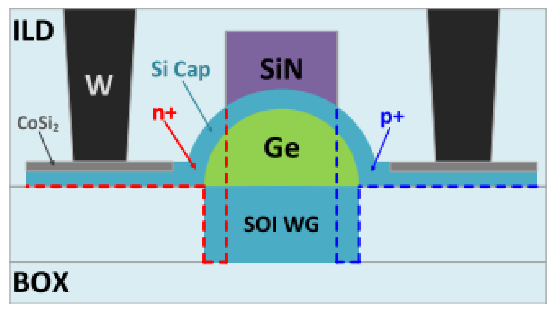
Integrated bulk germanium photodiodes (PD) are used as the main optical-to-electrical converters in silicon photonic systems [58,59,60,61]. The photodiode relies on a p-i-n junction within the bulk germanium to collect photo-induced free carriers. Shown in Figure 3 is a typical structure of an integrated germanium PD [58,62]. A reverse-bias voltage is applied to the PD through the tungsten contacts to create a strong electric field in the germanium region. Light incident from the silicon waveguide, normal to the structure in Figure 3, with photon energy 0.8 eV will get converted to free carriers as photo-current. TID, SEE, and DD radiation effects investigations have been conducted to determine if this standard operating working principle of the PD is, in any way, altered.
4.1.1. Photodiodes: Total-Ionizing Dose Effects
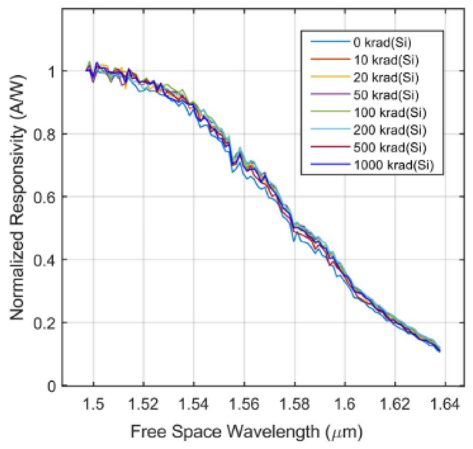
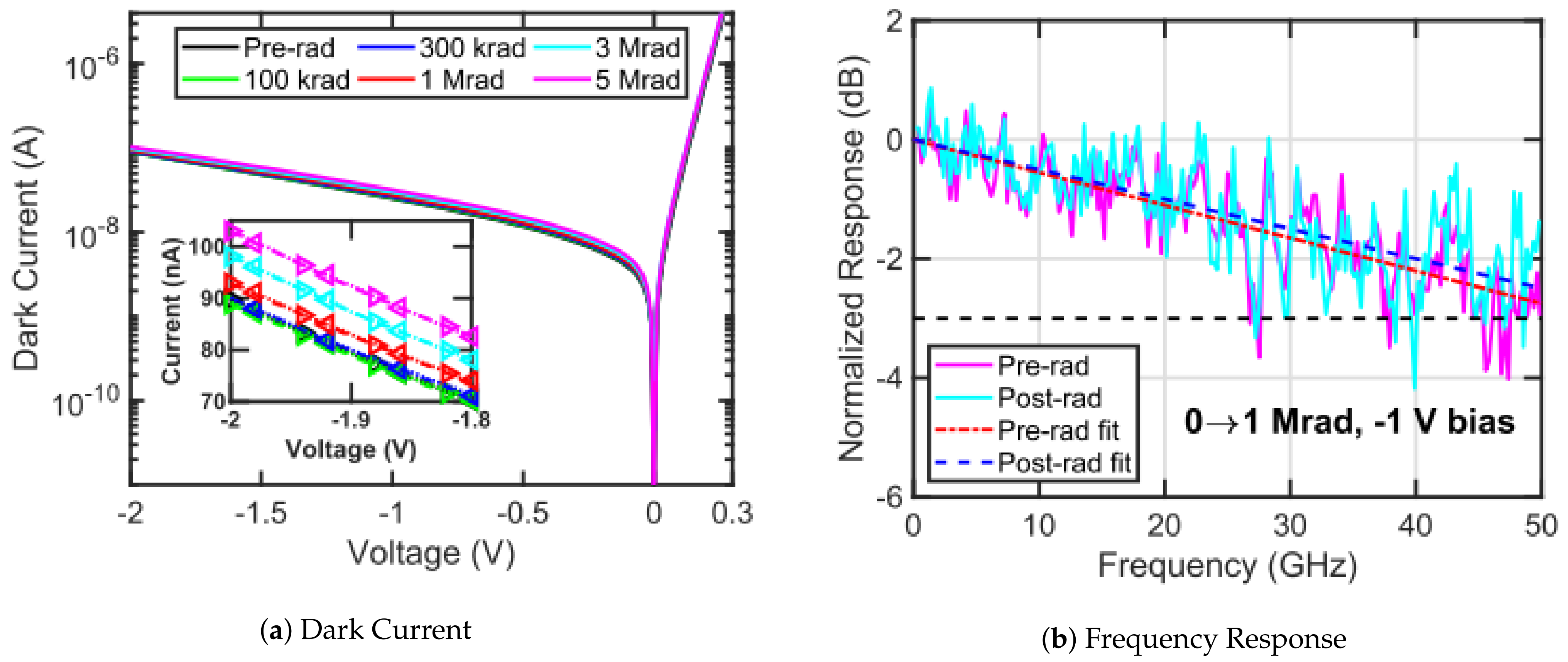
It has been shown that TID does not significantly affect integrated germanium PDs [62,63,64]. Figure 4 shows negligible change in responsivity up to 1 Mrad(Si) [64]. The resistance to TID has to do with the fundamental mechanism associated with the generation of TID-induced damage. TID adds positive charge to insulators and creates traps between semiconductor-insulator interfaces. It is expected then, that devices which exhibit charge transport near insulator interfaces (e.g., field-effect transistors) will be especially vulnerable to TID. However, the PD’s charge transport path is within the bulk of the i-region where the photo-generated carriers originate. In other words, TID-induced damage on the interfaces should have minimal effect on the device’s ability to convert photons to electrical carriers.
The dark current and AC response were also shown to suffer negligible degradation from TID damage. Figure 5a shows only small resultant increases in dark current post-irradiation [62]. However, this small increase could be due to the thermal heating of the p-i-n junction from X-ray radiation, and not the actual damage inflicted on the device. Figure 5b compares the 3-dB optical-to-electrical bandwidth, both before and after irradiation. The small difference in the fit was attributed to the measurement tolerance of the equipment, and the study, therefore, concluded that there was no device performance change due to TID. The PD capacitance and resistance were also measured and showed no differences.
4.1.2. Photodiodes: Displacement Damage Effects
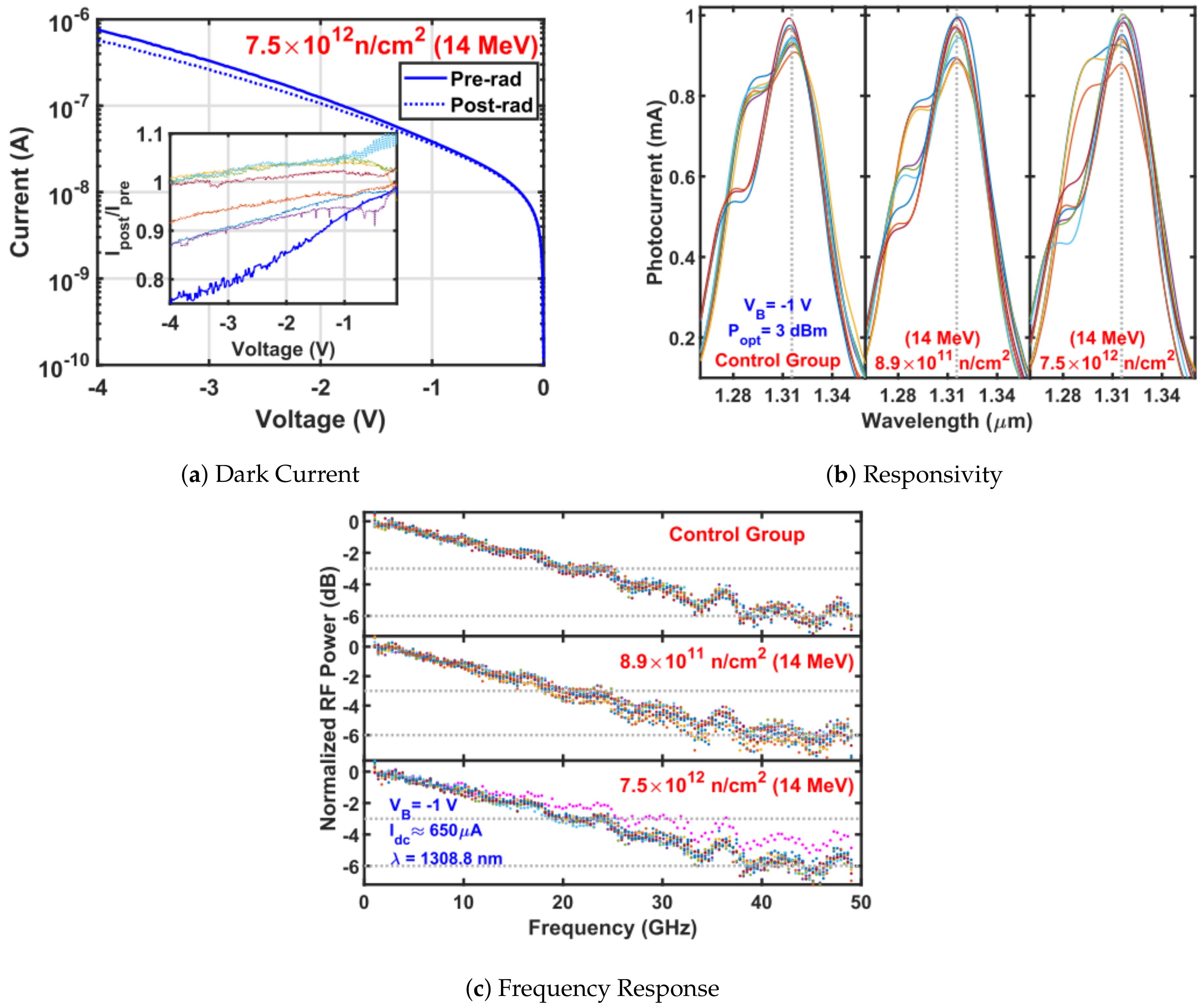
Section 4.1.1 demonstrated that since TID mostly relies on an interface damage mechanism, it does not have much of an effect on bulk-transport Ge PDs. However, a logical question presents itself: does radiation that produces bulk damage have a significant effect? The only experiment, to date, that has been conducted to answer this question suggests that even DD effects have minimal impact on PD performance [65]. This experiment exposed several PDs to 14 MeV neutrons, up to a fluence of 7.5 × 10 neutrons/cm.
These results suggest that dark current is largely unchanged by DD, as shown in Figure 6a. The lack of damage is attributed to the fact that the pre-irradiation bulk trap density is already fairly large in such devices. The high trap densities are a direct consequence of fabricating a lattice-mismatched Ge crystal onto silicon. As a result, the neutron-generated bulk trap density is not enough to overcome the pre-existing density of bulk traps.
The responsivity and optical-to-electrical bandwidth are also shown to have no change due to DD: Figure 6b,c, respectively. Responsivity does not change significantly because the carrier collection processes in this PD are primarily drift-based, which is less sensitive to bulk traps than diffusion-based charge transport. The bandwidth was also shown to not degrade with increasing neutron dose. A change in the junction capacitance was observed as a direct result of radiation, but it is of little concern, since the PD’s bandwidth is limited by the carrier transit-time, as opposed to capacitive charging.
4.1.3. Photodiodes: Single-Event Effects
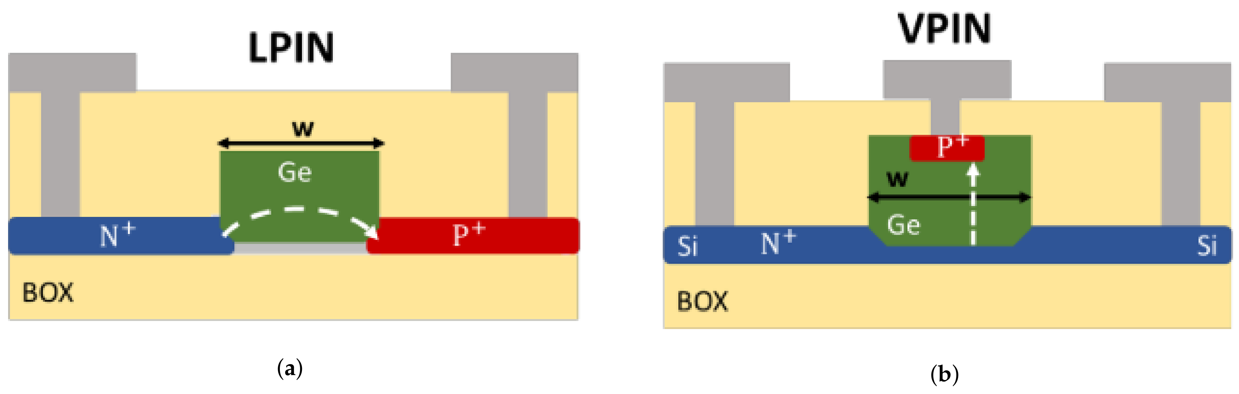
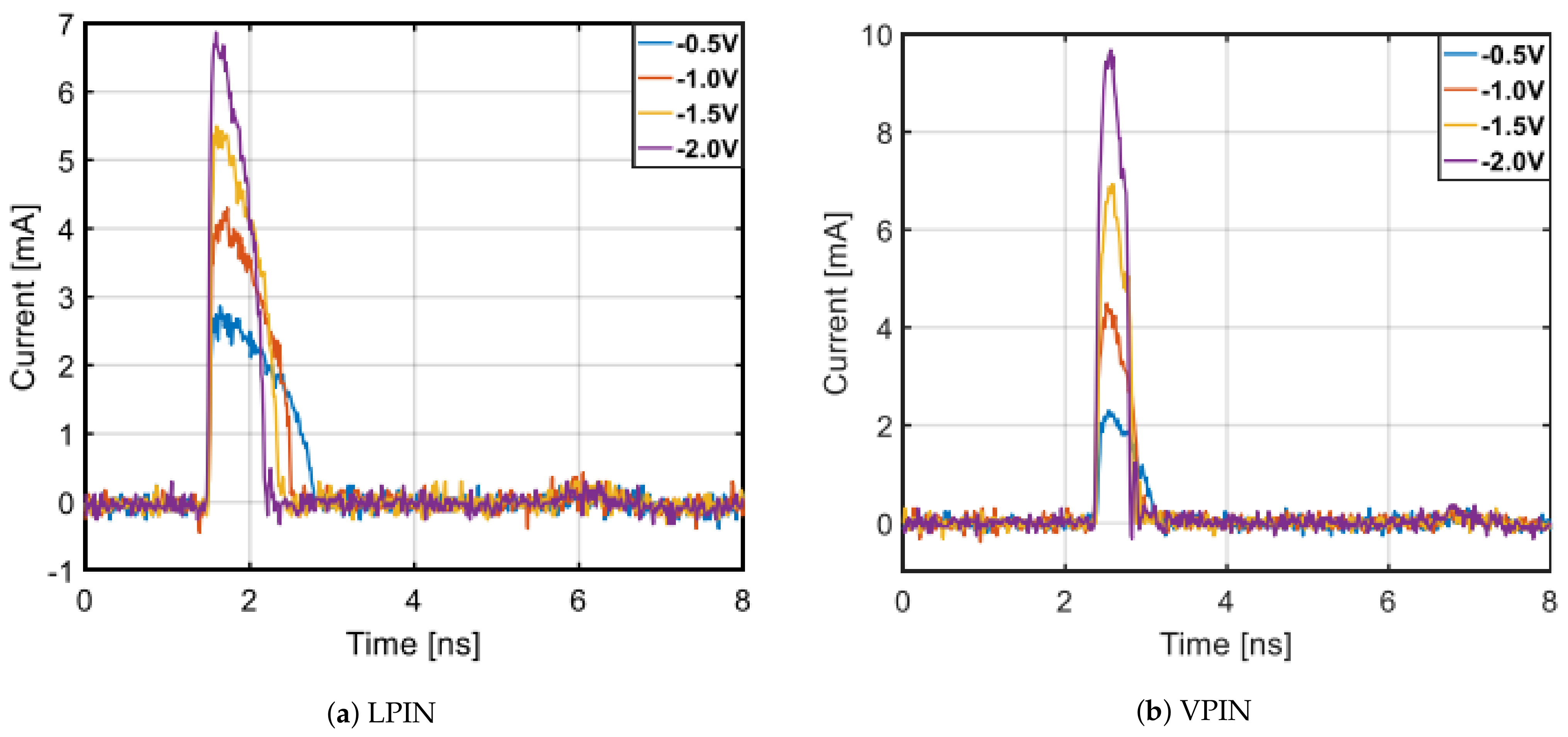
SEEs are caused by a high-energy particle imparting its energy to the crystal lattice, thereby generating a high density of electron/hole pairs (EHPs). This process creates current transients that can corrupt data encoded on the optical signal. There has only been one investigation, to date, that discusses the transient effects in lateral and vertical p-i-n PD, as shown in Figure 7a (similar to the one shown in Figure 3) and Figure 7b, respectively [66]. A high-energy laser pulse was used to induce transients in the PDs. Figure 8a,b show the resulting current transients for a lateral and vertical p-i-n PD, respectively, induced by a 500-pJ laser pulse. The transient increases in magnitude with a larger reverse bias, for both cases. This is because the electric field within the junction increases and is able to separate and collect more EHPs, resulting in larger current spikes.
The transient duration, however, appears to only depend on reverse-bias voltage for the lateral device. This phenomenon is attributed to the fact that the electric field in the lateral device (depicted by the dashed arrow in Figure 7) is strongest near the buried oxide (BOX), and decreases toward the top of the Ge layer. Therefore, the carrier transit-time is non-uniform and strongly dependent on the magnitude of the reverse-bias voltage. The vertical p-i-n PD, in contrast, has a much more uniform electric field throughout the Ge layer. The study also claims that the electric-field magnitude in the vertical p-i-n is much higher than its horizontal counterpart, even at low voltages. Carriers in the vertical p-i-n accelerate to near saturation velocity which results in a weak dependence in transient duration to reverse-bias voltage.
Typically, a transient with a small peak and short duration is desired in order to reduce the probability of data corruption. This investigation showed that there is a trade-off between these two transient characteristics: the horizontal p-i-n has a smaller peak magnitude, while the vertical p-i-n has a shorter transient duration. In this case, transients need to be examined from a system perspective to determine which structure is more desirable for reducing the probability of bit errors in a heavy-ion rich environment. Parameters such as bit-rate, modulation type, and modulation depth are just a few things to consider when evaluating this trade-space.
As a final note on this study, it is relatively unclear how transients induced by a laser pulse in a laboratory compare to transients induced by high-energy ions, as you would see in space. An important distinction is that the laser pulse generates most of the EHPs within its ∼1 m spotsize. This is much larger than a high-energy ion, which could have an EHP generation radius on the order of several tens to hundreds of nanometers. Several studies have been conducted to compare and contrast laser- and ion-induced transients in electrical devices [67,68,69,70,71,72,73,74]. While there have been some successes in developing techniques to correlate and predict the corresponding transient response from a particle, it is clear that this correlation varies between different technologies, materials, and operating device physics. Therefore, the correlation between laser- and ion-induced transients in silicon photonic devices remains an area of research yet to be addressed.
4.2. Integrated Silicon Waveguides
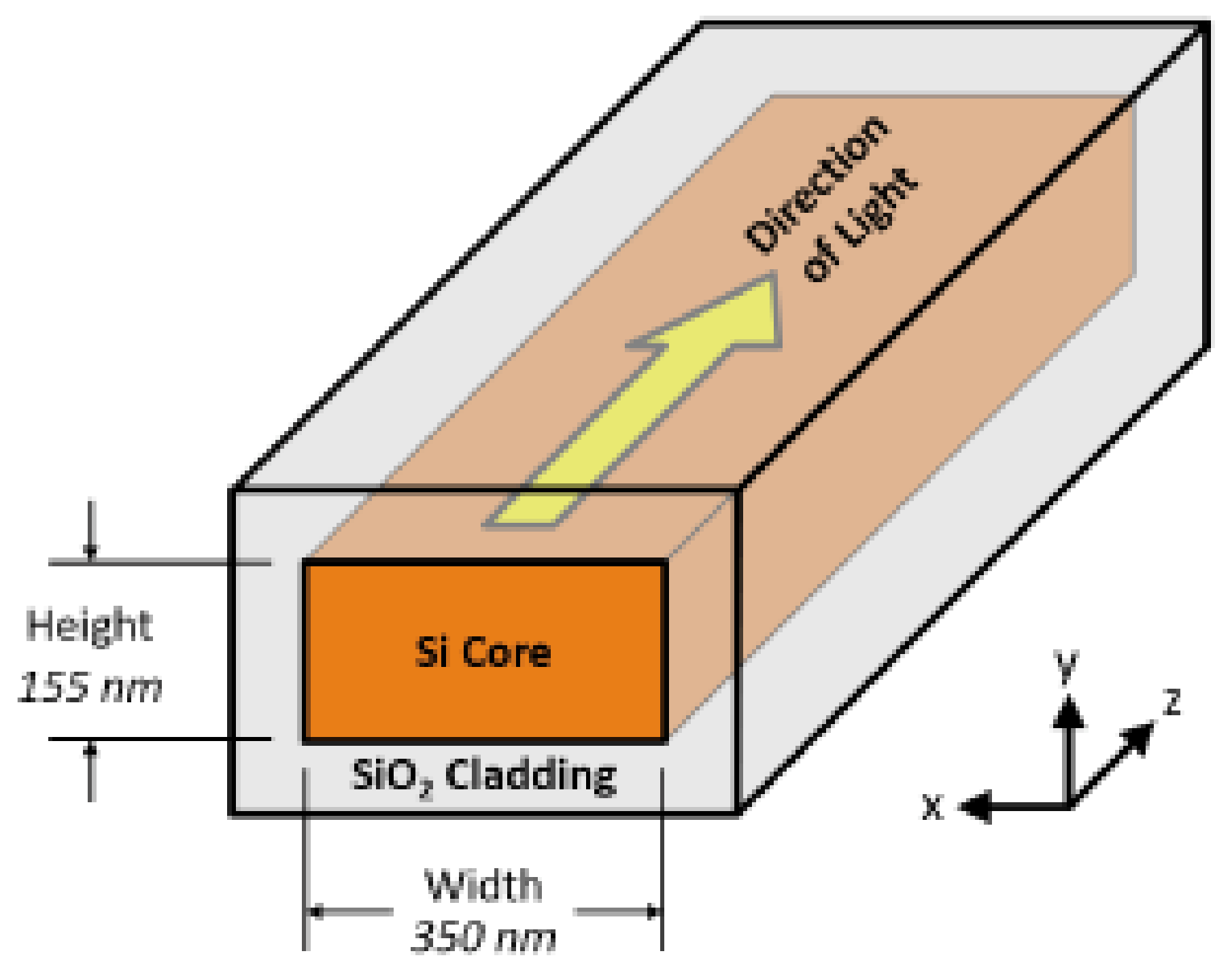
Silicon waveguides move light between two points of interest, in a manner similar to how metal conductors move electrical signals. This function makes waveguides ubiquitous in silicon photonic systems, and they come in various shapes and sizes depending on the optical wavelength and other parameters, such as loss and confinement [75]. An example of a waveguide with nominal dimensions and basic operation is shown in Figure 9 [4,76]. It confines light to its silicon core through the index of refraction difference between the oxide and the silicon. Low loss and low dispersion are typically desired. Radiation that alters this basic functionality must be considered when designing silicon photonic systems.
4.2.1. Waveguides: Total-Ionizing Dose Effects
The silicon waveguide core is surrounded by an insulator, which makes it potentially vulnerable to TID. Generating trap states on the interfaces could negatively impact the optical transmission properties. The lack of an electric field in the waveguides, however, does reduce the charge yield, and thus the resulting radiation damage [77]. Two studies that exposed silicon waveguides to a high-dose gamma radiation confirm that the waveguide maintains its transmission properties after irradiation [78,79]. These results suggest that the charge yield from radiation is low in these components, and that the optical mode within the waveguide is negligibly affected by this type of damage.
4.2.2. Waveguides: Displacement Damage Effects
No direct investigation has been conducted to determine if bulk defects cause significant transmission loss in silicon waveguides. However, the study in Goley et al. [65], which irradiated p-i-n PDs with 14-MeV neutrons to a fluence of 7.5 × 10 neutrons/cm, used a silicon waveguide to guide light to the photodiode. Since no radiation-induced performance degradation was found with the photodiode, it can be inferred that the waveguides used in that study also did not exhibit any substantial DD effects.
4.2.3. Waveguides: Single-Event Effects
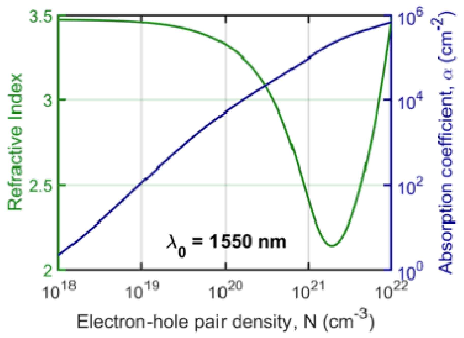
SEEs in silicon waveguides were theoretically proposed to be a potential source of concern for space systems [80]. An energetic particle can generate a dense cloud of free carriers within the waveguide such that light traveling through this cloud can be absorbed through free-carrier absorption. Figure 10 shows the refractive index change and the absorption profile for different densities of induced EHPs within the waveguide for 1550-nm light [81]. Heavy ions that generate a substantial amount of EHPs can increase the absorption coefficient of the waveguide by several orders of magnitude, which can disrupt the optical signal. The induced EHP density also impacts the refractive index, but the change is too small and the lateral charge track is too narrow, to produce any severe phase effects.
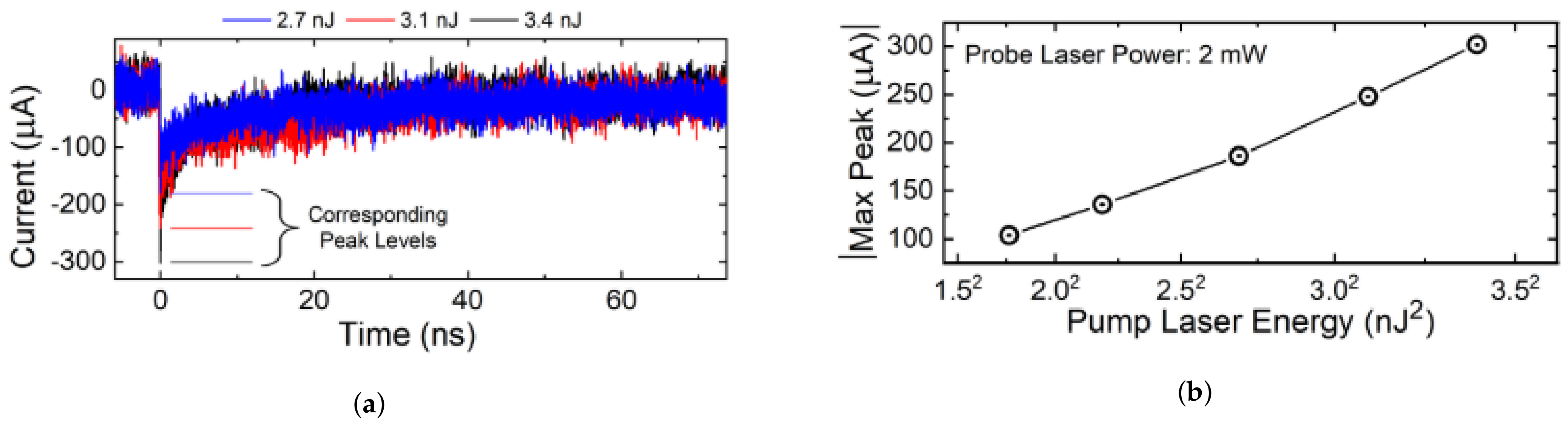
This theory was tested experimentally by inducing a dense cloud of EHPs in a waveguide through the two-photon absorption process using a high-energy laser pulse [76]. It was confirmed that when free carriers are present within the waveguide, a fraction of the optical signal is depleted. Figure 11a shows the transient results from an optical signal passing through an induced cloud of EHPs. The y-axis shows the AC-coupled portion of the PD current induced by this perturbation measured via a bias tee. Note that with increasing pulse energy (i.e., the larger density of induced EHPs) the transient peak increases. A collection of transient peaks with respect to laser energy is shown in Figure 11b. This is consistent with the theoretically predicted results by Goley et al. [80]. Historically, a subset of SEEs termed single-event transients (SET) have been observed in electronic parts. In this case, however, the transient exists purely in the optical domain, where no charge collection is taking place and is distinctly different than any other SET. Thus a new type of SEEs that encompasses the present phenomenon is needed, and is termed the optical single-event transient (OSET). An OSET is defined as the “perturbation of optical power within an integrated optical component that strictly exists in the optical domain and does not affect the functionality of any electronics that precede it” [76].
Due to experimental limitations with the TPA process, a maximum transmission loss of ∼15% was measured. However, simulation results from Goley et al. [80] and Tzintzarov et al. [76] predict that 100% transmission loss is possible. This loss can be detrimental to optically modulated data during an ion strike, leading to bit errors and instantaneous drops in a communication link.
4.3. Mach-Zehnder Modulators
A Mach-Zehnder modulator (MZM) is an electrical-to-optical (E/O) converter topology commonly used in photonic transmitters. It utilizes the plasma dispersion effect to alter the phase of the optical signal [82], and a two-arm topology to convert phase modulation to amplitude modulation via constructive and destructive interference [83]. The understanding of the various forms of radiation effects is still in its infancy for MZMs. To date, several TID and DD studies have been conducted, but, to the authors’ best knowledge, no studies with SEEs exist in the literature.
4.3.1. MZM: Total-Ionizing Dose Effects
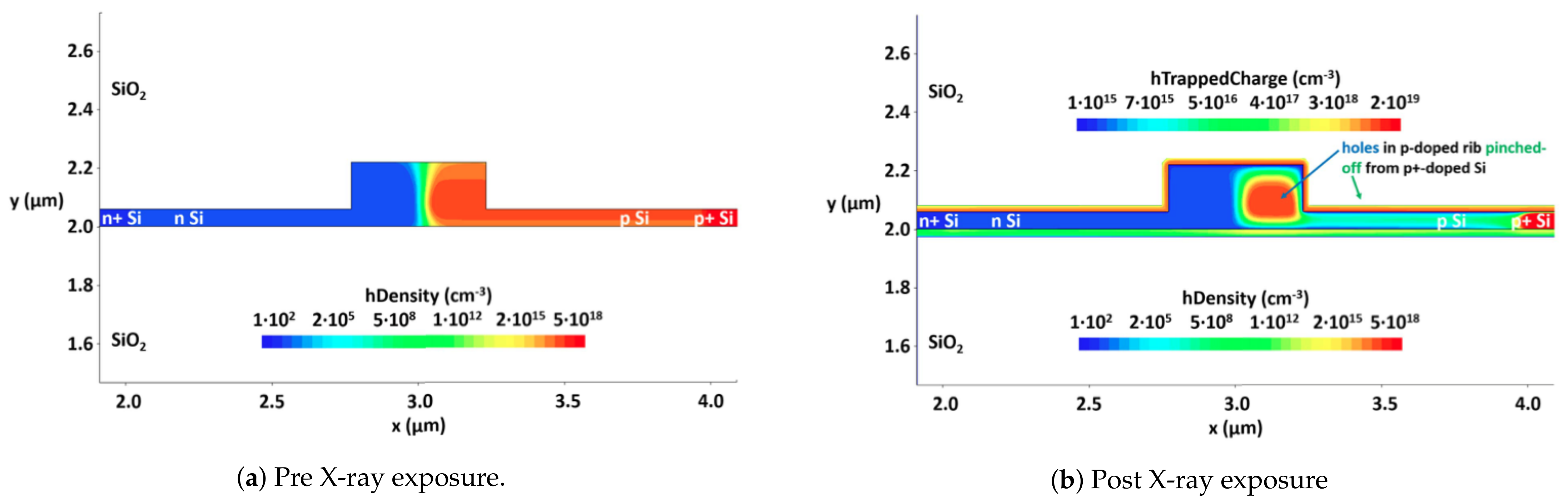
It was first noticed that relatively high doses (∼1.3 MGy) of radiation can completely render an MZM useless (i.e., an inability to modulate light) [84]. The reason for this was later attributed to a “pinch-off” effect that begins to form on the p-side of the modulator [85]. Shown in Figure 12a,b are cross-sections of the modulator pre- and post-250 kGy of radiation, respectively [63]. Note that the carrier concentration on the p-side of the modulator is reduced by several orders of magnitude. This reduction is produced when TID positively charges the oxide and pushes the free carriers out of the arm, losing the electrical connection between the contact and the intrinsic modulator. Without this connection, the modulator can no longer function as intended.
To try and mitigate the pinch-off effect, Zeiler et al. showed that a shallow etch, and/or higher contact doping in the modulator can make it more tolerant to TID [63]. A shallow etch (i.e., thicker SOI), means that a larger dose would be required to deplete the carriers and fully disconnect the p-side contact. Larger doping on the p-side arm makes it harder to fully deplete the carriers, which also results in a more radiation-tolerant modulator.
4.3.2. MZM: Displacement Damage Effects
Two prevalent studies that bombarded an MZM with 20-MeV neutrons up to 1.2 × 10[84] and 3 × 10 neutrons/cm[63] confirm that the modulator shows no change in modulation efficiency and bias control. Radiation tolerance to neutrons is attributed to the high doping levels used in the modulator. The modulators for these studies have doping levels on the order of 1 × 10 to 1 × 10 cm[86]. Assuming that the defect density caused by the neutrons is on the same order of magnitude as the neutron fluence, then 3 × 10 neutrons/cm fluence would result in roughly 3 × 10 cm induced defect density, which is an order of magnitude lower than the doping level [56]. The difference between damage and doping levels suggests that the neutron fluence is not large enough to damage an MZM in any significant way. Therefore, it can be concluded that MZMs should be reasonably robust to DD effects.
4.4. System Integration Considerations
One important factor to consider with silicon integrated systems that include both electronics and photonics is the radiation impact, or propagation, from the electronic to photonic domain. This monolithic, system integration aspect adds an entirely different set of radiation effects to silicon photonics, ones that come from the electronics domain. The good thing is that there have been over 40 years of radiation effects research in silicon electronics. However, the literature is fairly sparse when it comes to combining the radiation effects from electronics and photonics.
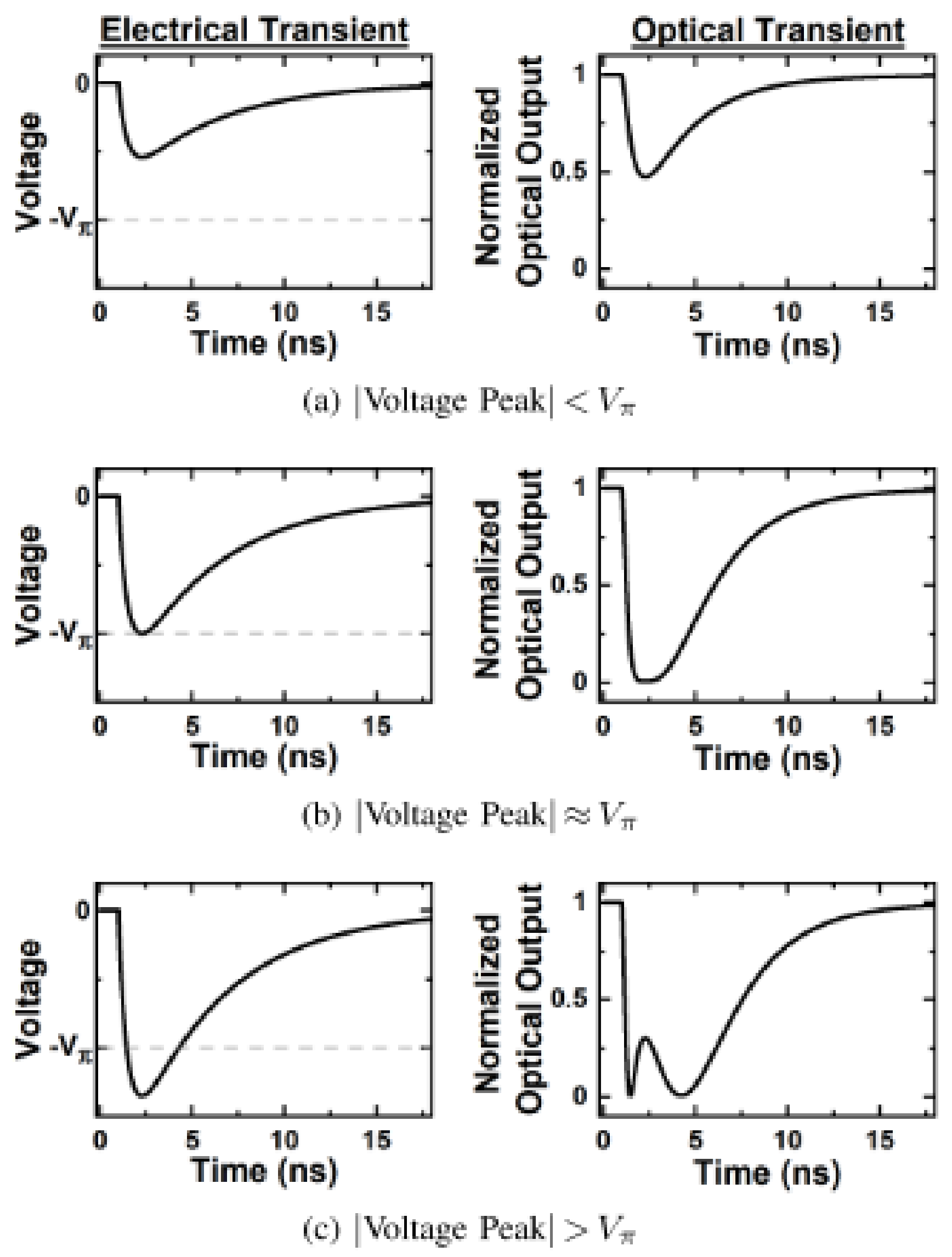
One study attempts to describe how SETs that are generated within a SiGe bipolar-based driver propagate into the photonic domain [87]. An important result from this work is that the resulting optical transients are dependent on the magnitude of the electrical transient relative to the V parameter of the modulator, as shown in Figure 13. An electrical transient with a peak magnitude of V will result in an optical transient that fully depletes the optical signal, potentially causing bit errors and degradation in the system. Furthermore, since V can be tuned based on doping and length of the phase shifters used in an MZM, a designer has the option to build a modulator that can be arbitrarily robust to SETs.
This study suggested that there can be other design methodologies to harden silicon photonic systems. In other words, even electronics that can be highly vulnerable to various radiation effects can be compensated on the system level when photonics are brought on-board. Regardless, more SEE, TID, and DD investigations must be performed to obtain a complete picture of all of the design techniques that can be used to harden integrated silicon photonic systems.
4.5. Radiation Effects: Takeaways
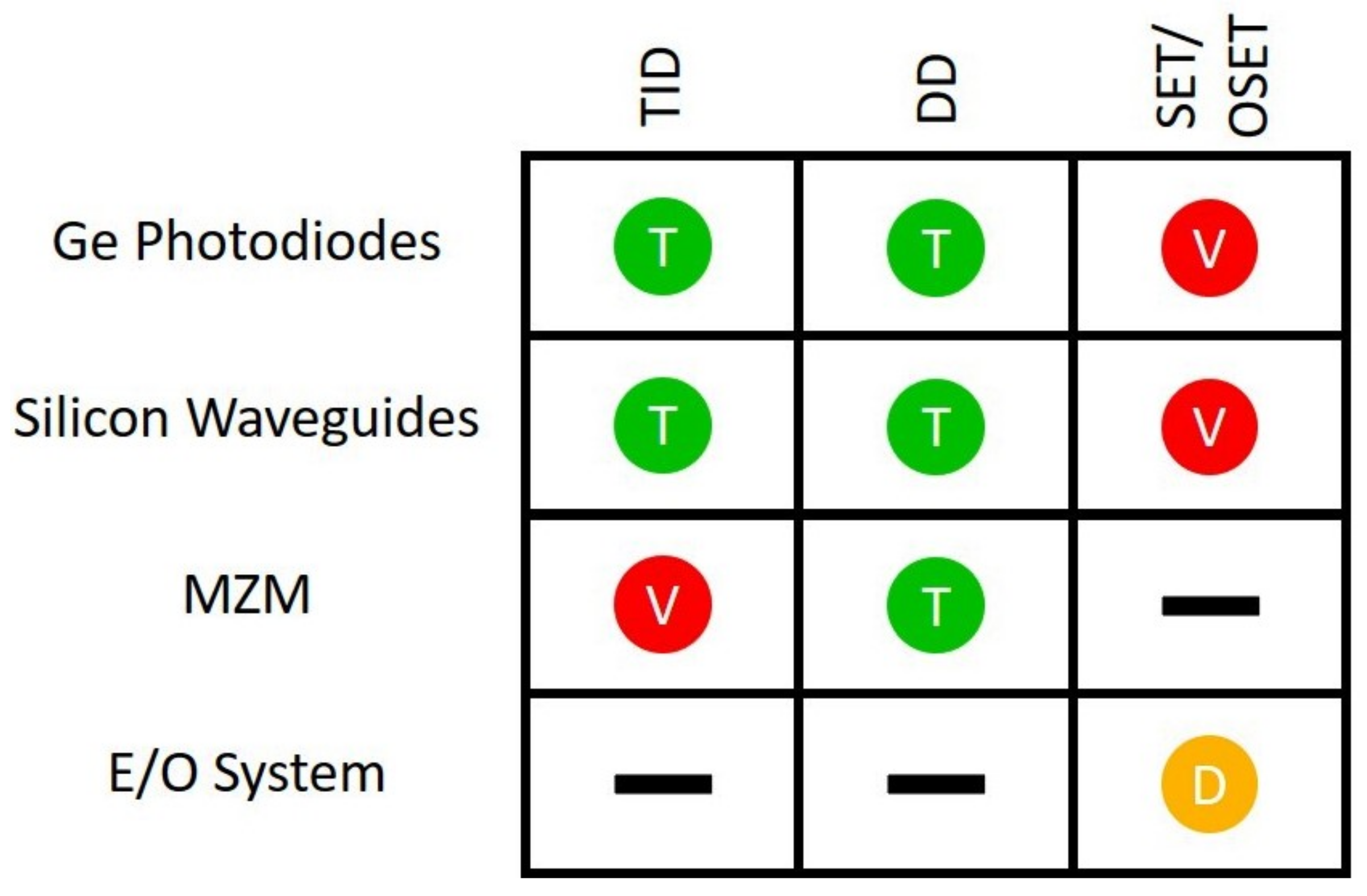
The field of radiation effects in silicon photonics is, as we have shown, still quite young. A summary of the current work in this field showing some of the devices’ vulnerabilities and tolerances to radiation is presented in Figure 14. TID and DD effects seem to pose fewer concerns for silicon photonics in space. SETs, on the other hand, have shown to quite problematic. It is difficult to say with certainty whether an SET/OSET will present serious concerns, since they have to be looked at from the system level and analyzed with various modulation schemes and other variables. The black lines in Figure 14 signify that there is currently no research performed in these areas. Overall, interaction mechanisms and design trade-offs with photonic components and systems still need to be addressed and quantified.
One of the reasons this field has been slower to mature is that radiation facilities around the world do not generally have the testing infrastructure to handle photonics during the radiation test procedure. In some cases, clearances are too small to fit fiber fixtures under a beam. In other situations, there is no proper equipment (e.g., optical tables), to carefully align fibers to on-chip couplers. While these challenges have impeded the progress of this field, there is little doubt that clever techniques will be developed to circumvent the shortcomings.
5. Summary
Silicon photonics is clearly still in its infancy for being considered a prime candidate for space applications, due to the lack of radiation research and legacy utilization considerations. However, as silicon photonic fabrication processes mature and become more readily available, novel radiation experimentation techniques are developed, and competitive, high-performance ePICS are demonstrated, silicon photonics will surely find its place in future space systems.
Author Contributions
Conceptualization, G.N.T., S.G.R., and J.D.C.; methodology, G.N.T. and S.G.R.; validation, G.N.T., S.G.R., and J.D.C.;formal analysis, G.N.T., S.G.R. and J.D.C.; investigation, G.N.T. and S.G.R.; resources, J.D.C.; data curation, G.N.T. and S.G.R.; writing—original draft preparation, G.N.T. and S.G.R.; writing—review and editing, J.D.C..; isualization, G.N.T. and S.G.R.; upervision, J.D.C.; project administration, J.D.C. All authors have read and agreed to the published version of the manuscript.
Funding
This work was supported by DTRA, NASA, NRO, and NSF. The authors are grateful for the support of GlobalFoundries, IHP, and TowerJazz for fabrication support.
Institutional Review Board Statement
Not applicable.
Informed Consent Statement
Not applicable.
Data Availability Statement
Not applicable.
Conflicts of Interest
The authors declare no conflict of interest.
References
- Agrawal, G.P. Optical Communication: Its History and Recent Progress. In Optics in Our Time; Al-Amri, M.D., El-Gomati, M., Zubairy, M.S., Eds.; Springer International Publishing: Cham, Switzerland, 2016; pp. 177–199. [Google Scholar] [CrossRef] [Green Version]
- Essiambre, R.J.; Tkach, R.W. Capacity trends and limits of optical communication networks. Proc. IEEE 2012, 100, 1035–1055. [Google Scholar] [CrossRef]
- Rahim, A.; Spuesens, T.; Baets, R.; Bogaerts, W. Open-Access Silicon Photonics: Current Status and Emerging Initiatives. Proc. IEEE 2018, 106, 2313–2330. [Google Scholar] [CrossRef] [Green Version]
- Giewont, K.; Nummy, K.; Anderson, F.A.; Ayala, J.; Barwicz, T.; Bian, Y.; Dezfulian, K.K.; Gill, D.M.; Houghton, T.; Hu, S.; et al. 300-mm Monolithic Silicon Photonics Foundry Technology. IEEE J. Sel. Top. Quantum Electron. 2019, 25, 1–11. [Google Scholar] [CrossRef]
- Sabella, R. Silicon Photonics for 5G and Future Networks. IEEE J. Sel. Top. Quantum Electron. 2020, 26. [Google Scholar] [CrossRef]
- Jet Propulsion Laboratory. Deep Space Communications. Available online: https://scienceandtechnology.jpl.nasa.gov/research/research-topics-list/communications-computing-software/deep-space-communications (accessed on 25 January 2020).
- Biswas, A.; Srinivasan, M.; Rogalin, R.; Piazzolla, S.; Liu, J.; Schratz, B.; Wong, A.; Alerstam, E.; Wright, M.; Roberts, W.T.; et al. Status of NASA’s deep space optical communication technology demonstration. In Proceedings of the 2017 IEEE International Conference on Space Optical Systems and Applications (ICSOS), Naha, Japan, 14–16 November 2017; pp. 23–27. [Google Scholar] [CrossRef]
- Biswas, A. NASA’s deep space optical communications—An update. Opt. InfoBase Conf. Pap. 2019, 1–2. [Google Scholar] [CrossRef]
- Kaushal, H.; Kaddoum, G. Free space optical communication: Challenges and mitigation techniques. IEEE Commun. Surv. Tutor. 2017, 19, 1–28. [Google Scholar] [CrossRef] [Green Version]
- Schier, J.S.; Rush, J.J.; Dan Williams, W.; Vrotsos, P. Space communication architecture supporting exploration and science: Plans and studies for 2010–2030. In Proceedings of the A Collection of Technical Papers—1st Space Exploration Conference: Continuing the Voyage of Discovery, Orlando, FL, USA, 30 January–1 February 2005; Volume 1, pp. 129–161. [Google Scholar] [CrossRef]
- Karafolas, N.; Sodnik, Z.; Armengol, J.M.P.; Mckenzie, I. Optical Communications in Space. In Proceedings of the 2009 International Conference on Optical Network Design and Modeling, Braunschweig, Germany, 18–20 February 2009. [Google Scholar]
- Williams, W.D.; Collins, M.; Boroson, D.M.; Lesh, J.; Biswas, A.; Orr, R.; Schuchman, L.; Sands, O.S. RF and Optical Communications: A Comparison of High Data Rate Returns From Deep Space in the 2020 Timeframe. In Proceedings of the 12th Ka and Broadband Communications Conference, Naples, Italy, 27–29 September 2006. [Google Scholar]
- Edwards, B.L.; Townes, S.A.; Bondurant, R.S.; Scozzafava, J.J.; Boroson, D.M.; Roberts, W.T.; Biswas, A.; Pillsbury, A.D.; Khatri, F.I.; Burnside, J.W.; et al. Overview of the mars laser communications demonstraton project. In Proceedings of the AIAA Space 2003 Conference and Exposition, Long Beach, CA, USA, 23 September 2003. [Google Scholar] [CrossRef]
- Graydon, O. Conquering the final frontier. Nat. Photonics 2018, 12, 647–648. [Google Scholar] [CrossRef]
- Hemmati, H. Deep Space Optical Communications; Wiley-Interscience: Hoboken, NJ, USA, 2006. [Google Scholar]
- Lambert, S.G. Design and Analysis Study of a Spacecraft Optical Transceiver Package; Final Report—JPL Contract 957061; McDonnell Douglas Astronautics Company: St. Louis, MI, USA, 1985. [Google Scholar]
- Jeganathan, M.; Portillo, A.; Racho, C.S.; Lee, S.; Erickson, D.M.; De Pew, J.; Monacos, S.; Biswas, A. Lessons Learned from the Optical Communications Demonstrator (OCD). In Proceedings of the Free-Space Laser Communication Technologies XI, San Jose, CA, USA, 23–29 January 1999; Volume 3615, pp. 23–30. [Google Scholar] [CrossRef]
- Jeganathan, M.; Monacos, S. Performance Analysis and Electronics Packaging of the Optical Communications Demonstrator. In Proceedings of the Free-Space Laser Communication Technologies X, San Jose, CA, USA, 24–30 January 1998; Volume 3266, pp. 33–41. [Google Scholar] [CrossRef]
- Tolker-Nielsen, T.; Oppenhauser, G. In-orbit Test Result of an Operational Optical Intersatellite Link Between ARTEMIS and SPOT4, SILEX. In Proceedings of the Free-Space Laser Communication Technologies XIV, San Jose, CA, USA, 20–25 January 2002; Volume 4635, pp. 1–15. [Google Scholar] [CrossRef]
- Breidenthal, J.C.; Edwards, C.D.; Greenberg, E.; Kazz, G.J.; Noreen, G.K. End-to-end information system concept for the mars telecommunications orbiter. IEEE Aerosp. Conf. Proc. 2006, 2006. [Google Scholar] [CrossRef]
- Biswas, A.; Boroson, D.; Edwards, B. Mars laser communication demonstration: What it would have been. In Proceedings of the Free-Space Laser Communication Technologies XVIII, San Jose, CA, USA, 21–26 January 2006; Volume 6105, p. 610502. [Google Scholar] [CrossRef]
- Biswas, A.; Piazzolla, S. Deep-Space Optical Communications Downlink Budget from Mars: System Parameters; The Interplanetary Network Progress Report 41-154; Jet Propulsion Laboratory: Pasadena, CA, USA, 2003; pp. 1–38. [Google Scholar]
- Robinson, B.S.; Boroson, D.M.; Burianek, D.A.; Murphy, D.V. Overview of the lunar laser communications demonstration. In Proceedings of the Free-Space Laser Communication Technologies XXIII, San Francisco, CA, USA, 22–27 January 2011; Volume 7923, p. 792302. [Google Scholar] [CrossRef]
- Boroson, D.M.; Robinson, B.S.; Murphy, D.V.; Burianek, D.A.; Khatri, F.; Kovalik, J.M.; Sodnik, Z.; Cornwell, D.M. Overview and results of the Lunar Laser Communication Demonstration. In Proceedings of the Free-Space Laser Communication and Atmospheric Propagation XXVI, San Francisco, CA, USA, 1–6 February 2014; Volume 8971, p. 89710. [Google Scholar] [CrossRef]
- Biswas, A.; Kovalik, J.M.; Wright, M.W.; Roberts, W.T.; Cheng, M.K.; Quirk, K.J.; Srinivasan, M.; Shaw, M.D.; Birnbaum, K.M. LLCD operations using the Optical Communications Telescope Laboratory (OCTL). In Proceedings of the Free-Space Laser Communication and Atmospheric Propagation XXVI, San Francisco, CA, USA, 1–6 February 2014; Volume 8971, p. 89710. [Google Scholar] [CrossRef]
- Dailey, J.; Dinu, M.; Prego, R.; Kolchmeyer, J.; Berry, M.; Monte, A.; Engelberth, J.; Maliakal, A.; Piccirilli, A.; LeGrange, J.; et al. High output power laser transmitter for high-efficiency deep-space optical communications. Proc. SPIE 2019, 10910. [Google Scholar] [CrossRef]
- Hart, W.; Brown, G.M.; Collins, S.M.; De Soria-Santacruz Pich, M.; Fieseler, P.; Goebel, D.; Marsh, D.; Oh, D.Y.; Snyder, S.; Warner, N.; et al. Overview of the spacecraft design for the Psyche mission concept. In Proceedings of the 2018 IEEE Aerospace Conference, Big Sky, MT, USA, 3–10 March 2018; pp. 1–20. [Google Scholar] [CrossRef]
- Narasimha, A.; Analui, B.; Balmater, E.; Clark, A.; Gal, T.; Guckenberger, D.; Gutierrez, S.; Harrison, M.; Ingram, R.; Koumans, R.; et al. A 40-Gb/s QSFP optoelectronic transceiver in a 0. In 13 m CMOS silicon-on-insulator technology. In Proceedings of the OFC/NFOEC 2008—2008 Conference on Optical Fiber Communication/National Fiber Optic Engineers Conference, San Diego, CA, USA, 24–28 February 2008; pp. 10–12. [Google Scholar] [CrossRef]
- Thomson, D.J.; Gardes, F.Y.; Liu, S.; Porte, H.; Zimmermann, L.; Fedeli, J.M.; Hu, Y.; Nedeljkovic, M.; Yang, X.; Petropoulos, P.; et al. High performance mach-zehnder-based silicon optical modulators. IEEE J. Sel. Top. Quantum Electron. 2013, 19. [Google Scholar] [CrossRef] [Green Version]
- Dong, P.; Qian, W.; Liang, H.; Shafiiha, R.; Feng, D.; Li, G.; Cunningham, J.E.; Krishnamoorthy, A.V.; Asghari, M. Thermally tunable silicon racetrack resonators with ultralow tuning power. Opt. Express 2010, 18, 20298–20304. [Google Scholar] [CrossRef]
- Petousi, D.; Rito, P.; Lischke, S.; Knoll, D.; Garcia-Lopez, I.; Kroh, M.; Barth, R.; Mai, C.; Ulusoy, A.C.; Peczek, A.; et al. Monolithically Integrated High-Extinction-Ratio MZM with a Segmented Driver in Photonic BiCMOS. IEEE Photonics Technol. Lett. 2016, 28, 2866–2869. [Google Scholar] [CrossRef]
- Streshinsky, M.; Ding, R.; Liu, Y.; Novack, A.; Yang, Y.; Ma, Y.; Tu, X.; Chee, E.K.S.; Lim, A.E.J.; Lo, P.G.Q.; et al. Low power 50 Gb/s silicon traveling wave Mach-Zehnder modulator near 1300 nm. Opt. Express 2013, 21, 30350–30357. [Google Scholar] [CrossRef] [PubMed]
- Lin, Q.; Painter, O.J.; Agrawal, G.P. Nonlinear optical phenomena in silicon waveguides: Modeling and applications. Opt. Express 2007, 15, 16604–16644. [Google Scholar] [CrossRef] [Green Version]
- Shekhar, S.; Walling, J.S.; Allstot, D.J. Bandwidth Extension Techniques for CMOS Amplifiers. IEEE J. Solid-State Circuits 2006, 41, 2424–2439. [Google Scholar] [CrossRef]
- Bottenfield, C.G.; Ralph, S.E. High-Performance Fully Integrated Silicon Photonic Microwave Mixer Subsystems. J. Light. Technol. 2020, 38, 5536–5545. [Google Scholar] [CrossRef]
- Yao, J. Microwave Photonics. J. Light. Technol. 2009, 27, 314–335. [Google Scholar] [CrossRef]
- Huang, L.; Li, R.; Chen, D.; Xiang, P.; Wang, P.; Pu, T.; Chen, X. Photonic Downconversion of RF Signals With Improved Conversion Efficiency and SFDR. IEEE Photonics Technol. Lett. 2016, 28, 880–883. [Google Scholar] [CrossRef]
- Lei, M.; Zheng, Z.; Qian, J.; Gao, X.; Huang, S. All-Optical Microwave I/Q Mixer Based on Cascaded Phase Modulator and Dual-Drive Mach-Zehnder Modulator. In Proceedings of the 2019 Optical Fiber Communications Conference and Exhibition (OFC), San Diego, CA, USA, 3–7 March 2019; pp. 1–3. [Google Scholar]
- Porzi, C.; Serafino, G.; Sans, M.; Falconi, F.; Sorianello, V.; Pinna, S.; Mitchell, J.E.; Romagnoli, M.; Bogoni, A.; Ghelfi, P. Photonic Integrated Microwave Phase Shifter up to the mm-Wave Band With Fast Response Time in Silicon-on-Insulator Technology. J. Light. Technol. 2018, 36, 4494–4500. [Google Scholar] [CrossRef]
- Abiri, B.; Ives, C.; Hajimiri, A. A Photodetector-Driven Coherent RF Array with Wide Tuning Range. In Proceedings of the 2019 Conference on Lasers and Electro-Optics (CLEO), San Jose, CA, USA, 5–10 May 2019; pp. 1–2. [Google Scholar] [CrossRef] [Green Version]
- Chang, C.M.; Sinsky, J.H.; Dong, P.; de Valicourt, G.; Chen, Y.K. High-power dual-fed traveling wave photodetector circuits in silicon photonics. Opt. Express 2015, 23, 22857–22866. [Google Scholar] [CrossRef] [PubMed]
- Yodprasit, U.; Kroh, M.; Simon, S.; Mausolf, T.; Winkler, W. A Fully-Integrated 60-GHz Voltage-Controlled Oscillator Synchronized by Optoelectronic Signal. In Proceedings of the 2018 25th IEEE International Conference on Electronics, Circuits and Systems (ICECS), Bordeaux, France, 9–12 December 2018; pp. 173–176. [Google Scholar] [CrossRef]
- Zeinolabedinzadeh, S.; Goley, P.; Frounchi, M.; Rao, S.; Bottenfield, C.G.; Saha, G.; Stark, A.; Ralph, S.E.; Kaynak, M.; Zimmermann, L.; et al. A Co-Integrated Silicon-Based Electronic-Photonic Wideband, High-Power Signal Source. In Proceedings of the 2020 Optical Fiber Communications Conference and Exhibition (OFC), San Diego, CA, USA, 8–12 March 2020; pp. 1–3. [Google Scholar]
- Hosseinzadeh, N.; Jain, A.; Ning, K.; Helkey, R.; Buckwalter, J.F. A 0. In 5–20 GHz RF Silicon Photonic Receiver with 120 dB•Hz2/3 SFDR using Broadband Distributed IM3 Injection Linearization. In Proceedings of the 2019 IEEE Radio Frequency Integrated Circuits Symposium (RFIC), Boston, MA, USA, 2–4 June 2019; pp. 99–102. [Google Scholar] [CrossRef]
- Xapsos, M. A brief history of space climatology: From the big bang to the present. IEEE Trans. Nucl. Sci. 2019, 66, 17–37. [Google Scholar] [CrossRef]
- Barth, J.L. Space and atmospheric environments: From low earth orbits to deep space. In Protection of Materials and Structures from Space Environment; Springer: Dordrecht, The Netherlands, 2004; pp. 7–29. [Google Scholar] [CrossRef] [Green Version]
- Roussos, E.; Kollmann, P.; Krupp, N.; Kotova, A.; Regoli, L.; Paranicas, C.; Mitchell, D.G.; Krimigis, S.M.; Hamilton, D.; Brandt, P.; et al. A radiation belt of energetic protons located between Saturn and its rings. Science 2018, 362. [Google Scholar] [CrossRef] [Green Version]
- Xapsos, M.A.; Neill, P.M.; Brien, T.P. Near-earth space radiation models. IEEE Trans. Nucl. Sci. 2013, 60, 1691–1705. [Google Scholar] [CrossRef] [Green Version]
- Mewaldt, R.A. Galactic cosmic ray composition and energy spectra. Adv. Space Res. 1994, 14, 737–747. [Google Scholar] [CrossRef]
- Barth, J.L.; Member, S.; Dyer, C.S.; Stassinopoulos, E.G. Space, Atmospheric, and Terrestrial Radiation Environments. IEEE Trans. Nucl. Sci. 2003, 50, 466–482. [Google Scholar] [CrossRef] [Green Version]
- Cressler, J.D. Radiation effects in SiGe technology. IEEE Trans. Nucl. Sci. 2013, 60, 1992–2014. [Google Scholar] [CrossRef]
- Srour, J.R.; Marshall, C.J.; Marshall, P.W. Review of displacement damage effects in silicon devices. IEEE Trans. Nucl. Sci. 2003, 50, 653–670. [Google Scholar] [CrossRef] [Green Version]
- Daly, E.J.; Hilgers, A.; Drolshagen, G.; Evans, H.D.R. Space Environment Analysis: Experience and Trends. In Proceedings of the ESA Symposium on Environment Modeling for Space-Based Applications, Noordwijk, The Netherlands, 8–20 September 1996; pp. 15–22. [Google Scholar]
- Nybakken, R. The Juno mission to Jupiter—A pre-launch update. IEEE Aerosp. Conf. Proc. 2011, 1–8. [Google Scholar] [CrossRef]
- Lindström, G. Radiation damage in silicon detectors. Nucl. Instrum. Methods Phys. Res. Sect. Accel. Spectrometers Detect. Assoc. Equip. 2003, 512, 30–43. [Google Scholar] [CrossRef]
- Huhtinen, M. Simulation of non-ionising energy loss and defect formation in silicon. Nucl. Instrum. Methods Phys. Res. Sect. Accel. Spectrometers Detect. Assoc. Equip. 2002, 491, 194–215. [Google Scholar] [CrossRef]
- Tylka, A.J.; Adams, J.H.; Boberg, P.R.; Brownstein, B.; Dietrich, W.F.; Flueckiger, E.O.; Petersen, E.L.; Shea, M.A.; Smart, D.F.; Smith, E.C. CREME96: A Revision of the Cosmic Ray Effects on Micro-Electronics Code. IEEE Trans. Nucl. Sci. 1997, 44, 2150–2160. [Google Scholar] [CrossRef]
- Lischke, S.; Knoll, D.; Mai, C.; Zimmermann, L.; Peczek, A.; Kroh, M.; Trusch, A.; Krune, E.; Voigt, K.; Mai, A. High bandwidth, high responsivity waveguide-coupled germanium p-i-n photodiode. Opt. Express 2015, 23, 27213. [Google Scholar] [CrossRef]
- Lee, J.M.; Kim, M.; Lischke, S.; Zimmernman, L.; Cho, S.H.; Choi, W.Y. Photodetection frequency response characterization for high-speed Ge-PD on Si with an equivalent circuit. In Proceedings of the 2016 21st OptoElectronics and Communications Conference, OECC 2016—Held Jointly with 2016 International Conference on Photonics in Switching, PS 2016, Niigata, Japan, 3–7 July 2016; Volume 2, pp. 2–4. [Google Scholar]
- Ayala, J.; Bell, J.; Nummy, K.; Guan, F.; Hu, S. Integrating a high performance Germanium photodiode into a CMOS compatible flow for a full monolithic Silicon Photonics solution. In Proceedings of the ASMC (Advanced Semiconductor Manufacturing Conference) Proceedings, Saratoga Springs, NY, USA, 6–9 May 2019; pp. 2019–2022. [Google Scholar] [CrossRef]
- Michel, J.; Liu, J.; Kimerling, L.C. High-performance Ge-on-Si photodetectors. Nat. Photonics 2010, 4, 527–534. [Google Scholar] [CrossRef]
- Goley, P.S.; Tzintzarov, G.N.; Zeinolabedinzadeh, S.; Ildefonso, A.; Motoki, K.; Jiang, R.; Zhang, E.X.; Fleetwood, D.M.; Zimmermann, L.; Kaynak, M.; et al. Total ionizing dose effects in 70-GHz bandwidth photodiodes in a SiGe integrated photonics platform. IEEE Trans. Nucl. Sci. 2019, 66, 125–133. [Google Scholar] [CrossRef]
- Zeiler, M.; Nasr-Storey, S.S.E.; Detraz, S.; Kraxner, A.; Olantera, L.; Scarcella, C.; Sigaud, C.; Soos, C.; Troska, J.; Vasey, F. Radiation Damage in Silicon Photonic Mach-Zehnder Modulators and Photodiodes. IEEE Trans. Nucl. Sci. 2017, 64, 2794–2801. [Google Scholar] [CrossRef] [Green Version]
- Hoffman, G.B.; Gehl, M.; Martinez, N.J.; Trotter, D.C.; Starbuck, A.L.; Pomerene, A.; Dallo, C.M.; Hood, D.; Dodd, P.E.; Swanson, S.E.; et al. The effect of gamma radiation exposure on active silicon photonic device performance metrics. IEEE Trans. Nucl. Sci. 2019, 66, 801–809. [Google Scholar] [CrossRef]
- Goley, P.S.; Dodds, N.A.; Frounchi, M.; Tzintzarov, G.N.; Nowlin, R.N.; Cressler, J.D. Response of Waveguide-Integrated Germanium-on-Silicon p-i-n Photodiodes to Neutron Displacement Damage. IEEE Trans. Nucl. Sci. 2020, 67, 296–304. [Google Scholar] [CrossRef]
- Ryder, L.D.; Member, S.; Ryder, K.L.; Member, S.; Sternberg, A.L.; Kozub, J.A.; Zhang, E.X.; Member, S.; Linten, D.; Croes, K.; et al. Single Event Transient Response of Vertical and Lateral Waveguide-Integrated Germanium Photodiodes. IEEE Trans. Nucl. Sci. 2021. [Google Scholar] [CrossRef]
- McMorrow, D.; Melinger, J.S.; Buchner, S. Application of a pulsed laser for evaluation and optimization of seu-hard designs. IEEE Trans. Nucl. Sci. 2000, 47, 559–565. [Google Scholar] [CrossRef]
- Moss, S.C.; LaLumondiere, S.D.; Scarpulla, J.R.; MacWilliams, K.P.; Crain, W.R.; Koga, R. Correlation of Picosecond Laser-Induced Latchup and Energetic Particle-Induced Latchup in CMOS Test Structures. IEEE Trans. Nucl. Sci. 1995, 42, 1948–1956. [Google Scholar] [CrossRef]
- Miller, F.; Buard, N.; Carrière, T.; Dufayel, R.; Gaillard, R.; Poirot, P.; Palau, J.M.; Sagnes, B.; Fouillat, P. Effects of beam spot size on the correlation between laser and heavy ion SEU testing. IEEE Trans. Nucl. Sci. 2004, 51, 3708–3715. [Google Scholar] [CrossRef]
- Zanchi, A.; Buchner, S.; Lotfi, Y.; Hisano, S.; Hafer, C.; Kerwin, D.B. Correlation of pulsed-laser energy and heavy-ion LET by matching analog SET ensemble signatures and digital SET thresholds. IEEE Trans. Nucl. Sci. 2013, 60, 4412–4420. [Google Scholar] [CrossRef]
- McMorrow, D.; Lotshaw, W.T.; Melinger, J.S.; Buchner, S.; Pease, R.L. Subbandgap laser-induced single event effects: Carrier generation via two-photon absorption. IEEE Trans. Nucl. Sci. 2002, 49, 3002–3008. [Google Scholar] [CrossRef]
- Hales, J.M.; Khachatrian, A.; Buchner, S.; Roche, N.J.; Warner, J.; McMorrow, D. A simplified approach for predicting pulsed-laser-induced carrier generation in semiconductor. IEEE Trans. Nucl. Sci. 2017, 64, 1006–1013. [Google Scholar] [CrossRef]
- Hales, J.M.; Khachatrian, A.; Buchner, S.; Roche, N.J.; Warner, J.; Fleetwood, Z.E.; Ildefonso, A.; Cressler, J.D.; Ferlet-Cavrois, V.; McMorrow, D. Experimental validation of an equivalent LET approach for correlating heavy-ion and laser-induced charge deposition. IEEE Trans. Nucl. Sci. 2018, 65, 1724–1733. [Google Scholar] [CrossRef]
- Ildefonso, A.; Fleetwood, Z.E.; Tzintzarov, G.N.; Hales, J.M.; Nergui, D.; Frounchi, M.; Khachatrian, A.; Buchner, S.P.; McMorrow, D.; Warner, J.H.; et al. Optimizing Optical Parameters to Facilitate Correlation of Laser-and Heavy-Ion-Induced Single-Event Transients in SiGe HBTs. IEEE Trans. Nucl. Sci. 2019, 66, 359–367. [Google Scholar] [CrossRef]
- Pathak, S. Photonic Integrated Circuits; Elsevier Inc.: Cambridge, MA, USA, 1990; pp. 178–179. [Google Scholar] [CrossRef]
- Tzintzarov, G.N.; Ildefonso, A.; Teng, J.W.; Frounchi, M.; Djikeng, A.; Iyengar, P.; Goley, P.S.; Khachatrian, A.; Hales, J.; Bahr, R.; et al. Optical Single-Event Transients Induced in Integrated Silicon-Photonic Waveguides by Two-Photon Absorption. IEEE Trans. Nucl. Sci. 2021, 1–8. [Google Scholar] [CrossRef]
- Johnston, A.H.; Swimm, R.T.; Thorbourn, D.O.; Adell, P.C.; Rax, B.G. Field dependence of charge yield in silicon dioxide. IEEE Trans. Nucl. Sci. 2014, 61, 2818–2825. [Google Scholar] [CrossRef]
- Ahmed, Z.; Cumberland, L.T.; Klimov, N.N.; Pazos, I.M.; Tosh, R.E.; Fitzgerald, R. Assessing Radiation Hardness of Silicon Photonic Sensors. Sci. Rep. 2018, 8, 1–7. [Google Scholar] [CrossRef] [PubMed]
- Boynton, N.; Gehl, M.; Dallo, C.; Pomerene, A.; Starbuck, A.; Hood, D.; Dodd, P.; Swanson, S.; Trotter, D.; DeRose, C.; et al. Gamma radiation effects on passive silicon photonic waveguides using phase sensitive methods. Optics Express 2020, 28, 35192–35201. [Google Scholar] [CrossRef] [PubMed]
- Goley, P.S.; Fleetwood, Z.E.; Cressler, J.D.; Member, S.; Fleetwood, Z.E.; Member, S.; Cressler, J.D. Potential Limitations on Integrated Silicon Photonic Waveguides Operating in a Heavy Ion Environment. IEEE Trans. Nucl. Sci. 2018, 65, 141–148. [Google Scholar] [CrossRef]
- Goley, P.S.; Cressler, J.D. Silicon-Based Electronic-Photonic Integrated Circuits: Resiliency in the Space Environment. In Proceedings of the 2019 GOMAC-Tech—Government Microcircuit Applications and Critical Technology Conference, Albuquerque, NM, USA, 25–28 March 2019; pp. 223–227. [Google Scholar]
- Soref, R.A.; Bennett, B.R. Electro-optical effects in ferroelectrics. Ferroelectrics 1987, 74, 305–307. [Google Scholar] [CrossRef]
- Reed, G.T.; Mashanovich, G.; Gardes, F.Y.; Thomson, D.J. Silicon optical modulators. Nat. Photonics 2010, 4, 518–526. [Google Scholar] [CrossRef] [Green Version]
- Seif El Nasr-Storey, S.; Boeuf, F.; Baudot, C.; Detraz, S.; Fedeli, J.M.; Marris-Morini, D.; Olantera, L.; Pezzullo, G.; Sigaud, C.; Soos, C.; et al. Effect of radiation on a Mach-Zehnder interferometer silicon modulator for HL-LHC data transmission applications. IEEE Trans. Nucl. Sci. 2015, 62, 329–335. [Google Scholar] [CrossRef]
- Seif El Nasr-Storey, S.; Boeuf, F.; Baudot, C.; Detraz, S.; Fedeli, J.M.; Marris-Morini, D.; Olantera, L.; Pezzullo, G.; Sigaud, C.; Soos, C.; et al. Modeling TID Effects in Mach-Zehnder Interferometer Silicon Modulator for HL-LHC Data Transmission Applications. IEEE Trans. Nucl. Sci. 2015, 62, 2971–2978. [Google Scholar] [CrossRef]
- Zeiler, M.; Detraz, S.; Olantera, L.; Pezzullo, G.; El Nasr-Storey, S.S.; Sigaud, C.; Soos, C.; Troska, J.; Vasey, F. Design of Si-photonic structures to evaluate their radiation hardness dependence on design parameters. J. Instrum. 2016, 11. [Google Scholar] [CrossRef] [Green Version]
- Tzintzarov, G.N.; Ildefonso, A.; Goley, P.S.; Frounchi, M.; Nergui, D.; Rao, S.G.; Teng, J.; Campbell, J.; Khachatrian, A.; Buchner, S.P.; et al. Electronic-to-Photonic Single-Event Transient Propagation in a Segmented Mach-Zehnder Modulator in a Si/SiGe Integrated Photonics Platform. IEEE Trans. Nucl. Sci. 2020, 67, 260–267. [Google Scholar] [CrossRef]
Figure 1.
Comparison between optical and RF communications systems in terms of: (a) mass and (b) power, over various distances and bit rates (after [12]).
Figure 1.
Comparison between optical and RF communications systems in terms of: (a) mass and (b) power, over various distances and bit rates (after [12]).

Figure 2.
A schematic of an LTA showing the initial modulation stage followed by two amplification stages to boost the optical signal (after [26]). Highlighted in red is the subsystem that can be fully replaced by a silicon ePIC.
Figure 2.
A schematic of an LTA showing the initial modulation stage followed by two amplification stages to boost the optical signal (after [26]). Highlighted in red is the subsystem that can be fully replaced by a silicon ePIC.

Figure 3.
Typical lateral, germanium-integrated p-i-n photodiode (after [62]).
Figure 3.
Typical lateral, germanium-integrated p-i-n photodiode (after [62]).

Figure 4.
Photodiode responsivity for various TID levels (after [64]).
Figure 4.
Photodiode responsivity for various TID levels (after [64]).

Figure 5.
Photodiode (a) Dark current and (b) frequency response exhibit minimal to no degradation across various TID levels (after [62]).
Figure 5.
Photodiode (a) Dark current and (b) frequency response exhibit minimal to no degradation across various TID levels (after [62]).

Figure 6.
Photodiode Dark Current (a), (b) and (c) frequency response show minimal to no degradation from DD caused by neutrons (after [65]).
Figure 6.
Photodiode Dark Current (a), (b) and (c) frequency response show minimal to no degradation from DD caused by neutrons (after [65]).

Figure 7.
Cross-section view of a (a) lateral and (b) vertical germanium-integrated, p-i-n photodiode. The dashed white arrow shows the electric field shape and direction (after [66]).
Figure 7.
Cross-section view of a (a) lateral and (b) vertical germanium-integrated, p-i-n photodiode. The dashed white arrow shows the electric field shape and direction (after [66]).

Figure 8.
Captured transients from (a) LPIN and (b) VPIN photodiodes (after [66]).
Figure 8.
Captured transients from (a) LPIN and (b) VPIN photodiodes (after [66]).

Figure 9.
Example of a typical, silicon-integrated waveguide (after [76]).
Figure 9.
Example of a typical, silicon-integrated waveguide (after [76]).

Figure 10.
Simulated refractive index and absorption coefficient of an integrated waveguide for various electron-hole pair densities (after [81]).
Figure 10.
Simulated refractive index and absorption coefficient of an integrated waveguide for various electron-hole pair densities (after [81]).

Figure 11.
(a) Measured OSETs induced by 2.7, 3.1, and 3.4 nJ laser pulse. (b) Extracted OSET peak magnitudes across the laser pulse energy that was used to induce the transients (after [76])).
Figure 11.
(a) Measured OSETs induced by 2.7, 3.1, and 3.4 nJ laser pulse. (b) Extracted OSET peak magnitudes across the laser pulse energy that was used to induce the transients (after [76])).

Figure 12.
Simulation results showing (a) pre and (b) post X-ray exposure of a phase shifter used in an MZM. The pinch-off effect can be seen with the depletion of the carriers post radiation exposure (after [63]).
Figure 12.
Simulation results showing (a) pre and (b) post X-ray exposure of a phase shifter used in an MZM. The pinch-off effect can be seen with the depletion of the carriers post radiation exposure (after [63]).

Figure 13.
Resultant optical transients (right) caused by electrical transients generated within the MZM driver (left) for a voltage transient that is (a) smaller than, (b) equal to, and (c) larger than the modulator’s V (after [87]).
Figure 13.
Resultant optical transients (right) caused by electrical transients generated within the MZM driver (left) for a voltage transient that is (a) smaller than, (b) equal to, and (c) larger than the modulator’s V (after [87]).

Figure 14.
Summary of the current state of radiation effects in silicon photonic components. Green “T” means tolerant to radiation; red “V” means vulnerable to radiation; yellow “D” signifies that the system can be hardened by design techniques; and the black dashes means that there is currently no radiation data in the literature.

Publisher’s Note: MDPI stays neutral with regard to jurisdictional claims in published maps and institutional affiliations. |
© 2021 by the authors. Licensee MDPI, Basel, Switzerland. This article is an open access article distributed under the terms and conditions of the Creative Commons Attribution (CC BY) license (https://creativecommons.org/licenses/by/4.0/).
Share and Cite
MDPI and ACS Style
Tzintzarov, G.N.; Rao, S.G.; Cressler, J.D. Integrated Silicon Photonics for Enabling Next-Generation Space Systems. Photonics 2021, 8, 131. https://0-doi-org.brum.beds.ac.uk/10.3390/photonics8040131
AMA Style
Tzintzarov GN, Rao SG, Cressler JD. Integrated Silicon Photonics for Enabling Next-Generation Space Systems. Photonics. 2021; 8(4):131. https://0-doi-org.brum.beds.ac.uk/10.3390/photonics8040131
Chicago/Turabian StyleTzintzarov, George N., Sunil G. Rao, and John D. Cressler. 2021. "Integrated Silicon Photonics for Enabling Next-Generation Space Systems" Photonics 8, no. 4: 131. https://0-doi-org.brum.beds.ac.uk/10.3390/photonics8040131
Note that from the first issue of 2016, this journal uses article numbers instead of page numbers. See further details here.