Ion Beam Modification for Si Photonics


1
Department of Physics and Astronomy, Western University, London, ON N6A 3K7, Canada
2
Department of Computer Science, Mathematics, Physics and Statistics, The University of British Columbia, Kelowna, BC V1V 1V7, Canada
*
Author to whom correspondence should be addressed.
Physics 2022, 4(2), 383-393; https://0-doi-org.brum.beds.ac.uk/10.3390/physics4020025
Submission received: 31 December 2021
/
Revised: 27 February 2022
/
Accepted: 2 March 2022
/
Published: 22 March 2022
(This article belongs to the Special Issue Selected Papers from Applied Nuclear Physics Conference 2021)
Abstract
:Ion implantation has played a significant role in semiconductor device fabrication and is growing in significance in the fabrication of Si photonic devices. In this paper, recent progress in the growth and characterization of Si and Ge quantum dots (QDs) for photonic light-emitting devices is reviewed, with a focus on ion implantation as a synthetic tool. Light emissions from Si and Ge QDs are compared with emissions from other optically active centers, such as defects in silicon oxide and other thin film materials, as well as rare-earth light emitters. Detection of light in silicon photonics is performed via the integration of germanium and other elements into detector structures, which can also be achieved by ion implantation. Novel techniques to grow SiGe- and SiGeSn-on-Si structure are described along with their application as detectors for operation in the short-wave infrared range.
1. Introduction
Silicon (Si) photonics is the optical analogue to Si nanoelectronics. The goal of Si photonic research is to achieve high level integration of optoelectronic components on silicon with Si nanoelectronics, using process technologies that are compatible with standard integrated circuit fabrication methods [1]. Silicon photonics offer great advantages in terms of performance, power consumption, and cost, which are increasingly important as the demand for computational capacities and internet bandwidths continues to grow. Si photonic devices can be based on silicon-on-insulator (SOI) as a material platform. This is a promising potential approach as it leverages years of R&D (Research and Development) from the complementary metal oxide semiconductor (CMOS) industry, with devices produced at the wafer level, at a relatively low cost. One of the main limitations of Si-based optical circuits is the lack of optically-active devices such as optical emitters (lasers), modulators, detectors, and switches. Ion implanters have been ubiquitous fabrication tools in the semiconductor industry [2], for semiconductor doping and for the production of SOI substrates from conventional silicon, and continue to be seen as key infrastructure in semiconductor manufacturing. Therefore, it would be advantageous to develop new processes to fabricate Si-based optical circuit components using ion implantation. This paper reviews recent progress in ion-beam fabricated Si-based light sources and detectors.
Development of light sources is of great interest, with the goal being an electrically- or optically-pumped source emitting at wavelengths of 1310 nm or 1550 nm and fully CMOS compatible [3]. Several promising candidates have been extensively researched, including porous Si [4], Si quantum dots (QDs) [5], Si Raman lasers [6], erbium (Er) related materials [7], germanium-on-silicon [8], and lasers, based on the group III-V elements, such as GaAs or AlGaAs [9]. Embedded silicon quantum dots (Si-QDs) in a host material have been the focus of many studies due to their potential use in optical and photovoltaic devices [10,11,12]. The formation of QDs in a solid matrix offers greater compatibility with microelectronics fabrication compared with solution-based methods, and offers greater stability. However, the ability to engineer Si QD arrays is hampered by the low diffusivity of Si in the dielectric matrix.
Several viable options have been explored for detectors in Si photonics: integrated III-V’s, defect-mediated detection, and epitaxially- grown Ge [13]. The integration of III-V materials may take place via wafer bonding or through direct growth, analogous to that used for light source integration, which still poses many challenges for CMOS processing. To enable defect-mediated detection, defects are created in the silicon lattice by implanting an inert element such as Si, which produces mid-gap states in the band structure. This method is compatible with CMOS processing, yet these detectors require a large footprint and have a reduced detection sensitivity compared to Ge and III-V [14]. Ge detectors are compatible with CMOS processing, have a high absorption coefficient, and can be mixed with Si, allowing for band-gap modification. Production is by low temperature growth or by non-equilibrium methods. Current performance challenges are due to the lattice mismatch between Si and Ge. This results in a large number of defects, resulting in unwanted dark current and low responsivity. Here, we review SiGe detector fabrication using Ge condensation following ion implantation [15], as well as the potential to use ion implantation to grow SiGeSn materials [16].
While there is great potential to translate ion implantation protocols from electronic to photonic devices, there are a few intrinsic limitations [2]. As the implant energies are reduced further, it becomes difficult to create ion beams with a high current density and narrow energy dispersion [17]. Ion implantation steps are often done in conjunction with lithography to achieve selective implantation in the materials. However, the lateral sizes of optoelectronic components exceed the size of electronic devices, and there is a room to grow or to shrink in the future, as with electronic devices, there are challenges to manage thermal budgets resulting from the annealing needed to repair defects introduced by implantation.
2. Experimental Methodology
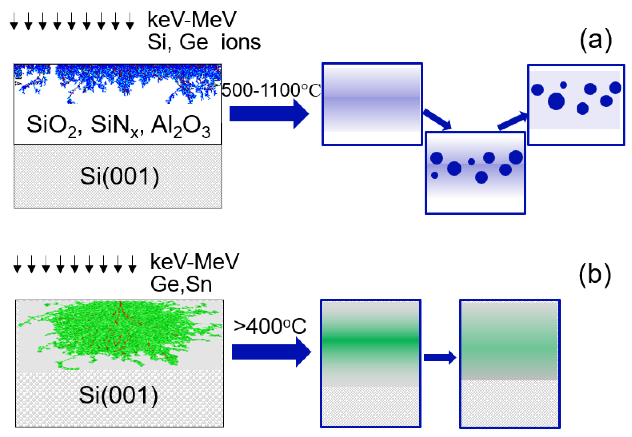
Several experimental methods have been used in the past to fabricate Si and Ge nanostructures [10]. If we focus on structures with dimensions comparable to the Bohr radius and the 3-dimensional (3D) confinement case (quantum dots), several solid-state methods are available, including plasma-enhanced chemical vapor deposition (PECVD) [11], co-sputtering [18], molecular beam epitaxy (MBE) [19], ion implantation [20,21], and porous silicon [4]. Ion implantation is a complex process in which the ion beam modifies the properties of the implanted material, causing defect production and, potentially, phase transformation. The general fabrication steps are illustrated in Figure 1a. QD formation is achieved by implantation of Si, Ge, or any other elements that can precipitate into semiconducting QDs in the dielectric (SiO2, SiNx, or Al2O3) or in wide-band semiconductors with a larger band gap energy, making quantum confinement possible.
In order to achieve precipitation of Si or Ge quantum dots, over-stoichiometric concentrations have to be in the range of 1021–1022 atoms/cm3, equivalent to an ion dose of the order of 1016 atoms/cm2. In the implanted layers with a high density of Si, Si QDs will nucleate until the Si concentration in the host material is too low. After implantation, the formation of QDs is facilitated by annealing of the substrate, providing thermal energy to the implanted ions for diffusion. For longer annealing times, this process can be described as Oswald ripening. Notably, defects in the Si QD nucleation zone facilitate QD formation via a transient diffusion mechanism [22]. From the implantation energy and ion dose, the implanted ion concentration and depth profiles can be predicted (calculated) using Monte-Carlo programs, such as SRIM [23] or TRIDYN [24].
Unlike the indirect band gap Si and Ge, direct band gap alloys such as Si1−xGex or S1−x−yGexSny provide a promising path toward Si-compatible devices for light detection. The transition to a direct band gap is obtained for Ge content x > 0.25, and for Sn content y > 1.3x + 0.107. Adding Si to the alloy increases the critical concentration of Sn needed to reach a direct band gap. Si1−xGex or S1−x−y GexSny systems are an interesting example where the bandgap depends on both the composition of alloys and the strain. The type of band gap and its energy depends on the composition of the alloys. The binary alloy Ge1−ySny becomes a direct bandgap semiconductor with the bandgap energy of Eg = 0.5 eV at y = 0.11. However, adding Si to this system increases the critical Sn concentration required to reach a direct band gap. Subjecting the alloy to tensile strain reduces this concentration and changes the band gap energy. There has been progress in group IV photodetectors, however there is still room for improvement. For instance, in order to extend the wavelength cut-off, the concentration of Sn in the active layer has to be increased to 10–15%. One of the main challenges is the difficulty to obtain high-quality crystalline layers due to the low solubility of Sn in Ge (<1 at.%) and in Si (<0.1 at.%), both significantly below the critical content for the direct bandgap transition (10 at.%). CVD and MBE processes were explored recently, however alternative growth protocols are still needed to obtain higher Sn content materials and to improve the crystallinity quality and device performance. Ion implantation offers such a possibility, with the general fabrication steps shown in Figure 1b. However there have been only a few demonstrations of short-wave infrared range (SWIR) detectors fabricated in this way [25], and the results presented here provide a foundation for future improved devices.
The following Section focuses on details of the fabrication and characterization of Si-photonics light emitters and detectors, and discusses their challenges.
3. Results and Discussion
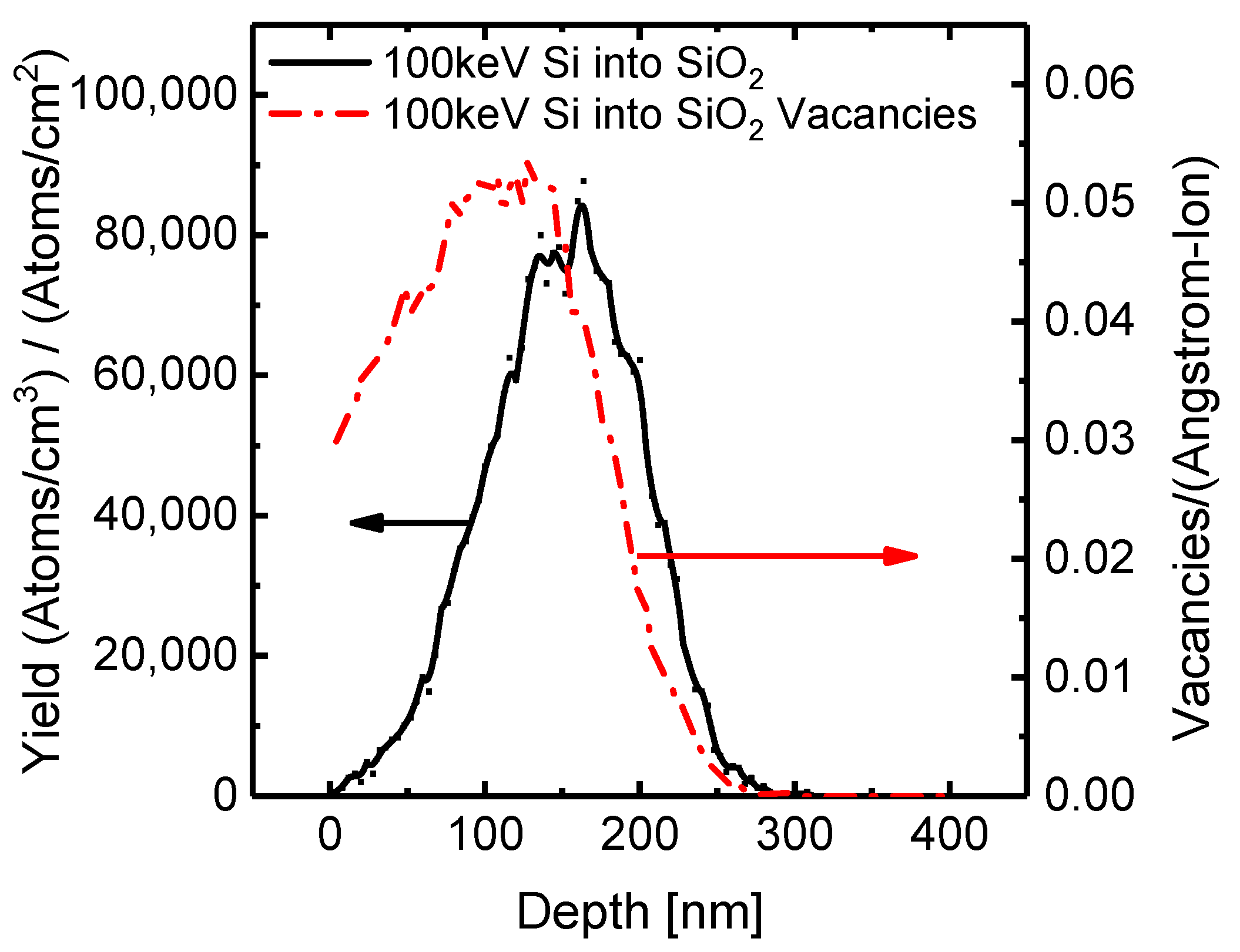
Emission wavelengths, both in the visible and short wavelength infrared, and lifetimes for light-emitting materials produced by ion implantation are summarized in Table 1. In the case of Si and Ge QDs, ion implantation produces a supersaturation of Si or Ge in a matrix material (often SiO2). On the other hand, ion implantation is characterized by the production of a large number of oxygen vacancies in the matrix. Figure 2 compares Si and oxygen vacancy depth profiles for 100 keV Si implants into SiO2. All defect types (point, line, planar, and volume) can be observed, therefore Figure 2 is a semiqualitative representation of the defect profile. The ion implantation process causes sputtering along with swelling of the substrate material, with a net effect of ~1 nm per 1 × 10¹⁶ atoms/cm2, in the 20–100 keV energy range [10]. Notably, the concentration of vacancies near the surface influences the formation of the Si QDs [17,22].
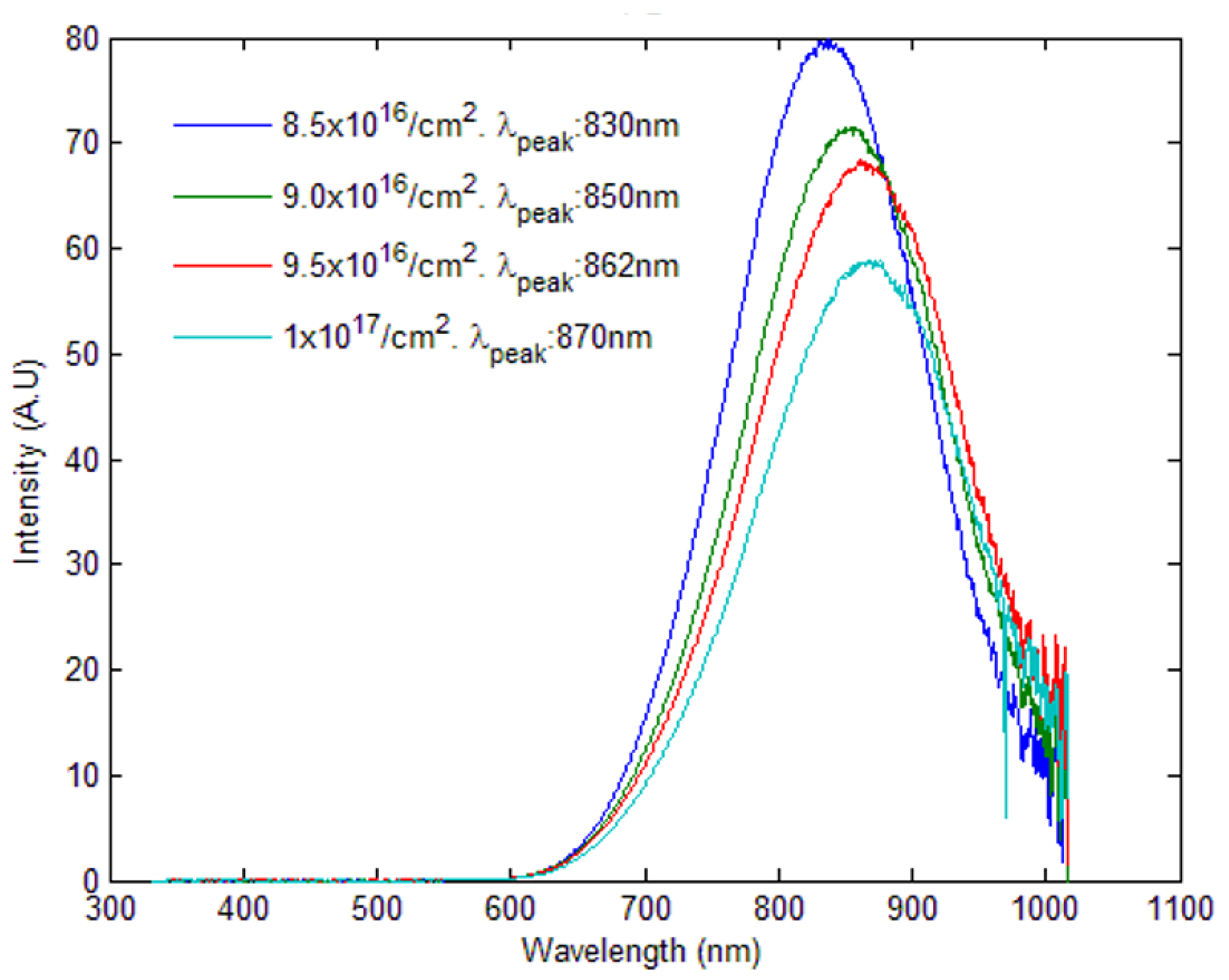
The Si QD diameter can be controlled by changing the Si implantation dose, as presented in Figure 3. Photoluminescence (PL) measurements were performed at room temperature with a 325 nm laser at 17 mW, an effective power density of 0.64 W/cm2, and were analyzed by an Ocean Optics spectrometer. From the position of the PL maximum for the 1 × 10¹⁷ Si/cm2 sample at 870 nm (1.42 eV), we can estimate an average Si QD diameter of D = 2.07 nm, using bandgap energy of Eg (D) = Eg (∞) + , where Eg(∞) = 1.1 eV for crystalline Si, and A = 1.39.
Lower Si implantation doses (in the high 1016 atoms/cm2 range) result in smaller QD diameters, for the same annealing conditions, and therefore in smaller wavelengths of emission (larger band gap) [32].
Ge QDs are promising materials for Si photonics [10]. As the Ge bandgap is 0.66 eV (equivalent to the wavelength of λ = 1876 nm), Ge QDs offer the possibility to achieve light emission in SWIR. However, producing efficient light emitting Ge QDs has been a challenge. Photoluminescence from Ge QDs in SiO2 has been attributed to oxygen-related defects at the Ge QDs/SiO2 interface, in addition to emissions from Ge QDs themselves producing light in the visible range or at SWIR range (Table 1) [19,21,27,28]. As a result of the significant dispersion of bandgap energy for Ge with a QD diameter, one can predict PL emission anywhere between λ = 961 nm for a medium confinement model (A = 2.69), which is more characteristic for crystalline dots, to PL at λ = 497 nm for a strong confinement model, for amorphous Ge QDs (A = 7.88), using the equation Eg (D) = 0.66 eV + [20]. Therefore, there remains much fundamental research to be done.
To qualify as a host material, the band gap of the material must be large enough for quantum confinement, while at the same time having a permittivity that allows for a refractive index variation for photonic circuits. Al2O3 satisfies these criteria, and has the advantage of being optically transparent, which could facilitate transparent devices [33]. The publication record for Si-QDs in Al2O3 is sparse, because researchers have found difficulty in producing Si-QDs in this material [30,33,34]. In the cases in which Si-QD formation has been reported, the luminescence from these Si-QD has been either very low in intensity, or absent. Researchers have proposed various reasons for the lack of PL due to Si-QD. For example, Kovalev et al [33]. researched the optical and structural properties of Si-QDs in crystalline and amorphous Al2O3, and concluded that Si-QDs did not form in crystalline Al2O3 films, but did form in amorphous Al2O3 films. Kovalev et al. [33] reported that only oxygen defect-related photoluminescence (PL) peaks were observed. Similar PL results were reported by Yerci et al. [35], who argued that the lack of PL from Si-QDs was due to mechanical stress on the Si-QDs at their interface with the surrounding matrix, caused by lattice mismatch. Si QDs form at relatively high temperatures (800–1200 °C). The large mismatch in thermal expansion coefficients between Al2O3 and Si (αL = 5.3 × 10⁻⁶ K−1 for sapphire, αL = 2.56 × 10⁻⁶ K−1 for Si) implies that during cooling, Si QDs shrink less than the surrounding matrix, resulting in compressive stress. Integration into device structures will require a better understanding of optical properties, as well as the composition of the Si quantum structures/dielectric matrix interface.
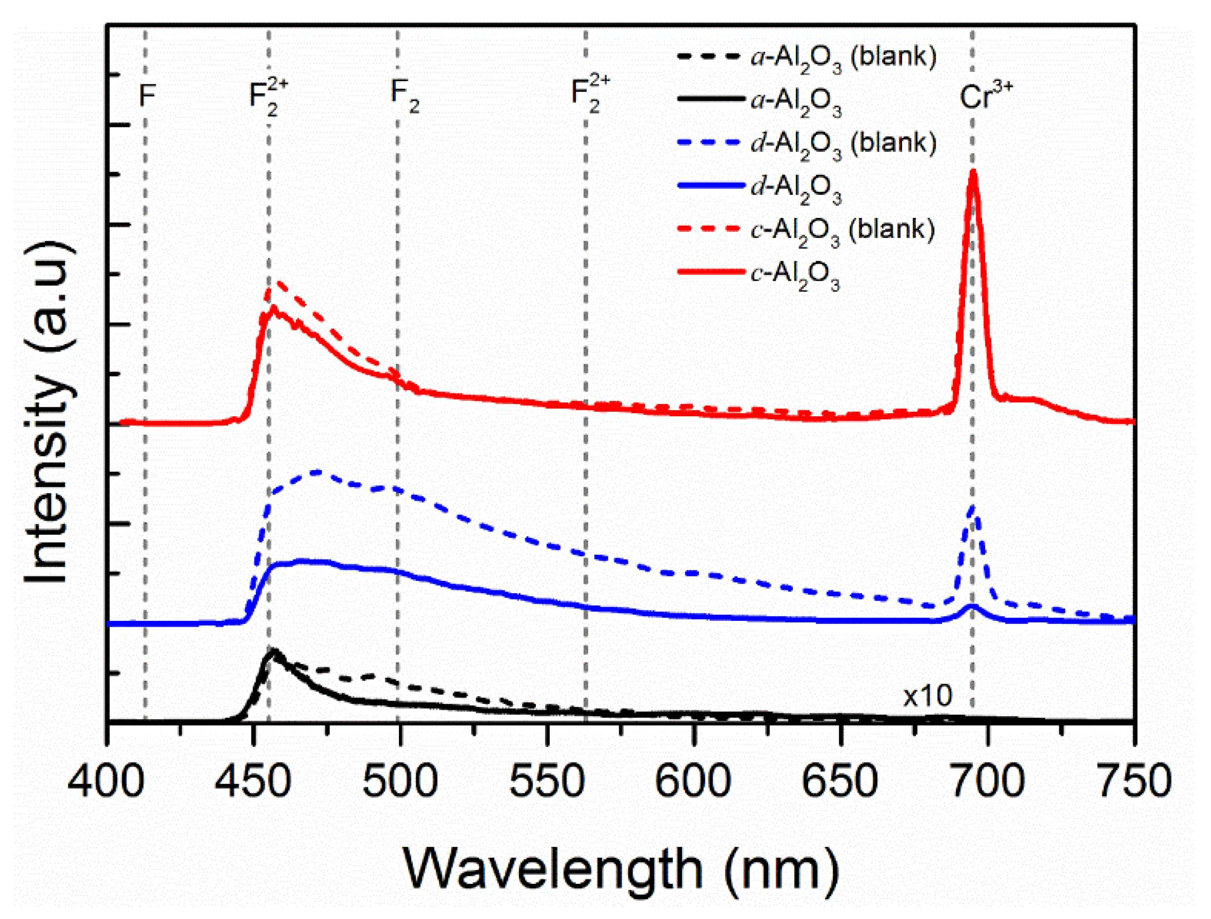
Defects in the matrix can strongly impact the growth of Si-QDs by solid state precipitation, by controlling the Si diffusion. To explore the effects of matrix crystallinity on the formation of Si QDs in Al2O3 and the resulting optical properties (luminescence), we studied anodized amorphous Al2O3 (a-Al2O3), crystalline (c-Al2O3) and disordered Al2O3 (d-Al2O3) produced by implanting O ions into crystalline α-Al2O3. All samples (a-Al2O3, d-Al2O3, and c-Al2O3) were implanted with Si ions at an incident angle of 7°, an energy of 90 keV, and a dose of 8 × 10¹⁶ ions/cm2, and were annealed at 1300 K in N2 gas for 1 h.
Figure 4 shows the PL spectra from virgin and Si-implanted Al2O3, comparing crystalline, disordered, and amorphous, and illustrating the significant impact of the matrix crystallinity. The main defects (or color centers) that formed in Al2O3 were those caused by oxygen vacancies and divacancies, which were F (O vacancies with two electrons, 413 nm), F+ (O vacancies with one electron, 326 nm), F2 (O divacancies with four electrons, 516 nm), F2+ (O divacancies with three electrons, 380 nm), and F22+ (O divacancies with two electrons, 563 nm) centers [36]. These oxygen defects can be found in the intrinsic Al2O3 film or can be introduced by bombarding the film with high-energy particles (such as neutrons, electrons, or ions) [34,37]. Crystalline Al2O3 will also frequently have Cr3+ and Ti3+ impurities, substituting Al, or taking cationic vacancy sites. These defects have luminescence peaks, with their characteristics summarized in Table 1. We observed that all samples showed a peak that begins at the short-wavelength detection limit (450 nm) and had a tail that extended up to 600 nm. The intensity of the peaks in both regions decreased after Si implantation and annealing [38]. The PL spectra for the d-Al2O3 and c-Al2O3 samples exhibited a sharp peak at 694 nm with a full width half maximum (FWHM) around 5 nm. This peak was due to the optical transition between d orbitals (d → d) of Cr3+ impurities with a d3 electronic configuration.
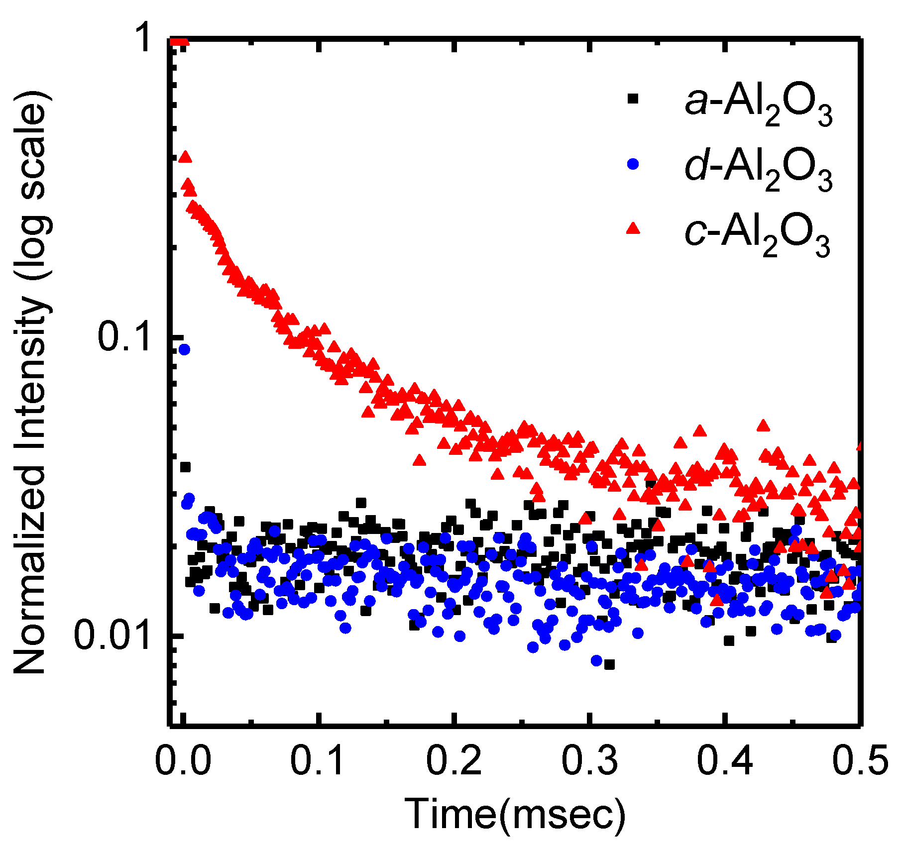
Figure 5 shows time-resolved photoluminescence (TRPL) curves from the same samples. The 405 nm laser diode was pulsed using a 3310 A HP function generator, and the time resolution of our setup was 100 ns. Decay curves were acquired using a R7400U-20 Hamamatsu photomultiplier tube (PMT) with a spectral range of 300–900 nm and peak sensitivity of 630 nm. It is found that samples a-Al2O3 and d-Al2O3 exhibited only short lifetimes, i.e., shorter than the time resolution of our system ~125 ns. Overall, the long lifetime (~3 ms) observed in TRPL from the sample c-Al2O3 may be attributable to Cr3+, for which other researchers have reported a PL lifetime between 3–4.3 ms [39]. The fast lifetime observed for samples a-Al2O3 and d-Al2O3 was likely caused by F+ center defects, which exhibited PL lifetimes shorter than 70 ns [37]. A detailed analysis of the TRPL data will be reported [38]. Note the luminescence due to Cr3+ and F centers in Al2O3 may have applications in which control of the luminescence lifetime is useful, as it can be manipulated by varying the contribution of fast (F) and slow (Cr3+) components. The latter phenomenon can be applied, for instance, in the area of radiation dosimetry.
Table 1 summarizes photoluminescence characteristics from Er-implanted Si and SiO2, as well as comparison to other rare-earth emitters, demonstrating its potential as a light source in the technologically important 1500 nm wavelength range. PL results reported by Franzo et al. [31] show that the Er peak at 1.54 μm is two orders of magnitude larger in samples containing Si QDs compared to pure SiO2. Si QDs were fabricated by implanting 80 keV Si ions (1 × 10¹⁷ atoms/cm2) in a 300 nm SiO2/Si (001) film, where (001) is the Miller index of the Si wafer, followed by an 1100 °C annealing fo, 1 h in dry N2. Er (with doses in the ~2 × 10¹³–4 × 10¹⁴ atoms/cm2 range) was implanted at 300 keV with the Er peak located at the same depth as the Si QDs. The intensity of the PL peak due to the rare earth element was also strongly dependent on the wavelength of the excitation laser, and inversely correlated with the luminescence due to Si QDs. The authors argued that excitons can either recombine with the Si QDs emission or give their energy to the Er 4f shell. This system presented a demonstration of energy transfer from the excitons confined in the Si QDs to the Er ions.
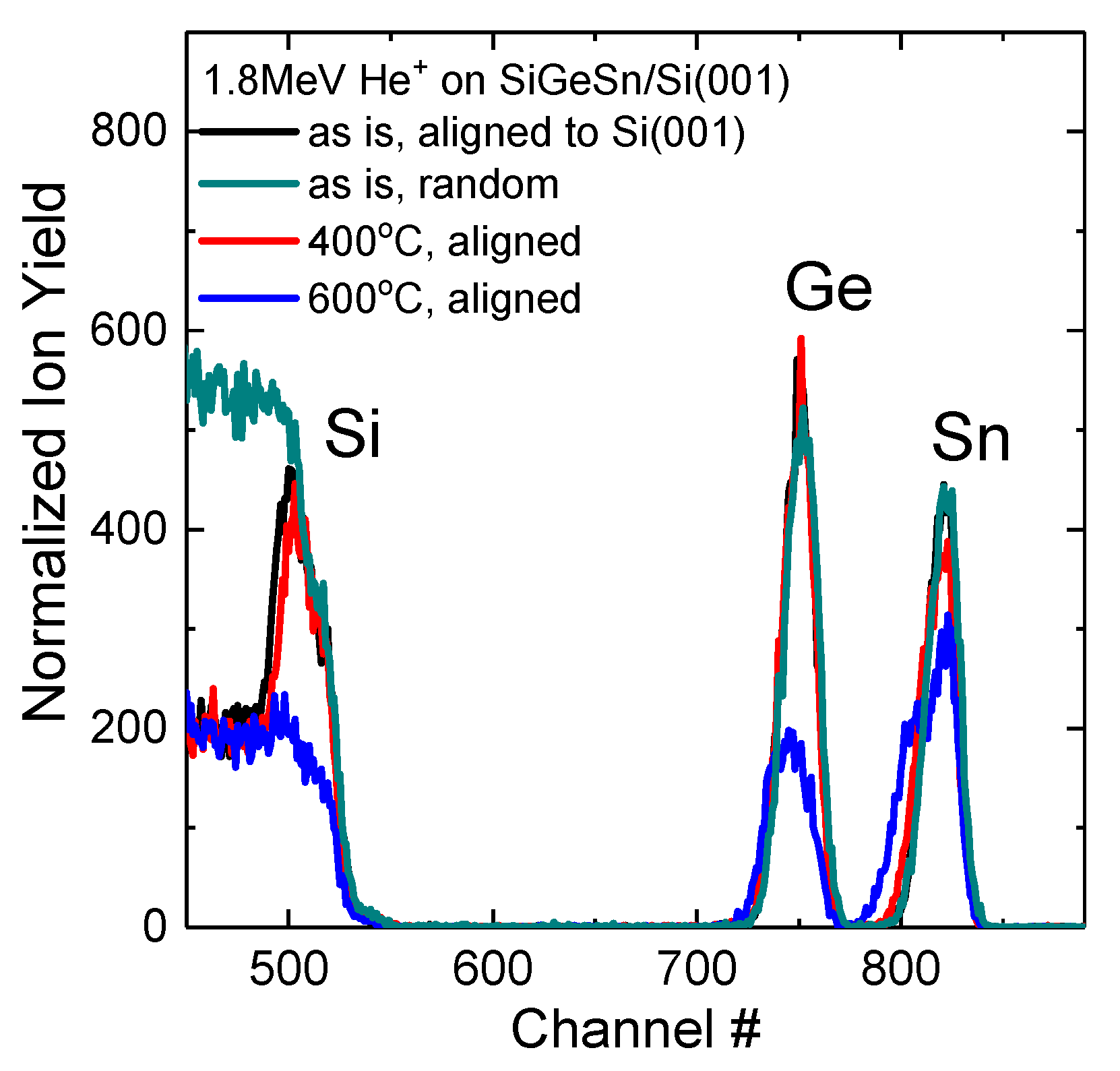
A preliminary study of SiGeSn alloys for detector applications. Si1−x−yGexSny alloys (with x = 0–0.2; y = 0–0.08) was performed for operation at wavelengths of 1.2–1.5 µm were fabricated by ion implantation with Ge and Sn at 65 keV and 100 keV, respectively, at an implantation angle of 7°. SRIM calculations gave us a projected range of 50 ± 20 nm for both Ge and Sn with these implantation parameters. The Ge fluence ranged from 2.5 × 10¹⁶ Ge/cm2 to 1.0 × 10¹⁷ Ge/cm2, while the Sn fluence ranged from 1.0 × 10¹⁶ to 4.0 × 10¹⁶ Sn/cm2. Thermal annealing was performed in a furnace (in dry N2) at 400–800 °C to ensure proper crystallization. Rutherford backscattering spectroscopy (RBS) spectra were obtained from the Si1−x−yGexSny samples before and after annealing, using 1.8 MeV He+ with a Si detector at 170° in the Cornell geometry, and are presented in Figure 6. There is no indication of Ge or Sn loss during these high-temperature anneals, and channeling spectra suggest that annealing temperatures ≥600 °C are sufficient to repair most of the damage caused by Ge and Sn implantation, consistent with previous studies for SiGe heterostructures.
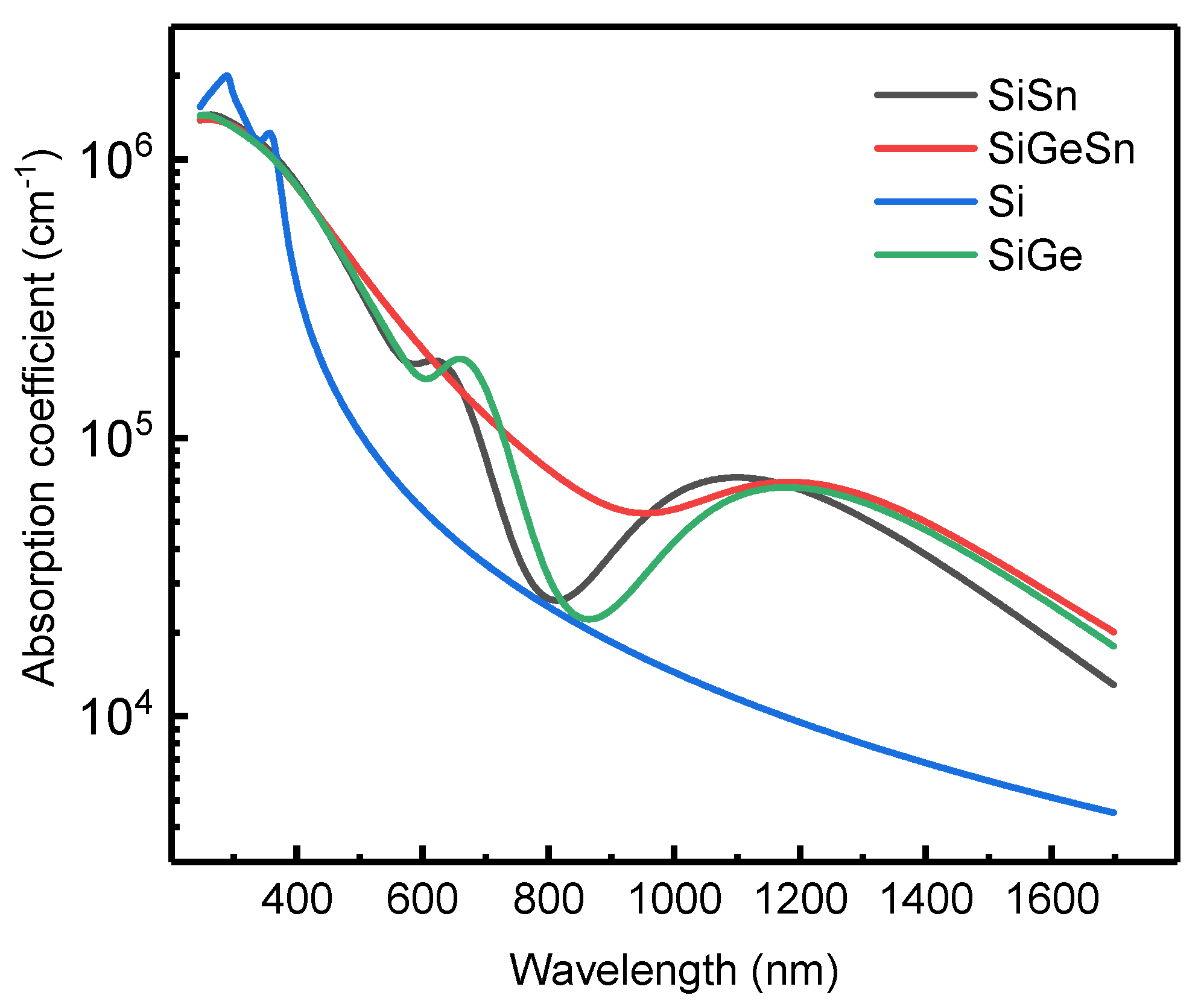
Optical spectroscopic ellipsometry was carried out using a Woollam M2000V model instrument, with a laser spot diameter of 1–3 mm at angles between 45° and 85°. Figure 7 shows the calculated absorption coefficient as a function of wavelength for Si0.72Ge0.2Sn0.08, Si0.92Sn0.08, and Si0.8Ge0.2 samples, with Si (001) as a reference [16]. For all of the samples, there is a significant increase in absorption for wavelengths of 400 nm and above. If we focus on absorption at 1500 nm (close to commercially important 1550 nm wavelength), absorption coefficients of 28,000 ± 50 cm−1, 33,000 ± 50 cm−1, and 33,100 ± 50 cm−1 were measured for Si0.92Sn0.08, Si0.8Ge0.2, and Si0.72Ge0.2Sn0.08, respectively. All three values were at least an order of magnitude higher compared to the pure Si measured in our experimental setup.
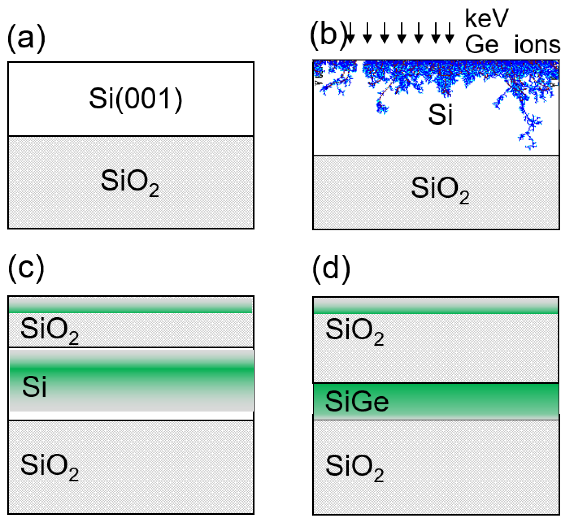
Ge is considered as a promising material for Si photon detectors due to the possibility of direct epitaxy on Si and the high adsorption coefficient in the SWIR, as mentioned before. However, during MBE growth, relatively thick SixGe1−x buffer layers are required to transition from Si to Ge during the growth. An elegant method for the formation of high-Ge content SixGe1−x on Silicon-on-Insulator (SOI) was reported by Anthony et al., using a Ge condensation technique [15]. In this method, low-Ge content SiGe was produced by implantation on SOI and then thermally oxidized. The general fabrication scheme is presented in Figure 8. Fabrication starts with 33 keV 5.0 × 10¹⁶ Sn/cm2 Ge+ ion implantation into an SOI substrate (Figure 8a,b). After implantation, the samples were annealed in a tube furnace at 900–1080 °C in a humid O2 atmosphere. Under these conditions, Si oxidizes preferentially, over the Ge, resulting in the growth of additional SiO2 and the segregation of a thin layer of high-Ge content SiGe, with peak Ge concentrations between 43 and 95% (Figure 8c,d) [15]. This implantation/condensation approach does not require epitaxial growth of SiGe, and provides a method for selective inclusion of SiGe materials with a high Ge content into a Si-photonics detector fabrication process.
4. Conclusions
Ion beam modification methods are valuable tools to fabricate novel materials for Si photonic platforms. Here, we reviewed several novel materials fabricated by ion implantation for light emitters and detectors. Si quantum dots (QDs) can be formed in SiO2, Si3Nx, and Al2O3 matrices by ion implantation, followed by high temperature annealing. We showed that the process of Si QD formation is strongly dependent on the matrix crystallinity and defects. The formation of Si quantum dots in a disordered matrix can be enhanced by transient enhanced diffusion. There are cases in which luminescent lifetimes are dominated by bright emitting defects that can be explored for future optoelectronic devices. There have been a limited number of studies demonstrating SiGe and SiGeSn alloys produced by ion implantation, however the first results are encouraging. In the second case study, SiGeSn alloys were produced by ion implantation, showing high absorption coefficients and low light penetration depths in the SWIR range, which can be explored as a route for Si photonics detectors in the future.
Author Contributions
L.V.G. and P.J.S. significantly contributed to the conceptualization and writing of the paper. All authors have read and agreed to the published version of the manuscript.
Funding
The Applied Nuclear Physics Conference 2021, where this work was presented, was funded
by the European Physics Society, MDPI, and National Electrostatic Cor-poration. We thank Natural
Science and Engineering Research Council of Canada (NSERC) for financial support.
Data Availability Statement
Not applicable.
Conflicts of Interest
The authors declare no conflict of interest.
References
- Ye, W.N.; Xiong, Y.L. Review of silicon photonics: History and recent advances. J. Mod. Opt. 2013, 60, 1299–1320. [Google Scholar] [CrossRef]
- Ion Implantation: Synthesis, Applications and Technology; Pogrebnjak, A.D. (Ed.) Nova Science Publishers: Hauppauge, NY, USA, 2019; p. 334. [Google Scholar]
- Zhou, Z.; Yin, B.; Michel, J. On-chip light sources for silicon photonics. Light Sci. Appl. 2015, 4, e358. [Google Scholar] [CrossRef]
- Cullis, A.; Canham, L.T.; Calcott, P. The structural and luminescence properties of porous silicon. J. Appl. Phys. 1997, 82, 909–965. [Google Scholar] [CrossRef]
- Fauchet, P.; Ruan, J.; Chen, H.; Pavesi, L.; Dal Negro, L.; Cazzaneli, M.; Elliman, R.; Smith, N.; Samoc, M.; Luther-Davies, B. Optical gain in different silicon nanocrystal systems. Opt. Mater. 2005, 27, 745–749. [Google Scholar] [CrossRef]
- Rong, H.; Liu, A.; Jones, R.; Cohen, O.; Hak, D.; Nicolaescu, R.; Fang, A.; Paniccia, M. An all-silicon Raman laser. Nature 2005, 433, 292–294. [Google Scholar] [CrossRef] [PubMed]
- Kenyon, A. Erbium in silicon. Semicond. Sci. Technol. 2005, 20, R65. [Google Scholar] [CrossRef]
- Liu, J.; Sun, X.; Pan, D.; Wang, X.; Kimerling, L.C.; Koch, T.L.; Michel, J. Tensile-strained, n-type Ge as a gain medium for monolithic laser integration on Si. Opt. Express 2007, 15, 11272–11277. [Google Scholar] [CrossRef]
- Sun, X.; Zadok, A.; Shearn, M.J.; Diest, K.A.; Ghaffari, A.; Atwater, H.A.; Scherer, A.; Yariv, A. Electrically pumped hybrid evanescent Si/InGaAsP lasers. Opt. Lett. 2009, 34, 1345–1347. [Google Scholar] [CrossRef] [Green Version]
- Barbagiovanni, E.G.; Lockwood, D.J.; Simpson, P.J.; Goncharova, L.V. Quantum confinement in Si and Ge nanostructures: Theory and experiment. Appl. Phys. Rev. 2014, 1, 47. [Google Scholar] [CrossRef] [Green Version]
- Cadogan, C.C.; Goncharova, L.V.; Simpson, P.J.; Nguyen, P.H.; Wang, Z.Q.; Sham, T.K. Influence of hydrogen passivation on the luminescence of Si quantum dots embedded in Si3Nx. J. Vac. Sci. Technol. B 2016, 34, 061202. [Google Scholar] [CrossRef]
- Kenyon, A.; Trwoga, P.; Pitt, C.; Rehm, G. The origin of photoluminescence from thin films of silicon-rich silica. J. Appl. Phys. 1996, 79, 9291–9300. [Google Scholar] [CrossRef]
- Thomson, D.; Zilkie, A.; Bowers, J.E.; Komljenovic, T.; Reed, G.T.; Vivien, L.; Marris-Morini, D.; Cassan, E.; Virot, L.; Fédéli, J.-M. Roadmap on silicon photonics. J. Opt. 2016, 18, 073003. [Google Scholar] [CrossRef]
- Ackert, J.J.; Thomson, D.J.; Shen, L.; Peacock, A.C.; Jessop, P.E.; Reed, G.T.; Mashanovich, G.Z.; Knights, A.P. High-speed detection at two micrometres with monolithic silicon photodiodes. Nat. Photon. 2015, 9, 393–396. [Google Scholar] [CrossRef]
- Anthony, R.; Haddara, Y.; Crowe, I.; Knights, A. SiGe-on-insulator fabricated via germanium condensation following high-fluence Ge+ ion implantation. J. Appl. Phys. 2017, 122, 065306. [Google Scholar] [CrossRef] [Green Version]
- Western University, London, ON, Canada. Growth and optical properties of SiGeSn alloys produced by ion implantation. Western University, London, ON, Canada. 2022; In preparation. [Google Scholar]
- Hellborg, R.; Whitlow, H.; Zhang, Y. Ion Beams in Nanoscience and Technology; Springer: Berlin/Heidelberg, Germany, 2010. [Google Scholar] [CrossRef]
- Pi, X.; Zalloum, O.; Knights, A.; Mascher, P.; Simpson, P. Electrical conduction of silicon oxide containing silicon quantum dots. J. Phys. Condens. Matter 2006, 18, 9943. [Google Scholar] [CrossRef] [Green Version]
- Lockwood, D.J.; Rowell, N.L.; Barbagiovanni, E.G.; Goncharova, L.V.; Simpson, P.J.; Berbezier, I.; Amiard, G.; Favre, L.; Ronda, A.; Faustini, M.; et al. Photoluminescence Efficiency of Germanium Dots Self-Assembled on Oxides. ECS Trans. 2013, 53, 185–206. [Google Scholar] [CrossRef]
- Barbagiovanni, E.G.; Lockwood, D.J.; Simpson, P.J.; Goncharova, L.V. Quantum confinement in Si and Ge nanostructures. J. Appl. Phys. 2012, 111, 034307. [Google Scholar] [CrossRef] [Green Version]
- Kanemitsu, Y.; Masuda, K.; Yamamoto, M.; Kajiyama, K.; Kushida, T. Near-infrared photoluminescence from Ge nanocrystals in SiO2 matrices. J. Lumines. 2000, 87, 457–459. [Google Scholar] [CrossRef]
- Mokry, C.R.; Simpson, P.J.; Knights, A.P. Role of vacancy-type defects in the formation of silicon nanocrystals. J. Appl. Phys. 2009, 105, 114301. [Google Scholar] [CrossRef]
- Ziegler, J.F.; Biersack, J.P. SRIM-The Stopping and Range of Ions in Matter; SRIM Company: Onondaga, NY, USA, 2008. [Google Scholar]
- Müller, T.; Heinig, K.-H.; Möller, W. Size and location control of Si nanocrystals at ion beam synthesis in thin SiO2 films. Appl. Phys. Lett. 2002, 81, 3049–3051. [Google Scholar] [CrossRef] [Green Version]
- Anthony, R.; Hagan, D.E.; Genuth-Okon, D.; Maestro, L.M.; Crowe, I.F.; Halsall, M.P.; Knights, A.P. Extended wavelength responsivity of a germanium photodetector integrated with a silicon waveguide exploiting the indirect transition. IEEE J. Sel. Top. Quantum Electron. 2019, 26, 1–7. [Google Scholar] [CrossRef]
- Jayatilleka, H.; Diamare, D.; Wojdak, M.; Kenyon, A.J.; Mokry, C.R.; Simpson, P.J.; Knights, A.P.; Crowe, I.; Halsall, M.P. Probing energy transfer in an ensemble of silicon nanocrystals. J. Appl. Phys. 2011, 110, 033522. [Google Scholar] [CrossRef]
- Maeda, Y.; Tsukamoto, N.; Yazawa, Y.; Kanemitsu, Y.; Masumoto, Y. Visible photoluminescence of Ge microcrystals embedded in SiO2 glassy matrices. Appl. Phys. Lett. 1991, 59, 3168–3170. [Google Scholar] [CrossRef] [Green Version]
- Lopes, J.M.J.; Zawislak, F.C.; Behar, M.; Fichtner, P.F.P.; Rebohle, L.; Skorupa, W. Cluster coarsening and luminescence emission intensity of Ge nanoclusters in SiO2 layers. J. Appl. Phys. 2003, 94, 6059–6064. [Google Scholar] [CrossRef] [Green Version]
- Yanagiya, S.; Ishida, M. Optical and electrical properties of Al2O3 films containing silicon nanocrystals. J. Electron. Mater. 1999, 28, 496–502. [Google Scholar] [CrossRef]
- Yin, S.; Xie, E.Q.; Zhang, C.H.; Wang, Z.G.; Zhou, L.H.; Ma, Y.Z.; Yao, C.F.; Zang, H.; Liu, C.B.; Sheng, Y.B. Photoluminescence character of Xe ion irradiated sapphire. Nucl. Instrum. Methods Phys. Res. Sect. B Beam Interact. Mater. At. 2008, 266, 2998–3001. [Google Scholar] [CrossRef]
- Franzò, G.; Iacona, F.; Vinciguerra, V.; Priolo, F. Enhanced rare earth luminescence in silicon nanocrystals. Mat. Sci. Eng. B 2000, 69, 335–339. [Google Scholar] [CrossRef]
- Barbagiovanni, E.G. Influence of Quantum Dot Strucutre on the Optical Properteis of Group IV Materials Fabricated by Ion Implantation. Ph.D Thesis, The University of Western Ontario, London, ON, Canada, 2012. Available online: https://ir.lib.uwo.ca/cgi/viewcontent.cgi?article=1999&context=etd (accessed on 20 January 2022).
- Kovalev, A.; Wainstein, D.; Tetelbaum, D.; Mikhaylov, A.; Pavesi, L.; Ershov, A.; Belov, A. The electron and crystalline structure features of ion-synthesized nanocomposite of Si nanocrystals in Al2O3 matrix revealed by electron spectroscopy. Proc. J. Phys. Conf. Ser. 2008, 100, 072012. [Google Scholar] [CrossRef] [Green Version]
- Evans, B.D.; Pogatshnik, G.J.; Chen, Y. Optical properties of lattice defects in α-Al2O3. Nucl. Instr. Meth. B Beam Interact. Mater. At. 1994, 91, 258–262. [Google Scholar] [CrossRef]
- Yerci, S.; Serincan, U.; Dogan, I.; Tokay, S.; Genisel, M.; Aydinli, A.; Turan, R. Formation of silicon nanocrystals in sapphire by ion implantation and the origin of visible photoluminescence. J. Appl. Phys. 2006, 100. [Google Scholar] [CrossRef] [Green Version]
- Itou, M.; Fujiwara, A.; Uchino, T. Reversible Photoinduced Interconversion of Color Centers in α-Al2O3 Prepared under Vacuum. J. Phys. Chem. C 2009, 113, 20949–20957. [Google Scholar] [CrossRef]
- Evans, B.D.; Stapelbroek, M. Optical properties of the F+ center in crystalline Al2O3. Phys. Rev. B 1978, 18, 7089. [Google Scholar] [CrossRef]
- Western University, London, ON, Canada. The influence of matrix crystallinity on the formation of Si-NPs in Al2O3. Western University, London, ON, Canada. 2022; In preparation. [Google Scholar]
- Aizawa, H.; Toba, E.; Katsumata, T.; Komuro, S.; Morikawa, T. Chromium doped phosphor based fiber-optic thermometer. In Proceedings of the Second IEEE International Conference On Sensors, Toronto, Otario, Canada, 22–24 October 2003; IEEE Xplore. pp. 88–91. [Google Scholar]
Figure 1.
Schematic diagram of ion implantation for the fabrication of (a) Si or Ge quantum dots (QDs) in SiO2 for light emission and (b) SiGe and SiGeSn layers for light absorption. (a) Supersaturated Si atoms nucleate into QDs when high-temperature processing is applied, and with time, Si atoms adsorb into neighboring QDs, following the transient diffusion mechanism [22]. (b) Implanted Ge and/or Sn atoms diffuse and form a crystalline lattice with Si.

Figure 2.
Implanted Si ion yield (black curve with values shown on the left Y-axis, indicated with black arrow) and vacancy profile (red dash-dotted line with values shown on the right axis, indicated by red arrow) as a function of depth in SiO2 for 100 keV incident energy, simulated with SRIM code [23].

Figure 3.
Photoluminescence spectra from Si quantum dots in SiO2/Si (001) produced by 90 keV Si+ ion implantation. Si implantation doses are shown [32]. The maximum wavelengths (λpeak, nm) of light emission are provided for each spectrum.
Figure 3.
Photoluminescence spectra from Si quantum dots in SiO2/Si (001) produced by 90 keV Si+ ion implantation. Si implantation doses are shown [32]. The maximum wavelengths (λpeak, nm) of light emission are provided for each spectrum.

Figure 4.
Photoluminescence spectra of α-Al2O3 (amorphous, solid black line), d-Al2O3 (disordered, solid blue line), and c-Al2O3 (crystalline, solid red line) samples implanted with Si ions and annealed at 1200 °C (with a vertical offset and magnified where indicated for clarity). The samples before implantation and annealing are labelled “blank”.

Figure 5.
Time-resolved photoluminescence curves for Si-implanted Al2O3. [38].
Figure 5.
Time-resolved photoluminescence curves for Si-implanted Al2O3. [38].

Figure 6.
Rutherford backscattering spectroscopy (RBS) spectra for 65 keV Ge- and 100 keV Sn-implanted Si (001) samples annealed at high temperatures. Here, (001) is the Miller index of the original Si wafer. Spectra measured in the aligned geometry are compared to random geometry results.
Figure 6.
Rutherford backscattering spectroscopy (RBS) spectra for 65 keV Ge- and 100 keV Sn-implanted Si (001) samples annealed at high temperatures. Here, (001) is the Miller index of the original Si wafer. Spectra measured in the aligned geometry are compared to random geometry results.

Figure 7.
Absorption coefficient of SiGe, SiSn, and SiGeSn alloys fabricated by ion beam implantation at the 200–1700 nm range compared to the referenced Si (001) sample, measured using spectroscopic ellipsometry.
Figure 7.
Absorption coefficient of SiGe, SiSn, and SiGeSn alloys fabricated by ion beam implantation at the 200–1700 nm range compared to the referenced Si (001) sample, measured using spectroscopic ellipsometry.

Figure 8.
Schematic description of the two-step oxidation process: (a) starting substrate consists of 220 nm thick Si on 2000 nm Berried-Oxide Silicon-on-Insulator (BOX SOI); (b) implantation of 5 × 10¹⁶ Ge cm−2 at 33 keV; (c) primary oxidation at 870 °C used to cap the Silicon-Germanium-on-Insulator (SiGeOI, resulting in a mixed oxide; and (d) secondary oxidation at either 900° or 1000 °C to form final SiGeOI structure. Adapted from [15].


Table 1.
Emission wavelengths and lifetimes for luminescent materials produced by ion implantation. NR stands for “not reported”. QDs stands for “quantum dots”.
Table 1.
Emission wavelengths and lifetimes for luminescent materials produced by ion implantation. NR stands for “not reported”. QDs stands for “quantum dots”.
| Material or Defect Center | Luminescence Maximum (in nm) | Lifetime | Reference |
|---|---|---|---|
| Si QDs | 780–880 | 20–225 μs | [26] |
| Ge QDs | ~568 | NR | [27] |
| Ge QDs | 1240–1378 | NR | [21] |
| Ge QDs | 291 and 387 | NR | [28] |
| Al2O3 F | 413 | 480 ms | [29] |
| Al2O3 F+ | 326 | <7 ns | [29] |
| Al2O3 F2 | 516 | 68 ms | [29] |
| Al2O3 Cr3+ | 694 | 3–4.3 ms | [30] |
| Er-Si QDs | 980, 1540 | 3.0 ms | [31] |
| Yb-Si QDs | 980 | NR | [31] |
| Nd-Si QDs | 920 | NR | [31] |
| Tm- Si QDs | 780, 1650 | NR | [31] |
Publisher’s Note: MDPI stays neutral with regard to jurisdictional claims in published maps and institutional affiliations. |
© 2022 by the authors. Licensee MDPI, Basel, Switzerland. This article is an open access article distributed under the terms and conditions of the Creative Commons Attribution (CC BY) license (https://creativecommons.org/licenses/by/4.0/).
Share and Cite
MDPI and ACS Style
Goncharova, L.V.; Simpson, P.J. Ion Beam Modification for Si Photonics. Physics 2022, 4, 383-393. https://0-doi-org.brum.beds.ac.uk/10.3390/physics4020025
AMA Style
Goncharova LV, Simpson PJ. Ion Beam Modification for Si Photonics. Physics. 2022; 4(2):383-393. https://0-doi-org.brum.beds.ac.uk/10.3390/physics4020025
Chicago/Turabian StyleGoncharova, Lyudmila V., and Peter J. Simpson. 2022. "Ion Beam Modification for Si Photonics" Physics 4, no. 2: 383-393. https://0-doi-org.brum.beds.ac.uk/10.3390/physics4020025