Ion Implantation into Nonconventional GaN Structures


1
DECN, Instituto Superior Técnico (IST), University of Lisbon, Campus Tecnológico e Nuclear, 2695-066 Bobadela LRS, Portugal
2
INESC MN, 1000-029 Lisbon, Portugal
3
IPFN, Instituto Superior Técnico (IST), University of Lisbon, 1049-001 Lisbon, Portugal
Physics 2022, 4(2), 548-564; https://0-doi-org.brum.beds.ac.uk/10.3390/physics4020036
Submission received: 14 November 2021
/
Revised: 21 April 2022
/
Accepted: 22 April 2022
/
Published: 16 May 2022
(This article belongs to the Special Issue Selected Papers from Applied Nuclear Physics Conference 2021)
Abstract
:Despite more than two decades of intensive research, ion implantation in group III nitrides is still not established as a routine technique for doping and device processing. The main challenges to overcome are the complex defect accumulation processes, as well as the high post-implant annealing temperatures necessary for efficient dopant activation. This review summarises the contents of a plenary talk, given at the Applied Nuclear Physics Conference, Prague, 2021, and focuses on recent results, obtained at Instituto Superior Técnico (Lisbon, Portugal), on ion implantation into non-conventional GaN structures, such as non-polar thin films and nanowires. Interestingly, the damage accumulation is strongly influenced by the surface orientation of the samples, as well as their dimensionality. In particular, basal stacking faults are the dominant implantation defects in c-plane GaN films, while dislocation loops predominate in a-plane samples. Ion implantation into GaN nanowires, on the other hand, causes a much smaller density of extended defects compared to thin films. Finally, recent breakthroughs concerning dopant activation are briefly reviewed, focussing on optical doping with europium and electrical doping with magnesium.
1. Introduction
Group III nitride semiconductors, namely, GaN, AlN, InN and their ternary and quaternary compounds, became famous beyond the research community due to their application in light-emitting diodes (LEDs) and laser diodes for lighting and data storage. Their fame culminated in the attribution of the Nobel Prize in Physics in 2014 to Isamu Akasaki, Hiroshi Amano and Shuji Nakamura for the development of the blue light-emitting diode (LED) in the 1990s [1]. Today, nitride LEDs are the base technology for highly efficient white solid-state lighting and advanced photonics applications [2]. Many of these new applications rely on non-conventional structures, such as those incorporating non-polar nitrides (i.e., with a- or m-plane surface instead of the conventional c-plane structures) or nanowires (NWs) [3,4,5]. In this context, non-polar devices avoid efficiency losses due to the quantum-confined Stark effect. The electrical fields induced in c-plane quantum wells due to the polar crystal structure, reduce the electron–hole overlap and, thus, the probability of radiative carrier recombination, in particular, for long-wavelength emissions in the green and red spectral regions [6]. The advantages of devices based on NWs include their high crystalline quality compared to heteroepitaxial layers since the 3-dimensional (3D) structures allow for efficient strain relaxation minimizing the number of dislocations, as well as improved light extraction [7].
Less known but equally promising is the potential of these wide bandgap semiconductors for the development of high-temperature, high-power and high-frequency electronic devices [8]. Thanks to their wide bandgap and high electron mobility, III-nitrides are expected to outperform silicon power devices in terms of breakdown voltage and on-resistance, respectively, opening the possibility of huge energy savings. Novel applications of GaN power devices range from the automotive sector to smart grids. High switching speeds enable technologies, such as LiDAR (light detection and ranging) and space communications. Nevertheless, new design and processing techniques need to be developed and optimised for GaN power electronics to become competitive on a large industrial scale.
To date, doping for commercial devices is carried out during the growth. However, for the insertion of devices in integrated circuits and a more versatile device design, selective-area doping techniques, such as ion implantation, are highly desirable. While ion implantation is a key technology in the silicon industry, it is far from being established for the processing of nitrides. This is mainly due to the difficulties in efficiently removing implantation damage during post-implant thermal annealing. In fact, the main drawback of the ion implantation technique is the large number of lattice defects that are formed when a material is bombarded with energetic and heavy ions. Thermal annealing is required to remove defects and activate the implanted dopants. Despite the difficulties in annealing GaN, many breakthroughs were reported quite recently by applying ion implantation for the processing of diodes, transistors and even laser structures [9,10,11,12,13]. In many of these applications, ion beams are used for implant isolation [10,11,14] and to form current apertures [12,13] (thus taking advantage of implantation defects to modify the materials’ properties), but much progress has also been made concerning p-type doping using magnesium implants [15,16,17]. Thanks to these advances, several device designs were realised, including ion implantation steps, both in lateral [9,17,18,19] and vertical devices [20,21,22], and metal–oxide–semiconductor field-effect transistors (MOSFET) were fabricated using an all ion implantation process [23,24]. Of particular interest are vertical devices, which allow for higher breakdown voltages and overall smaller structures, for example, in current aperture vertical electron transistors (CAVETs). The current blocking layer (CBL) is a key feature in these devices, providing a barrier to current flow in the vertical direction, leaving only a small aperture for vertical flow. Si implantation was used to define this aperture in a p-GaN CBL, which was either fabricated during growth or by Mg-implantation [20,21]. Current apertures defined using ion implantation were also applied successfully for the fabrication of vertical cavity surface-emitting lasers (VCSELs) [12]. Al implantation was used in this case to define the vertical current path, showing that implantation defects are sufficient to block the current in the implanted region. Implanting impurities, such as Fe, leading to deep levels further improves the isolating properties and temperature stability [10,14]. Indeed, implant isolation was used in several III-nitride devices, such as for edge termination in GaN Schottky diodes and GaN/Si p-n diodes, allowing for suppressing leakage along the side walls and increasing the breakdown voltage [25,26]. In several other reports, implant isolation was further used to reduce leakage via the substrate [27,28]. Interestingly, detailed carrier profiling suggests that ion implantation deactivates carriers far beyond the depth of the damaged region seen in transmission electron microscopy images or predicted using Monte Carlo simulations [29].
First reports on ion implantation in GaN date back to the 1970s [30]. However, intense research only started around the millennium change when high-quality GaN heteroepitaxial films became readily available. Early research on ion implantation focused on such c-plane GaN films and was described in several comprehensive reviews [31,32,33,34]. The main conclusions can be summarised as follows: Due to efficient dynamic annealing effects, point defects can already recombine during the implantation keeping implantation damage low. In fact, a complete loss of single-crystalline order is only observed for implantation at cryogenic temperatures and very high fluences [35] or due to chemical effects, e.g., for fluorine implantation [36]. Nevertheless, the high mobility of point defects, even at low temperature [37], also leads to their interaction with each other or with native defects and, consequently, to the formation of thermally very stable point defect clusters and extended defects, such as stacking faults and dislocation loops. Indeed, these are the dominant types of defects in ion-implanted GaN, as well as in AlN and AlGaN alloys [38,39,40,41,42]. Extended defects and defect clusters are difficult to remove during post-implant annealing and can act as traps for free charge carriers, hampering the proper operation of devices [16].
In the past decade, fundamental research on implantation effects in III-nitrides has shifted from simple c-plane GaN films to more complex structures, including films with different surface orientations, ternary compounds or nanostructures. This review summarises the contents of a plenary talk, given at the Applied Nuclear Physics Conference, Prague, Czech Republic, in 2021, and focuses on recent results, obtained at the Laboratory of Accelerators and Radiation Technologies (LATR) of Instituto Superior Técnico (Lisbon, Portugal) [43], on ion implantation into such nonconventional GaN structures. These include non-polar GaN films grown on the a- and m-plane (as compared to the conventional c-plane) of the wurtzite lattice [44], as well as nanostructures, such as nanowires [45]. Although a complete review would go beyond the scope of this paper, some of the most promising reports on dopant activation found in the literature are also highlighted. In particular, ultra-high temperature annealing efficiently activates optical rare earth dopants, as well as electrical dopants.
2. Materials and Methods
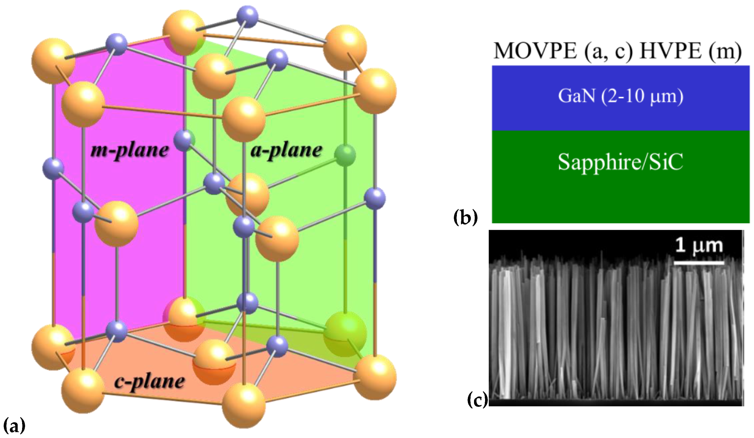
Figure 1a shows the thermodynamically most stable wurtzite crystal structure of GaN and the three major crystallographic planes, namely, (110), (0001) and (100), or the a-, c- and m-plane, respectively. For the present study, 3–10 μm thick GaN films were grown on sapphire or SiC substrates using metal–organic vapour-phase epitaxy (MOVPE) or hydride vapour phase epitaxy (HVPE) (Figure 1b). For the study, presented in Section 3.1, ion implantation of 300 keV Ar ions and in situ Rutherford backscattering spectrometry/channelling (RBS/C) analysis using 1.4 MeV He+ were performed at 15 K at the University of Jena, Germany [44].
NWs were grown using molecular beam epitaxy (MBE) on silicon substrates. Figure 1c shows a typical scanning electron microscopy (SEM) image of an as-grown sample. The NWs were grown vertically aligned along the c-axis and show m-plane side facets [46]. They had typical lengths of 2.5 μm and the width of the NWs was around 50–100 nm.
As an example of optical doping, NWs, as well as thin-film c-plane GaN, were implanted with 300 keV Eu ions (Section 3.2 and Section 3.3). Besides RBS/C, structural characterisation was performed using transmission electron microscopy (TEM), and X-ray diffraction (XRD) and optical activation of Eu3+ ions were studied using photoluminescence (PL) and nano-cathodoluminescence (CL).
3. Results and Discussion
In the following, some case studies on ion implantation in GaN are discussed. In Section 3.1, a detailed study of argon implantation in GaN thin films with different surface orientations illustrate the complex dynamics of defect accumulation in GaN due to efficient dynamic annealing effects [44]. Section 3.2 discusses ion implantation in GaN NWs [45]. Finally, Section 3.3 addresses doping via ion implantation and annealing. It focuses on optical doping via Eu-implantation, which has been an important research topic at LATR, Instituto Superior Técnico (Lisbon, Portugal), but recent advances found in the literature concerning electrical doping are also highlighted.
3.1. Implantation Damage Formation in a-, c- and m-Plane GaN
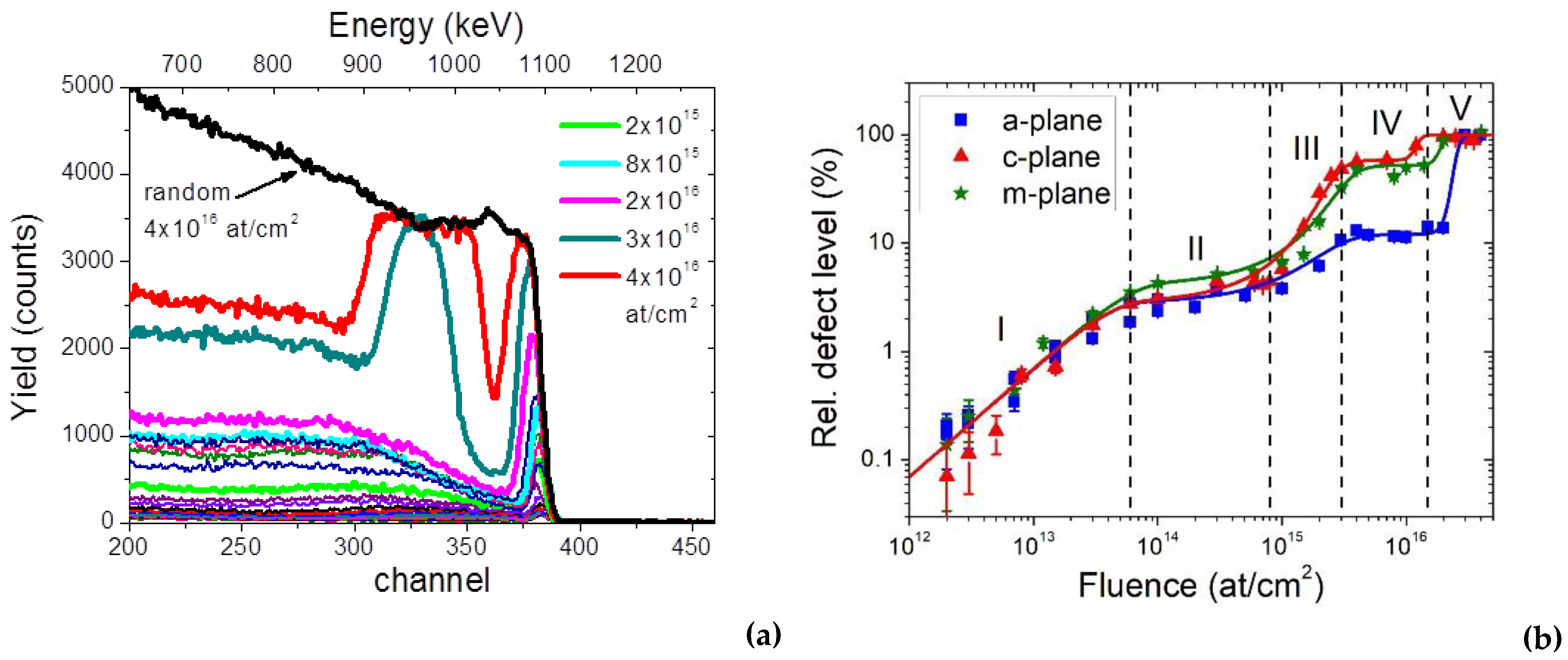
Typical RBS/C spectra for the a-plane GaN sample implanted using different Ar-fluences are shown in Figure 2a. The backscattering yield of the as-grown sample is very low. Minimum yields well below 2% were measured close to the surface for all three sample materials, evidencing excellent crystalline quality along the growth direction. As the fluence increases, the backscattering yield also increases, revealing the displacement of Ga-atoms from their lattice site. High dechannelling yields beyond the implanted region (below ~900 keV in Figure 2a) hint at the formation of extended defects [47] similar to what is observed for c-plane GaN [48]. After correction for this dechannelling yield, the fraction of displaced lattice atoms was extracted as a function of depth [44]. The maximum value of this relative defect level is plotted in Figure 2b as a function of the fluence for all three sample materials. Strong dynamic annealing effects are obvious from these damage build-up curves. Implantation damage does not increase linearly with the fluence but occurs in several regimes (marked in Figure 2b).
The curves are well fitted (lines in Figure 2b) using the defect accumulation and amorphisation model by Hecking [49]. According to this model, the linear increase of damage in regime I is due to defect formation in well-separated collision cascades. In regime II, the individual collision cascades start to overlap, leading to an increased recombination of vacancies and interstitials and an almost stable defect level. In regime III, the formation of extended defects and clusters leads to a strong increase in the defect level, which saturates again in regime IV. A full loss of the single crystalline order is observed in regime V for very high fluences above 1 × 10¹⁶ at/cm2. Similar curves were measured by several groups in c-plane GaN and AlGaN [38,50,51], nevertheless, it should be noted that, in some cases, chemical effects, as well as cascade density, can considerably change the defect accumulation in GaN [36,52,53].
Concerning the effect of different surface orientations, regimes I and II are similar for the three studied orientations and defect profiles agree well with ballistic models, such as Monte Carlo SRIM (stopping and ranges of ions in matter) [54] simulations [44]. For higher fluences (regimes III and IV), distinct behaviours are observed for the three samples with strikingly lower defect levels in a-plane GaN (note the logarithmic scale in Figure 2b). This effect was also confirmed for heavy ion gold and rare earth ion implantation [55,56]. In this regime, a large number of extended defects and clusters are formed. Two different scenarios could explain the surprising difference in the RBS/C results. On the one hand, it is possible that the same defects are formed but the efficiency with which they are detected depends on the chosen channelling directions. Thus, displaced atoms may be shadowed by the atomic rows along a certain direction and exposed to the analysing beam for channelling along another axis.
On the other hand, the low backscattering yield can reflect a real effect, i.e., the number of defects in a-plane GaN is considerably lower than in c- and m-plane GaN and/or different defect types are present.
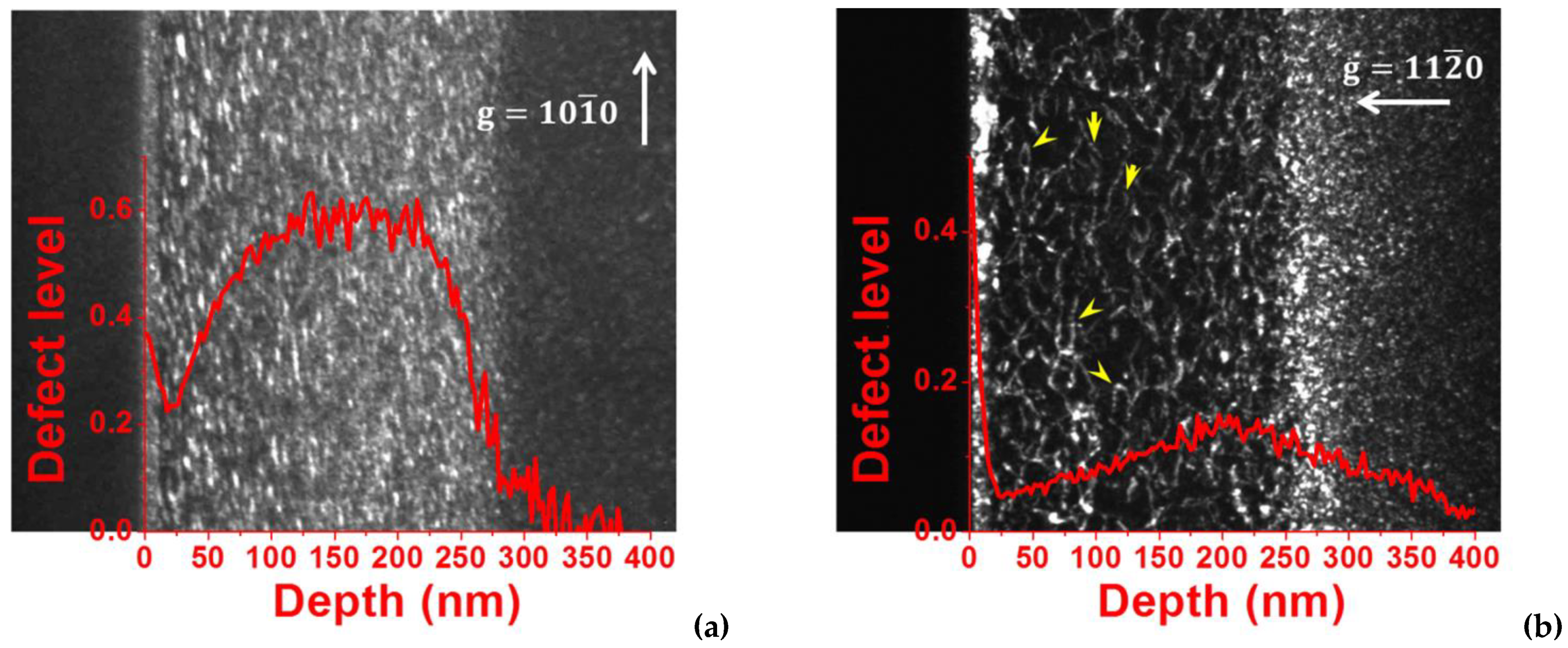
To differentiate between these two scenarios, TEM was performed on samples corresponding to regime IV, implanted using a fluence of 8 × 10¹⁵ at/cm2. Examples for TEM images of c- and a-plane samples are shown in Figure 3. They reveal that indeed the nature of extended defects is different in the two samples. While basal stacking faults, with the typical light contrast parallel to the surface (Figure 3a), are dominant in c-plane GaN, a-plane GaN shows a high concentration of dislocation loops with a [110] character (Figure 3b). The defect profiles derived from RBS/C were superimposed onto the TEM images and show a good agreement with the observed contrast for the m-plane sample. For the a-plane sample, pronounced surface damage was identified using both techniques. In deeper regions, TEM shows a layered structure with dislocation loops clearly observed until a depth of approximately 250 nm, while the region between 250 and 350 nm depth shows the typical contrast of defect clusters. This distinct defect morphology is not resolved in the RBS/C spectra. The extracted defect profile corresponds to atoms that are displaced from their lattice sites. These displaced atoms, mainly due to defect clusters, lead to direct backscattering of the alpha particles, while the distortion of the lattice by dislocation loops gives rise to a high dechannelling yield. In future work, it will be interesting to implement a model for these defects in a Monte Carlo code, which would allow for a more quantitative analysis of RBS/C spectra in the presence of different defect morphologies [57]. Nevertheless, the depth range at which defects are visible was the same for both techniques. It is worth mentioning that a similar layered structure was observed using TEM in ion-implanted c-plane GaN, where stacking faults were formed at the depth of nuclear energy deposition, while deeper regions were free of stacking faults but instead present defect clusters [58].
3.2. Ion Implantation in GaN Nanowires
In Section 3.1, the complex damage build-up processes, occurring in GaN thin films upon ion implantation and the striking differences in defect dynamics for different surface orientations, were discussed. The influence of the surface is expected to have an especially strong impact on the damage mechanisms in nanostructures with a high surface-to-volume ratio. Here, 300 keV europium implantation into GaN NWs was studied [45].
The NW axes were tilted away from the incoming beam direction and the sample rotated in the azimuthal direction during the implantation in order to avoid ion implantation into the growth substrate, warrant a more homogeneous distribution of ions and suppress bending of the NWs due to defect induced strain. The c-plane GaN thin films were implanted simultaneously for comparison.
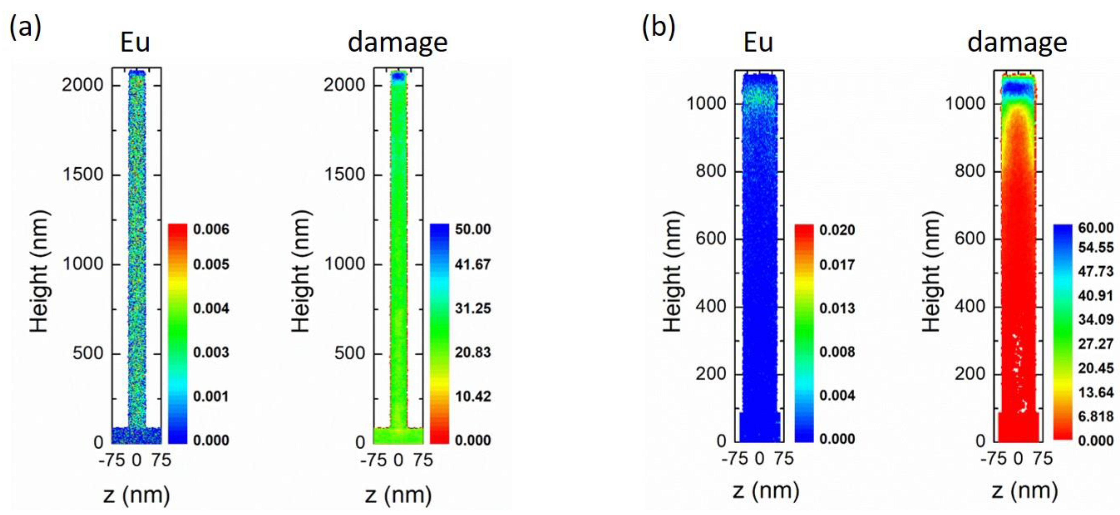
The distribution of Eu ions and implantation defects in NWs is more complex than in thin films. The results of Monte Carlo simulations, showing the Eu and defect distributions after implantation of 3 × 10¹⁵ at/cm2, are presented in Figure 4 for two different types of NWs: (a) 50 nm diameter and an areal density of 2 × 109 cm−2, and (b) 100 nm diameter and an areal density of 7 × 109 cm−2. It is clear that the final distributions depend critically on the density of the NWs and their diameter. In particular, the side facets are shadowed by surrounding NWs and the distribution of ions and defects with respect to the NW axis depends on the NW diameter. For the same implantation parameters, the first case of thinner and less dense NWs (Figure 4a) leads to homogeneous doping and defect formation in the entire NW. In contrast, for the second case of thicker and denser NWs, Eu and damage distributions are less homogeneous. In the latter case, Eu ions are confined to the top ~500 nm. A high Eu concentration is found in the top 100 nm of the NW due to ions entering through the top surface. A similar doping depth is expected for the simultaneously implanted GaN thin films. The ion range measured from the lateral surface of Eu entering through the side facets is smaller than the radius of the NWs leading to low Eu and defect concentration near the NW core and higher concentrations close to the rim.
RBS/C is not suitable for extracting implantation defect profiles in NWs. With a beam diameter of ~1 mm, the spectrum would average over a large number of NWs and due to the small tilts between individual NWs, the ion channelling is affected [59]. To study the effect of implantation on structural properties, XRD was employed. XRD allows for measuring the lattice parameters of crystals with very high resolution and is thus the technique of choice to assess strain induced by implantation defects. It is now commonly accepted that strain is one of the main driving forces for defect transformation from point defects to extended defects and eventually to amorphization [38,60,61]. Indeed, the results, presented in Section 3.1, showed that these defect transformations take place even at 15 K, suggesting that thermal effects are negligible, which agrees with the almost identical damage build-up curves at 15 K and room temperature [35].
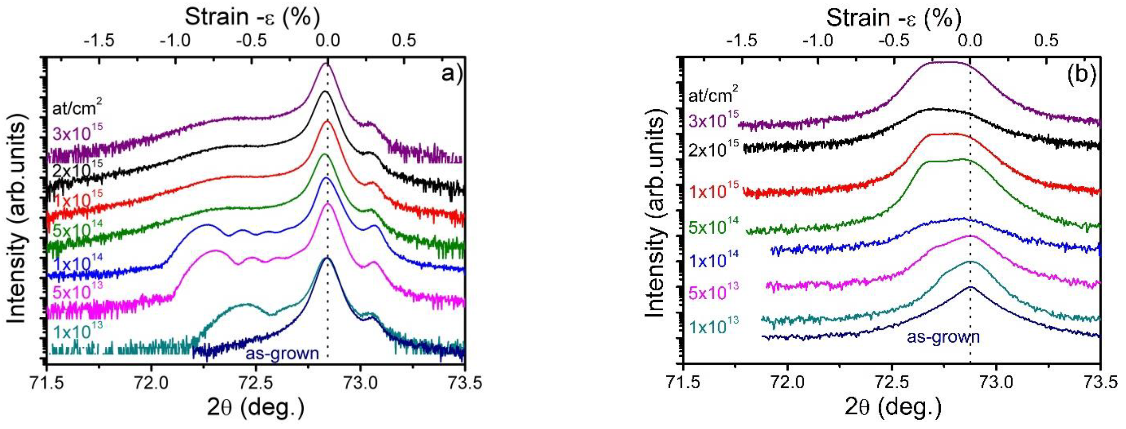
XRD 2θ−θ scans of the 0004 reflection (with θ being the Bragg angle, i.e., the angle between the incoming beam and the diffracting crystal plane) for GaN thin films and NW samples implanted using different Eu fluences are presented in Figure 5a,b, respectively [45]. The position of the main Bragg peak, corresponding to the c-lattice parameter of the as-grown material, is marked by a dotted line. It is also seen in all implanted samples arising from the unimplanted deeper layers of the crystals. For the thin films, ion implantation leads to the formation of a satellite peak at a smaller 2θ angle than the main Bragg peak. This satellite peak reveals an expansion of the c-lattice parameter of the wurtzite structure due to strain caused by the implantation defects. With increasing ion fluence, the satellite peak shifts to lower angles/higher strain until, above a fluence of 5 × 10¹⁴ at/cm2, the XRD pattern remains unchanged. In this regime, the scattered intensity is very low due to the heavily damaged crystal and the XRD technique becomes insensitive to further defect formation. The maximum strain values measured in these thin films are around 1.5% (see the upper x-axis scale in Figure 5a).
For the case of the NWs (Figure 5b), a similar expansion of the implanted volume occurs, leading to a satellite peak, which strongly overlaps with the Bragg peak of unimplanted material.
Two main differences should be pointed out compared to the results in thin films. First, the intensity ratio satellite/main Bragg peak is much higher in the NW samples than in the thin film references. This is expected since, as shown in Figure 4, the damaged volume compared to the volume of unimplanted material is higher in NWs where ions can enter through the side facets. Second, and more interestingly, the maximum strain induced in NWs stays below 0.5%. This value is much lower than in thin films, even those implanted using the lowest fluence of 1 × 10¹³ at/cm2. These results suggest that strain is more effectively dissipated in 3D NWs than in bulk material.
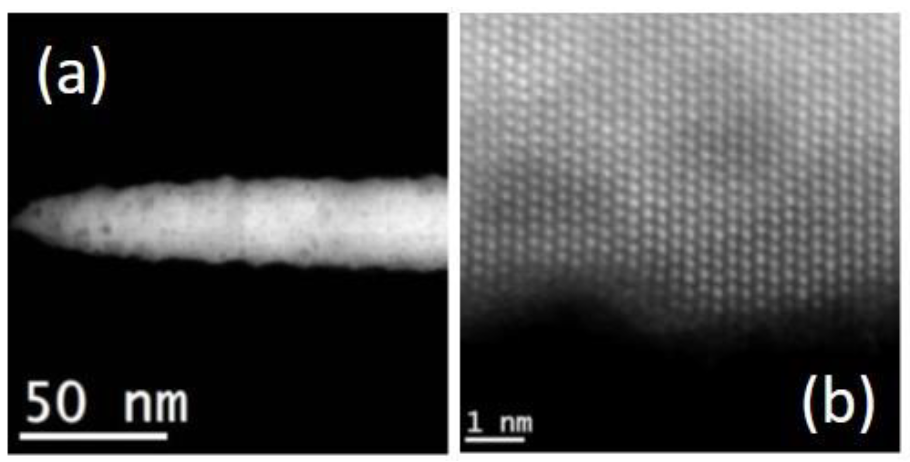
TEM high-angle annular dark-field (HAADF) images of a single NW implanted using a fluence of 1 × 10¹⁵ at/cm2 and annealed at 1000 °C are shown in Figure 6.
HAADF imaging is sensitive to the atomic number of the material (Z-contrast), thus the dark spots visible in Figure 6a are signs of thinner sample areas. Despite a high surface roughness induced by implantation/annealing, the high-resolution image in Figure 6b reveals the high crystalline quality of the NW core and the absence of the high density of extended defects typical for thin films under similar implantation and annealing conditions. In summary, one can conclude that implantation damage accumulation in NWs follows different processes than in bulk material. Strain in NWs is efficiently relaxed and one can speculate that this absence of strain inhibits the formation of the dense stacking fault network that is typical for ion implantation in GaN thin films.
3.3. Doping GaN via Ion Implantation
3.3.1. Optical Doping with Rare Earth Ions
Implanted GaN Thin Films
At LATR, Instituto Superior Técnico (Lisbon, Portugal), the most studied application of ion implantation in GaN is doping with optically active rare earth (RE) ions. Due to their partially filled 4f electron shells, which are shielded by outer filled shells, the intra-4f transitions of trivalent RE give rise to narrow and temperature-stable emission lines covering a wide range of the electromagnetic spectrum from infrared to ultraviolet [62]. In particular, by doping with different RE ions, light emission in the entire visible range can be achieved using Er or Tb for green, Eu or Pr for red and Tm for blue emissions. The work focused mostly on the red emission from Eu3+ since conventional III-nitride LEDs show very low efficiency for these long wavelengths. Recently, first successful realisation of an Eu-implanted LED structure, based on AlN nanowires with an axial p-n junction was reported, albeit still requiring relatively high voltages [63]. The first low-voltage GaN:Eu LED was reported in 2008 and was based on GaN:Eu layers doped during growth [64]. Although in situ doping avoids the drawback of implantation damage, it is prone to phase separations or clustering [65] and does not support lateral patterning.
Early work on RE implantation in GaN was reviewed in [66]. Besides the structural investigation of implantation damage, the main fields of interest were the lattice site location of RE ions in GaN, as well as their optical activation via thermal annealing. Concerning the former, one could establish that Eu is preferentially incorporated into the substitutional Ga-site or slightly displaced from it [67,68]. However, almost complete substitution is only achieved for low implantation fluences since they avoid high damage levels [45].
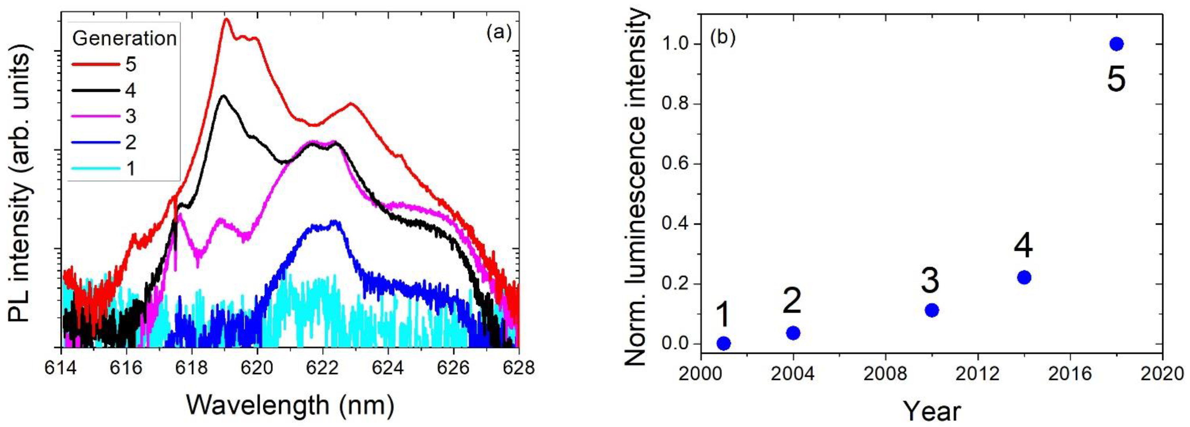
Concerning thermal annealing, it soon became clear that high annealing temperatures are the key to efficient optical activation of Eu3+. However, without appropriate protection of the surface, nitrogen starts to out-diffuse at temperatures above 800 °C, leading to the dissociation of GaN [69]. Indeed, using simple protection by applying a proximity cap (i.e., placing another GaN sample face to face with the implanted sample) and low-pressure N2 annealing atmospheres, the maximum achievable temperature was ~1000 °C [70,71]. Further research on different annealing conditions and surface protection led to several new “generations” of GaN:Eu samples with an intensity increase of the Eu3+ emission of three orders of magnitude. Figure 7 gives an overview of the photoluminescence spectra and emission intensity of these various sample generations. Generation 1 corresponds to Eu-implanted GaN annealed in N2 at ambient or low pressure. In these conditions, both furnace annealing and rapid thermal annealing can be performed up to a maximum temperature of about 1000 °C [71].
In generation 2, samples are protected using a ~10 nm thick, epitaxially grown AlN cap, allowing for annealing up to 1300 °C, above which, cracks form in the AlN cap, leading to the dissociation of the underlying GaN [72,73]. Generation 3 employs ultra-high nitrogen pressures (in the GPa range), allowing for high-temperature high pressure (HTHP) annealing up to 1400 °C [74,75]. It is interesting to note that the Eu profile is remarkably stable after annealing in these extreme conditions. However, for very high fluences, a redistribution of implanted RE is often observed [76]. For the case of Eu-implanted GaN, RBS/C results suggest that the change in the Eu profile is due to the high defect level, in particular, the dissociation of the heavily damaged surface layer [71], but reaching the solubility limits may play a role at very high annealing temperatures.
Generation 4 allows for doubling the room temperature Eu emission intensity once more using the same 1400 °C HTHP annealing but implanting into p-type Mg-doped GaN. This increase is attributed to the formation of a new optically active centre composed of an Eu–Mg cluster with a high excitation cross-section at room temperature for excitation above the GaN bandgap [77]. Finally, in generation 5, an improved furnace set-up allows for HTHP annealing at temperatures as high as 1600 °C [78].
Implanted GaN Nanowires
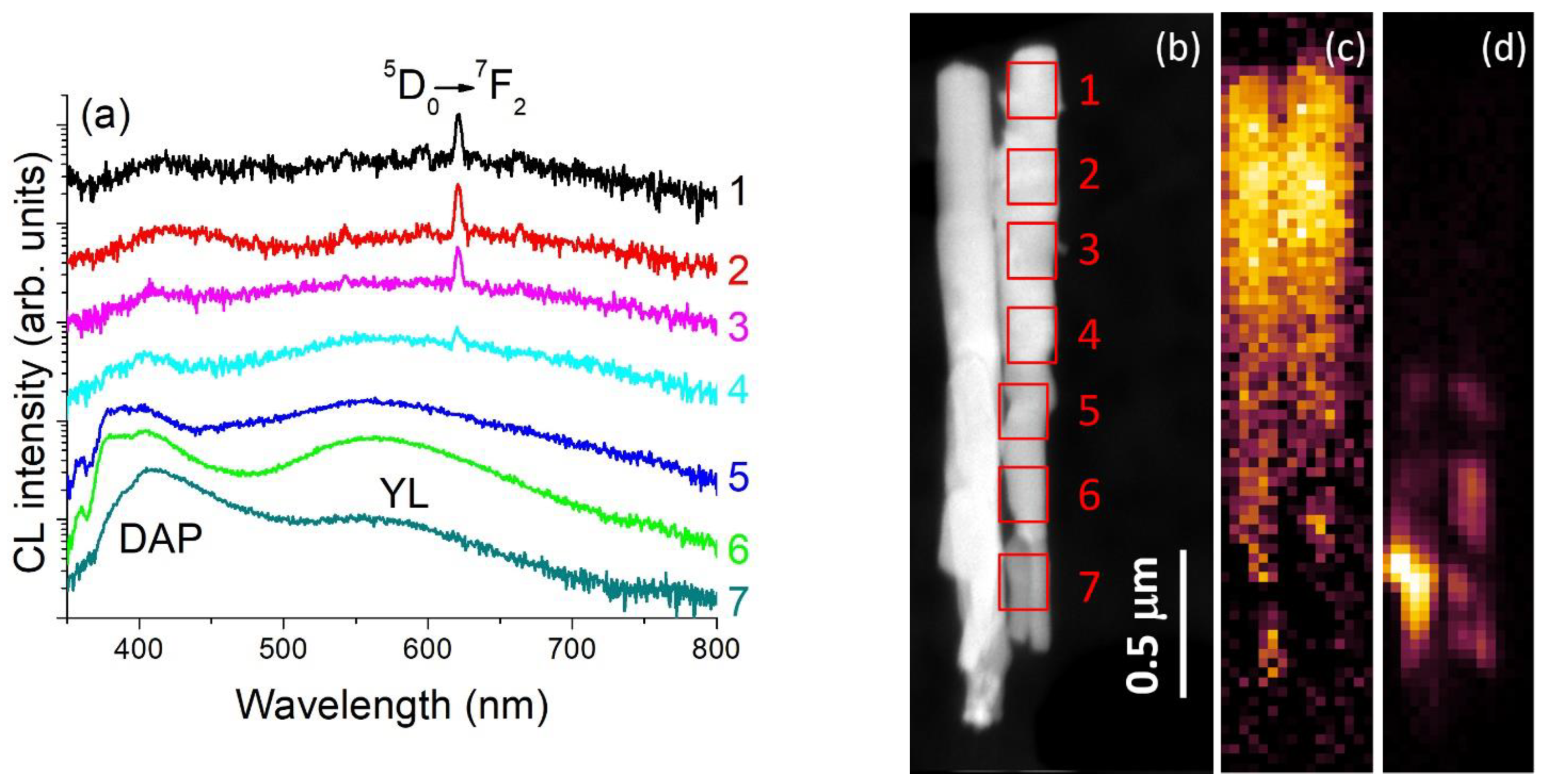
In the GaN NWs, discussed in Section 3.2, implanted Eu could be optically activated using 1000 °C rapid thermal annealing [45]. Higher annealing temperatures or longer annealing times are difficult to achieve without damaging the NWs due to their high surface-to-volume ratio, which facilitates the out-diffusion of nitrogen. Figure 8 shows nano-cathodoluminescence (CL) measurements on a single implanted NW performed in a transmission electron microscope [45]. The CL spectra in Figure 8a, taken at different spots along the NW length, show the typical Eu3+ red emission at ~620 nm from the tips of the NWs, while the base shows broad band yellow luminescence (YL) and near-band-edge emission due to donor–acceptor pairs (DAP). The mapping of the Eu-related luminescence (Figure 8c) agrees well with the MC simulations shown in Figure 4, with the most intense emission arising from the top 500 nm of the NWs where most of the Eu ions are coming to rest.
Interestingly, the luminescence intensity is higher in these NW samples than in thin-film samples implanted and annealed simultaneously. Furthermore, in thin films, a strong luminescence quenching is observed with increasing implantation fluence due to the high density of defects. In NW samples, the luminescence intensity increases monotonically with the implantation fluence, however, not at the pace expected from the increase in Eu-concentration [45]. Indeed, the measurement of the lattice site location of Eu in GaN films and nanowires using the extended X-ray absorption fine structure (EXAFS) technique revealed that Eu is predominantly incorporated on undisturbed substitutional sites only for low fluences (~1 × 10¹⁴ at/cm2). For higher fluences, an increasing number of Eu ions is found in a highly disturbed EuN-like environment where Eu is surrounded by six nitrogen atoms (instead of four, as expected for a substitutional Ga-site in GaN) [45].
3.3.2. Electrical Doping
The main electrical dopants in GaN are Si and Mg for n- and p-type doping, respectively. Si is a shallow donor, and activation percentages of ion-implanted silicon above 90% were reported quite early, typically employing a proximity cap or oxide or nitride capping layers to allow for annealing above 1000 °C [79,80]. In contrast to Si, Mg is a relatively deep dopant (with an acceptor level of 0.160 eV above the valence band), which theoretically limits the ionisation at room temperature to values smaller than 10%. Only recently, the activation of ion-implanted Mg close to this theoretical limit was reported [81,82]. Emission channelling experiments showed that implanted Mg preferentially occupies substitutional Ga sites, suggesting that low activation fractions are due to compensation by defects rather than due to interstitial incorporation [83]. Therefore, like for the optical activation of Eu, discussed in Section 3.3.1, the way to success passes through an optimisation of the annealing conditions where temperatures well above 1000 °C are required. Anderson et al. [81] used an AlN cap combined with multi-cycle annealing with a peak temperature around 1350 °C to achieve activation close to the theoretical limit. Similar multi-cycling annealing was used by Meyers et al. who furthermore showed that Mg/N co-implantation yields improved p-type conductivity, presumably due to the suppression of nitrogen vacancy formation [84]. The conversion of a low-dislocation density n-type GaN layer to p-type using Mg-implantation and the formation of a p-n junction was achieved after annealing at 1230 °C using a SiN cap [85]. Interestingly, activation of implanted Mg in nitrogen polar GaN was achieved without the need for protective capping or ultra-high pressures and allowed the fabrication of p-n junction diodes [15]. This was attributed to the increased thermal stability of this surface termination, where every N-atom at the surface is bonded to three Ga-atoms.
Similar to the Eu-activation discussed in the previous section, the best results of Mg activation were achieved by HTHP annealing at temperatures as high as 1480 °C. Acceptor activation and mobilities were shown to be close to those of epitaxial films and the surface quality was improved in comparison to AlN-capped samples [82]. In contrast to what might be expected, the high activation fraction does not necessarily imply defect-free material. Indeed, HTHP annealing at 1300 °C and 1480 °C led to the formation of extended defects after annealing. For the lower temperature, the dominant extended defect types are interstitial-type stacking faults and polarity inversion domains with Mg segregation at their boundaries. For the higher temperature, vacancy-type extended defects were observed instead [86]. The improved p-type conductivity for the higher temperature was then explained by a lower density of vacancies and their complexes which would compensate Mg acceptors, as well as reduced Mg segregation.
Eu profiles, described in Section 3.3.1, remained stable during HTHP annealing up to ~1450 °C within the uncertainties of the RBS technique. In contrast, acceptor dopants, such as Mg and Be, were shown to diffuse at these temperatures [87]. Narita et al. [88] suggested that hydrogen plays an important role in the Mg diffusion process. They determined a relatively low diffusion constant of DMg–H = 7 × 10⁻¹⁴ cm2s−1 for HPHT annealing at 1200 °C by studying diffusion from an in situ doped GaN:Mg layer into homoepitaxial GaN with a low dislocation density. For heteroepitaxial samples with higher threading dislocation density, the diffusion of implanted Mg during annealing at 1100 °C using an AlN/SiN cap is strongly dependent on the dopant concentration, with it being faster for concentrations above 1 × 10¹⁹ at/cm3. Moreover, for these high concentrations, annealing led to the formation of Mg-rich clusters [89]. Under similar annealing conditions (less than 60 min at 1100 °C using AlN-capped heteroepitaxial GaN), no diffusion of implanted Si was observed [90]. However, diffusion coefficients for silicon reported in the literature vary by several orders of magnitude and depend on the capping layer, annealing conditions and sample quality; furthermore, several distinct diffusion mechanisms can take place simultaneously [90,91,92]. Nevertheless, active dopant distributions were shown to be in good agreement with the total Si depth profiles [93].
Understanding and quantifying the diffusion of electrical dopants in GaN during post-implant annealing will be an important prerequisite for the use of ion implantation in device processing at an industrial scale. It would be interesting to study annealing techniques out of thermodynamic equilibrium, such as flash-annealing or laser-annealing in order to suppress the diffusion of dopants. Nevertheless, the recent progress in the activation of p- and n-type dopants after implantation is encouraging for the development of new device designs based on ion implantation.
4. Conclusions
In general, GaN is considered a very radiation-resistant semiconductor. This is confirmed by the strong dynamic annealing and high amorphisation thresholds revealed in the work described above and in numerous publications. However, defect dynamics upon ion implantation are very complex, leading to a mixture of different defect types, including point defects and their clusters (ranging from very small, e.g., VGaVN di- and tri-vacancies, to large clusters), as well as stacking faults and dislocation loops. This review highlights some examples of how the sample structure itself can influence the damage accumulation processes upon ion implantation. In particular, it was shown that the surface orientation of GaN layers influences the nature of extended defects created for high-fluence implantation. Basal stacking faults in the c-plane are dominant in c-plane GaN, while dislocation loops with a [110] character predominate in a-plane material. The latter also shows lower levels of randomly displaced atoms, suggesting more efficient dynamic annealing. Interestingly, extended defect formation upon ion implantation is suppressed in GaN NWs, which also shows lower defect-induced strain levels. Further defect transformation and dopant diffusion can occur during annealing, in particular, at the high temperatures needed for dopant activation in GaN. The effect of all these defect types on optical and electrical properties needs to be thoroughly understood in order to clear the way for the use of ion implantation as a routine processing technique for III-nitride devices. In this process, it should be kept in mind that there are “good” and “bad” defects. For doping, typically, the objective will be complete annealing of implantation defects or their transformation into electrically inactive defects. For implant isolation, on the other hand, the formation of thermally stable defects is a prerequisite to ensure stable properties, even after further device processing steps at high temperatures.
Funding
This research was funded by FCT Portugal, grant numbers PTDC/CTM-NAN/2156/2012, PTDC/CTM-CTM/28011/2017 and PTDC/CTM-CTM/3553/2020; Investigador FCT; and by the EU H2020 Project No. 824096 “RADIATE”.
Data Availability Statement
The data presented in this study are available on request from the corresponding author.
Acknowledgments
The above-described research would not have been possible without a huge network of dedicated and enthusiastic collaborators. I thank all my colleagues from IST who contributed to this research line with experiments, simulations, data analysis, scientific discussions and technical support: E. Alves, N. P. Barradas, F. Batista, N. Catarino, J. G. Correia, C. Cruz, D. Nd. Faye, N. Franco, M. Felizardo, M. Fialho, P. Jozwik, S. Magalhães, J. G. Marques, M. Peres, A. Redondo-Cubero, J. Rocha, M. C. Sequeira and R. C. Silva. A special thank you goes to the optical spectroscopy group of Aveiro University for 20 years of fruitful collaboration, in particular M. R. Correia, T. Monteiro, J. Rodrigues and N. Ben Sedrine. Numerous international collaborations provided access to samples and techniques otherwise not available: E. Wendler (U. Jena, in situ RBS/C); S. Schwaiger and F. Scholz (U. Ulm, nonpolar GaN growth); T. Auzelle, X. Biquard and B. Daudin (CEA Grenoble, NW growth and EXAFS analysis); M. Kociak and L. H. G. Tizei (U. Paris, nano-CL, TEM); M.-P. Chauvat, F. Gloux and P. Ruterana (U. Caen, TEM); B. Méndez and E. Nogales (Complutense University Madrid, CL); W. Möller (HZDR, 3D MC simulations in NW); M. Boćkowski (UNIPRESS, HTHP annealing); and S. Dalmasso, P. R. Edwards, R. W. Martin, K. P. O’Donnell and I. S. Roqan (U. Strathclyde, PL, CL). A special thanks to K. P. O’Donnell for the PL survey of several sample generations measured in the same conditions and shown in Figure 7.
Conflicts of Interest
The author declares no conflict of interest.
References
- The Nobel Prize in Physics 2014. NobelPrize.org. Nobel Prize Outreach AB 2021. Available online: https://www.nobelprize.org/prizes/physics/2014/summary/ (accessed on 4 October 2021).
- Taki, T.; Strassburg, M. Review—Visible LEDs: More than efficient light. ECS J. Solid State Sci. Technol. 2019, 9, 15017. [Google Scholar] [CrossRef]
- Masui, H.; Nakamura, S.; Denbaars, S.; Mishra, U.K. Nonpolar and semipolar III-nitride light-emitting diodes: Achievements and challenges. IEEE Trans. Electron Devices 2010, 57, 88–100. [Google Scholar] [CrossRef]
- Monavarian, M.; Rashidi, A.; Feezell, D. A Decade of Nonpolar and Semipolar III-Nitrides: A Review of Successes and Challenges. Phys. Status Solidi 2018, 216, 1800628. [Google Scholar] [CrossRef] [Green Version]
- Khan, A.; Balakrishnan, K.; Katona, T. Ultraviolet light-emitting diodes based on group three nitrides. Nat. Photonics 2008, 2, 77–84. [Google Scholar] [CrossRef]
- O’Donnell, K.P.; Auf der Maur, M.A.; Di Carlo, A.; Lorenz, K. It’s not easy being green: Strategies for all-nitrides, all-colour solid state lighting. Phys. Status Solidi (RRL)—Rapid Res. Lett. 2012, 6, 49–52. [Google Scholar] [CrossRef]
- Consonni, V. Self-induced growth of GaN nanowires by molecular beam epitaxy: A critical review of the formation mechanisms. Phys. Status Solidi (RRL)—Rapid Res. Lett. 2013, 7, 699–712. [Google Scholar] [CrossRef]
- Roccaforte, F.; Fiorenza, P.; Lo Nigro, R.; Giannazzo, F.; Greco, G. Physics and technology of gallium nitride materials for power electronics. Nuovo Cim. 2018, 41, 625–681. [Google Scholar] [CrossRef]
- Yu, H.; McCarthy, L.; Rajan, S.; Keller, S.; Denbaars, S.; Speck, J.; Mishra, U. Ion implanted AlGaN-GaN HEMTs with nonalloyed Ohmic contacts. IEEE Electron Device Lett. 2005, 26, 283–285. [Google Scholar] [CrossRef]
- Umeda, H.; Takizawa, T.; Anda, Y.; Ueda, T.; Tanaka, T. High-voltage isolation technique using Fe ion implantation for monolithic integration of AlGaN/GaN transistors. IEEE Trans. Electron Devices 2012, 60, 771–775. [Google Scholar] [CrossRef]
- Nanjo, T.; Takeuchi, M.; Suita, M.; Oishi, T.; Abe, Y.; Tokuda, Y.; Aoyagi, Y. Remarkable breakdown voltage enhancement in AlGaN channel high electron mobility transistors. Appl. Phys. Lett. 2008, 92, 263502. [Google Scholar] [CrossRef]
- Leonard, J.T.; Cohen, D.A.; Yonkee, B.P.; Farrell, R.M.; Margalith, T.; Lee, S.G.; DenBaars, S.P.; Speck, J.S.; Nakamura, S. Nonpolar III-nitride vertical-cavity surface-emitting lasers incorporating an ion implanted aperture. Appl. Phys. Lett. 2015, 107, 11102. [Google Scholar] [CrossRef]
- Rajabi, S.; Mandal, S.; Ercan, B.; Li, H.; Laurent, M.A.; Keller, S.; Chowdhury, S. A Demonstration of nitrogen polar gallium nitride current aperture vertical electron transistor. IEEE Electron Device Lett. 2019, 40, 885–888. [Google Scholar] [CrossRef]
- Pągowska, K.; Kozubal, M.; Taube, A.; Kruszka, R.; Kamiński, M.; Kwietniewski, N.; Juchniewicz, M.; Szerling, A. The interplay between damage- and chemical-induced isolation mechanism in Fe+-implanted AlGaN/GaN HEMT structures. Mater. Sci. Semicond. Process. 2021, 127, 105694. [Google Scholar] [CrossRef]
- Narita, T.; Kachi, T.; Kataoka, K.; Uesugi, T. P-type doping of GaN (000) by magnesium ion implantation. Appl. Phys. Express 2016, 10, 16501. [Google Scholar] [CrossRef]
- Chichibu, S.F.; Shima, K.; Kojima, K.; Takashima, S.-Y.; Ueno, K.; Edo, M.; Iguchi, H.; Narita, T.; Kataoka, K.; Ishibashi, S.; et al. Room temperature photoluminescence lifetime for the near-band-edge emission of epitaxial and ion-implanted GaN on GaN structures. Jpn. J. Appl. Phys. 2019, 58, SC0802. [Google Scholar] [CrossRef]
- Tanaka, R.; Takashima, S.; Ueno, K.; Matsuyama, H.; Edo, M.; Nakagawa, K. Mg implantation dose dependence of MOS channel characteristics in GaN double-implanted MOSFETs. Appl. Phys. Express 2019, 12, 54001. [Google Scholar] [CrossRef]
- Nomoto, K.; Tajima, T.; Mishima, T.; Satoh, M.; Nakamura, T. Remarkable reduction of on-resistance by ion implantation in GaN/AlGaN/GaN HEMTs with low gate leakage current. IEEE Electron Device Lett. 2007, 28, 939–941. [Google Scholar] [CrossRef]
- Nanjo, T.; Takeuchi, M.; Suita, M.; Abe, Y.; Oishi, T.; Tokuda, Y.; Aoyagi, Y. First operation of AlGaN channel high electron mobility transistors. Appl. Phys. Express 2008, 1, 11101. [Google Scholar] [CrossRef]
- Mandal, S.; Agarwal, A.; Ahmadi, E.; Bhat, K.M.; Ji, D.; Laurent, M.A.; Keller, S.; Chowdhury, S. Dispersion free 450-V p GaN-gated CAVETs with Mg-ion implanted blocking layer. IEEE Electron. Device Lett. 2017, 38, 933–936. [Google Scholar] [CrossRef]
- Ji, D.; Agarwal, A.; Li, W.; Keller, S.; Chowdhury, S. Demonstration of GaN current aperture vertical electron transistors with aperture region formed by ion implantation. IEEE Trans. Electron Devices 2018, 65, 483–487. [Google Scholar] [CrossRef]
- Ji, D.; Li, S.; Ercan, B.; Ren, C.; Chowdhury, S. Design and fabrication of ion-implanted moat etch termination resulting in 0.7 mΩ⋅cm2/1500 V GaN Diodes. IEEE Electron Device Lett. 2020, 41, 264–267. [Google Scholar] [CrossRef]
- Tanaka, R.; Takashima, S.; Ueno, K.; Matsuyama, H.; Edo, M. Demonstration of 1200 V/1.4 mΩcm2 vertical GaN planar MOSFET fabricated by an all ion implantation process. Jpn. J. Appl. Phys. 2020, 59, SGGD02. [Google Scholar] [CrossRef]
- Yoshino, M.; Ando, Y.; Deki, M.; Toyabe, T.; Kuriyama, K.; Honda, Y.; Nishimura, T.; Amano, H.; Kachi, T.; Nakamura, T. Fully ion implanted normally-Off GaN DMOSFETs with ALD-Al2O3 gate dielectrics. Materials 2019, 12, 689. [Google Scholar] [CrossRef] [PubMed] [Green Version]
- Ozbek, A.M.; Baliga, B.J. Planar nearly ideal edge-termination technique for GaN devices. IEEE Electron Device Lett. 2011, 32, 300–302. [Google Scholar] [CrossRef]
- Zhang, Y.; Sun, M.; Wong, H.-Y.; Lin, Y.; Srivastava, P.; Hatem, C.; Azize, M.; Piedra, D.; Yu, L.; Sumitomo, T.; et al. Origin and control of OFF-state leakage current in GaN-on-Si vertical diodes. IEEE Trans. Electron Devices 2015, 62, 2155–2161. [Google Scholar] [CrossRef] [Green Version]
- Taube, A.; Kamińska, E.; Kozubal, M.; Kaczmarski, J.; Wojtasiak, W.; Jasiński, J.; Borysiewicz, M.A.; Ekielski, M.; Juchniewicz, M.; Grochowski, J.; et al. Ion implantation for isolation of AlGaN/GaN HEMTs using C or Al. Phys. Status Solidi 2015, 212, 1162–1169. [Google Scholar] [CrossRef]
- Sun, S.; Fu, K.; Yu, G.; Zhang, Z.; Song, L.; Deng, X.; Qi, Z.; Li, S.; Su, Q.; Cai, Y.; et al. AlGaN/GaN metal-insulator-semiconductor high electron mobility transistors with reduced leakage current and enhanced breakdown voltage using aluminum ion implantation. Appl. Phys. Lett. 2016, 108, 13507. [Google Scholar] [CrossRef]
- Iucolano, F.; Giannazzo, F.; Roccaforte, F.; Romano, L.; Grimaldi, M.; Raineri, V. Quantitative determination of depth carrier profiles in ion-implanted Gallium Nitride. Nucl. Instrum. Methods Phys. Res. Sect. B Beam Interact. Mater. Atoms 2007, 257, 336–339. [Google Scholar] [CrossRef]
- Pankove, J.I.; Hutchby, J.A. Photoluminescence of ion-implanted GaN. J. Appl. Phys. 1976, 47, 5387–5390. [Google Scholar] [CrossRef]
- Ronning, C. Ion implantation into gallium nitride. Phys. Rep. 2001, 351, 349–385. [Google Scholar] [CrossRef]
- Kucheyev, S.; Williams, J.; Pearton, S. Ion implantation into GaN. Mater. Sci. Eng. R Rep. 2001, 33, 51–108. [Google Scholar] [CrossRef]
- Lorenz, K.; Wendler, E. Implantation damage formation in GaN and ZnO. In Ion Implantation; Goorsky, M.S., Ed.; InTech: London, UK, 2012; pp. 237–264. Available online: http://www.issp.ac.ru/ebooks/books/open/Ion_Implantation.pdf (accessed on 20 April 2022).
- Turos, A. On the mechanism of damage buildup in gallium nitride. Radiat. Eff. Defects Solids 2013, 168, 431–441. [Google Scholar] [CrossRef]
- Wendler, E.; Wesch, W.; Azarov, A.; Catarino, N.; Redondo-Cubero, A.; Alves, E.; Lorenz, K. Comparison of low- and room-temperature damage formation in Ar ion implanted GaN and ZnO. Nucl. Instrum. Methods Phys. Res. Sect. B Beam Interact. Mater. Atoms 2013, 307, 394–398. [Google Scholar] [CrossRef]
- Titov, A.I.; Karabeshkin, K.V.; Struchkov, A.I.; Karaseov, P.A.; Azarov, A. Radiation tolerance of GaN: The balance between radiation-stimulated defect annealing and defect stabilization by implanted atoms. J. Phys. D Appl. Phys. 2022, 55, 175103. [Google Scholar] [CrossRef]
- Lorenz, K.; Peres, M.; Franco, N.; Marques, J.G.; Miranda, S.M.C.; Magalhães, S.; Monteiro, T.; Wesch, W.; Alves, E.; Wendler, E. Radiation damage formation and annealing in GaN and ZnO. In Proceedings of the SPIE OPTO 2011, San Francisco, CA, USA, 22–27 January 2011; Volume 7940, p. 79400O. [Google Scholar] [CrossRef]
- Pągowska, K.; Ratajczak, R.; Stonert, A.; Turos, A.; Nowicki, L.; Sathish, N.; Jóźwik, P.; Muecklich, A. RBS/Channeling and TEM study of damage buildup in ion bombarded GaN. Acta Phys. Pol. A 2011, 120, 153–155. [Google Scholar] [CrossRef]
- Ruterana, P.; Lacroix, B.; Lorenz, K. A mechanism for damage formation in GaN during rare earth ion implantation at medium range energy and room temperature. J. Appl. Phys. 2011, 109, 13506. [Google Scholar] [CrossRef] [Green Version]
- Kucheyev, S.O.; Williams, J.S.; Zou, J.; Jagadish, C. Dynamic annealing in III-nitrides under ion bombardment. J. Appl. Phys. 2004, 95, 3048–3054. [Google Scholar] [CrossRef] [Green Version]
- Leclerc, S.; Lacroix, B.; Declémy, A.; Lorenz, K.; Ruterana, P. Mechanisms of damage formation in Eu-implanted AlN. J. Appl. Phys. 2012, 112, 73525. [Google Scholar] [CrossRef] [Green Version]
- Li, B.; Liu, H.; Lu, X.; Kang, L.; Sheng, Y.; Xiong, A. Atomic configurations of basal stacking faults and dislocation loops in GaN irradiated with Xe20+ ions at room temperature. Appl. Surf. Sci. 2019, 486, 15–21. [Google Scholar] [CrossRef]
- Alves, E.; Lorenz, K.; Catarino, N.; Peres, M.; Dias, M.; Mateus, R.; Alves, L.C.; Corregidor, V.; Barradas, N.P.; Fonseca, M.; et al. An insider view of the Portuguese Ion Beam Laboratory. Eur. Phys. J. Plus 2021, 136, 684. [Google Scholar] [CrossRef]
- Lorenz, K.; Wendler, E.; Redondo-Cubero, A.; Catarino, N.; Chauvat, M.-P.; Schwaiger, S.; Scholz, F.; Alves, E.; Ruterana, P. Implantation damage formation in a-, c- and m-plane GaN. Acta Mater. 2017, 123, 177–187. [Google Scholar] [CrossRef]
- Faye, D.N.; Biquard, X.; Nogales, E.; Felizardo, M.; Peres, M.; Redondo-Cubero, A.; Auzelle, T.; Daudin, B.; Tizei, L.H.; Kociak, M.; et al. Incorporation of europium into GaN nanowires by ion implantation. J. Phys. Chem. C 2019, 123, 11874–11887. [Google Scholar] [CrossRef]
- Auzelle, T.; Haas, B.; Minj, A.; Bougerol, C.; Rouvière, J.-L.; Cros, A.; Colchero, J.; Daudin, B. The influence of AlN buffer over the polarity and the nucleation of self-organized GaN nanowires. J. Appl. Phys. 2015, 117, 245303. [Google Scholar] [CrossRef]
- Jozwik, P.; Nowicki, L.; Ratajczak, R.; Stonert, A.; Mieszczynski, C.; Turos, A.; Morawiec, K.; Lorenz, K.; Alves, E. Monte Carlo simulations of ion channeling in crystals containing dislocations and randomly displaced atoms. J. Appl. Phys. 2019, 126, 195107. [Google Scholar] [CrossRef]
- Lorenz, K.; Barradas, N.P.; Alves, E.; Roqan, I.S.; Nogales, E.; Martin, R.W.; O’Donnell, K.P.; Gloux, F.; Ruterana, P. Structural and optical characterization of Eu-implanted GaN. J. Phys. D: Appl. Phys. 2009, 42, 165103. [Google Scholar] [CrossRef]
- Hecking, N.; Heidemann, K.; Kaat, E.T. Model of temperature dependent defect interaction and amorphization in crystalline silicon during ion irradiation. Nucl. Instrum. Methods Phys. Res. Sect. B Beam Interact. Mater. Atoms 1986, 15, 760–764. [Google Scholar] [CrossRef]
- Wendler, E.; Kamarou, A.; Alves, E.; Gärtner, K.; Wesch, W. Three-step amorphisation process in ion-implanted GaN at 15 K. Nucl. Instrum. Methods Phys. Res. Sect. B Beam Interact. Mater. Atoms 2003, 206, 1028–1032. [Google Scholar] [CrossRef]
- Faye, D.N.; Wendler, E.; Felizardo, M.; Magalhaes, S.; Alves, E.; Brunner, F.; Weyers, M.; Lorenz, K. Mechanisms of implantation damage formation in AlxGa1–xN compounds. J. Phys. Chem. C 2016, 120, 7277–7283. [Google Scholar] [CrossRef]
- Kucheyev, S.O.; Azarov, A.Y.; Titov, A.I.; Karaseov, P.A.; Kuchumova, T.M. Energy spike effects in ion-bombarded GaN. J. Phys. D Appl. Phys. 2009, 42, 85309. [Google Scholar] [CrossRef]
- Kucheyev, S.O.; Williams, J.S.; Jagadish, C.; Zou, J.; Li, G.; Titov, A.I. Effect of ion species on the accumulation of ion-beam damage in GaN. Phys. Rev. B 2001, 64, 35202. [Google Scholar] [CrossRef] [Green Version]
- Biersack, J.P.; Ziegler, J.F. The stopping and range of ions in solids. In Ion Implantation Techniques; Ryssel, H., Glawischnig, H., Eds.; Springer: Berlin/Heidelberg, Germany, 1982; pp. 122–156. [Google Scholar] [CrossRef]
- Macková, A.; Malinský, P.; Jagerová, A.; Mikšová, R.; Sofer, Z.; Klímová, K.; Mikulics, M.; Böttger, R.; Akhmadaliev, S.; Oswald, J. Damage accumulation and implanted Gd and Au position in a- and c-plane GaN. Thin Solid Film. 2019, 680, 102–113. [Google Scholar] [CrossRef]
- Catarino, N.; Nogales, E.; Franco, N.; Darakchieva, V.; Miranda, S.M.C.; Méndez, B.; Alves, E.; Marques, J.G.; Lorenz, K. Enhanced dynamic annealing and optical activation of Eu implanted a-plane GaN. Europhys. Lett. 2012, 97, 68004. [Google Scholar] [CrossRef]
- Turos, A.; Jóźwik, P.; Wójcik, M.; Gaca, J.; Ratajczak, R.; Stonert, A. Mechanism of damage buildup in ion bombarded ZnO. Acta Mater. 2017, 134, 249–256. [Google Scholar] [CrossRef]
- Lacroix, B.; Leclerc, S.; Declemy, A.; Lorenz, K.; Alves, E.; Ruterana, P. Mechanisms of damage formation in Eu-implanted GaN probed by X-ray diffraction. Europhys. Lett. 2011, 96, 46002. [Google Scholar] [CrossRef]
- Lorenz, K.; Nogales, E.; Miranda, S.; Franco, N.; Méndez, B.; Alves, E.; Tourbot, G.; Daudin, B. Enhanced red emission from praseodymium-doped GaN nanowires by defect engineering. Acta Mater. 2013, 61, 3278–3284. [Google Scholar] [CrossRef]
- Debelle, A.; Crocombette, J.-P.; Boulle, A.; Chartier, A.; Jourdan, T.; Pellegrino, S.; Bachiller-Perea, D.; Carpentier, D.; Channagiri, J.; Nguyen, T.-H.; et al. Lattice strain in irradiated materials unveils a prevalent defect evolution mechanism. Phys. Rev. Mater. 2018, 2, 13604. [Google Scholar] [CrossRef] [Green Version]
- Mendes, P.; Lorenz, K.; Alves, E.; Schwaiger, S.; Scholz, F.; Magalhães, S. Measuring strain caused by ion implantation in GaN. Mater. Sci. Semicond. Process. 2019, 98, 95–99. [Google Scholar] [CrossRef]
- O’Donnell, K.P.; Hourahine, B. Rare earth doped III-nitrides for optoelectronics. Eur. Phys. J. Appl. Phys. 2006, 36, 91–103. [Google Scholar] [CrossRef] [Green Version]
- Cardoso, J.P.S.; Correia, M.R.; Vermeersch, R.; Verheij, D.; Jacopin, G.; Pernot, J.; Monteiro, T.; Cardoso, S.; Lorenz, K.; Daudin, B.; et al. Europium-implanted AlN nanowires for red light-emitting diodes. ACS Appl. Nano Mater. 2022, 5, 972–984. [Google Scholar] [CrossRef]
- Nishikawa, A.; Kawasaki, T.; Furukawa, N.; Terai, Y.; Fujiwara, Y. Room-temperature red emission from a p-type/europium-doped/n-type gallium nitride light-emitting diode under current injection. Appl. Phys. Express 2009, 2, 71004. [Google Scholar] [CrossRef]
- Lorenz, K.; Alves, E.; Roqan, I.S.; O’Donnell, K.P.; Nishikawa, A.; Fujiwara, Y.; Boćkowski, M. Lattice site location of optical centers in GaN:Eu light emitting diode material grown by organometallic vapor phase epitaxy. Appl. Phys. Lett. 2010, 97, 111911. [Google Scholar] [CrossRef] [Green Version]
- Lorenz, K.; Alves, E.; Gloux, F.; Ruterana, P. RE implantation and annealing of III-nitrides. In Rare Earth Doped III-Nitrides for Optoelectronic and Spintronic Applications; O’Donnell, K., Dierolf, V., Eds.; Springer: Dordrecht, Germany, 2010; pp. 25–54. [Google Scholar] [CrossRef]
- Alves, E.; Lorenz, K.; Vianden, R.; Boemare, C.; Soares, M.J.; Monteiro, T. Optical doping of nitrides by ion implantation. Mod. Phys. Lett. B 2001, 15, 1281–1287. [Google Scholar] [CrossRef] [Green Version]
- Wahl, U.; Alves, E.; Lorenz, K.; Correia, J.; Monteiro, T.; De Vries, B.; Vantomme, A.; Vianden, R. Lattice location and optical activation of rare earth implanted GaN. Mater. Sci. Eng. B 2003, 105, 132–140. [Google Scholar] [CrossRef] [Green Version]
- Karpiński, J.; Jun, J.; Porowski, S. Equilibrium pressure of N2 over GaN and high pressure solution growth of GaN. J. Cryst. Growth 1984, 66, 1–10. [Google Scholar] [CrossRef]
- Alves, E.; Da Silva, M.; Marques, J.; Soares, J.; Freitag, K. Annealing behavior and lattice site location of Hf implanted GaN. Mater. Sci. Eng. B 1999, 59, 207–210. [Google Scholar] [CrossRef]
- Lorenz, K.; Wahl, U.; Alves, E.; Nogales, E.; Dalmasso, S.; Martin, R.; O’Donnell, K.; Wojdak, M.; Braud, A.; Monteiro, T.; et al. High temperature annealing of rare earth implanted GaN films: Structural and optical properties. Opt. Mater. 2006, 28, 750–758. [Google Scholar] [CrossRef]
- Lorenz, K.; Wahl, U.; Alves, E.; Dalmasso, S.; Martin, R.W.; O’Donnell, K.P.; Ruffenach, S.; Briot, O. High-temperature annealing and optical activation of Eu-implanted GaN. Appl. Phys. Lett. 2004, 85, 2712–2714. [Google Scholar] [CrossRef]
- Nogales, E.; Martin, R.W.; O’Donnell, K.P.; Lorenz, K.; Alves, E.; Ruffenach, S.; Briot, O. Failure mechanism of AlN nanocaps used to protect rare earth-implanted GaN during high temperature annealing. Appl. Phys. Lett. 2006, 88, 31902. [Google Scholar] [CrossRef] [Green Version]
- Lorenz, K.; Miranda, S.M.C.; Alves, E.; Roqan, I.S.; O’Donnell, K.P.; Boćkowski, M. High pressure annealing of Europium implanted GaN. In Proceedings of the SPIE OPTO 2012, San Francisco, CA, USA, 21–26 January 2012; Volume 8262, p. 82620C. [Google Scholar] [CrossRef] [Green Version]
- Roqan, I.S.; O’Donnell, K.P.; Martin, R.W.; Edwards, P.R.; Song, S.F.; Vantomme, A.; Lorenz, K.; Alves, E.; Bockowski, M. Identification of the prime optical center in GaN:Eu3+. Phys. Rev. B 2010, 81, 85209. [Google Scholar] [CrossRef]
- Mackova, A.; Malinský, P.; Sofer, Z.; Šimek, P.; Sedmidubský, D.; Mikulics, M.; Wilhelm, R. A study of the structural properties of GaN implanted by various rare earth ions. Nucl. Instrum. Methods Phys. Res. Sect. B Beam Interact. Mater. Atoms 2013, 307, 446–451. [Google Scholar] [CrossRef]
- O’Donnell, K.P.; Edwards, P.R.; Yamaga, M.; Lorenz, K.; Kappers, M.J.; Bockowski, M. Crystalfield symmetries of luminescent Eu3+ centers in GaN: The importance of the 5D0 to 7F1 transition. Appl. Phys. Lett. 2016, 108, 22102. [Google Scholar] [CrossRef] [Green Version]
- Singh, A.; O’Donnell, K.P.; Edwards, P.R.; Cameron, D.; Lorenz, K.; Kappers, M.J.; Bockowski, M.; Yamaga, M.; Prakash, R. Luminescence of Eu3+ in GaN(Mg, Eu): Transitions from the 5D1 level. Appl. Phys. Lett. 2017, 111, 241105. [Google Scholar] [CrossRef] [Green Version]
- Pearton, S.J.; Vartuli, C.B.; Zolper, J.C.; Yuan, C.; Stall, R.A. Ion implantation doping and isolation of GaN. Appl. Phys. Lett. 1995, 67, 1435–1437. [Google Scholar] [CrossRef]
- Irokawa, Y.; Fujishima, O.; Kachi, T.; Nakano, Y. Electrical activation characteristics of silicon-implanted GaN. J. Appl. Phys. 2005, 97, 83505. [Google Scholar] [CrossRef]
- Anderson, T.; Feigelson, B.; Kub, F.; Tadjer, M.; Hobart, K.; Mastro, M.; Hite, J.; Eddy, C. Activation of Mg implanted in GaN by multicycle rapid thermal annealing. Electron. Lett. 2014, 50, 197–198. [Google Scholar] [CrossRef]
- Bockowski, M.; Omori, M.; Yamada, S.; Furukawa, Y.; Suzuki, H.; Narita, T.; Kataoka, K.; Horita, M.; Suda, J.; Kachi, T. Highly effective activation of Mg-implanted p-type GaN by ultra-high-pressure annealing. Appl. Phys. Lett. 2019, 115, 142104. [Google Scholar] [CrossRef]
- Wahl, U.; Amorim, L.M.; Augustyns, V.; Costa, A.; David-Bosne, E.; Lima, T.A.L.; Lippertz, G.; Correia, J.G.; da Silva, M.R.; Kappers, M.J.; et al. Lattice location of Mg in GaN: A fresh look at doping limitations. Phys. Rev. Lett. 2017, 118, 95501. [Google Scholar] [CrossRef] [Green Version]
- Meyers, V.; Rocco, E.; Hogan, K.; McEwen, B.; Shevelev, M.; Sklyar, V.; Jones, K.; Derenge, M.; Shahedipour-Sandvik, F. P-type conductivity and suppression of green luminescence in Mg/N co-implanted GaN by gyrotron microwave annealing. J. Appl. Phys. 2021, 130, 85704. [Google Scholar] [CrossRef]
- Oikawa, T.; Saijo, Y.; Kato, S.; Mishima, T.; Nakamura, T. Formation of definite GaN p-n junction by Mg-ion implantation to n−-GaN epitaxial layers grown on a high-quality free-standing GaN substrate. Nucl. Instrum. Methods Phys. Res. Sect. B Beam Interact. Mater. Atoms 2015, 365, 168–170. [Google Scholar] [CrossRef]
- Iwata, K.; Sakurai, H.; Arai, S.; Nakashima, T.; Narita, T.; Kataoka, K.; Bockowski, M.; Nagao, M.; Suda, J.; Kachi, T.; et al. Defect evolution in Mg ions implanted GaN upon high temperature and ultrahigh N2 partial pressure annealing: Transmission electron microscopy analysis. J. Appl. Phys. 2020, 127, 105106. [Google Scholar] [CrossRef]
- Sierakowski, K.; Jakiela, R.; Lucznik, B.; Kwiatkowski, P.; Iwinska, M.; Turek, M.; Sakurai, H.; Kachi, T.; Bockowski, M. High pressure processing of ion implanted GaN. Electronics 2020, 9, 1380. [Google Scholar] [CrossRef]
- Narita, T.; Sakurai, H.; Bockowski, M.; Kataoka, K.; Suda, J.; Kachi, T. Electric-field-induced simultaneous diffusion of Mg and H in Mg-doped GaN prepared using ultra-high-pressure annealing. Appl. Phys. Express 2019, 12, 111005. [Google Scholar] [CrossRef]
- Lardeau-Falcy, A.; Amichi, L.; Coig, M.; Kanyandekwe, J.; Milesi, F.; Grenier, A.; Veillerot, M.; Eymery, J.; Mazen, F. Diffusion and aggregation of Mg implanted in GaN on Si. In Proceedings of the 2018 22nd International Conference on Ion Implantation Technology (IIT), Würzburg, Germany, 16–21 September 2018; pp. 74–77. [Google Scholar] [CrossRef]
- Jakiela, R.; Barcz, A.; Dumiszewska, E.; Jagoda, A. Si diffusion in epitaxial GaN. Phys. Status Solidi 2006, 3, 1416–1419. [Google Scholar] [CrossRef]
- Pan, C.J.; Chi, G.C.; Pong, B.J.; Sheu, J.K.; Chen, J.Y. Si diffusion in p-GaN. J. Vac. Sci. Technol. B Microelectron. Nanometer Struct. 2004, 22, 1727. [Google Scholar] [CrossRef]
- Ostermaier, C.; Ahn, S.-I.; Potzger, K.; Helm, M.; Kuzmik, J.; Pogany, D.; Strasser, G.; Lee, J.-H.; Hahm, S.-H.; Lee, J.-H. Study of Si implantation into Mg-doped GaN for MOSFETs. Phys. Status Solidi 2010, 7, 1964–1966. [Google Scholar] [CrossRef]
- Lamhamdi, M.; Cayrel, F.; Bazin, A.; Collard, E.; Alquier, D. Carrier profiling in Si-implanted gallium nitride by Scanning Capacitance Microscopy. Nucl. Instrum. Methods Phys. Res. Sect. B Beam Interact. Mater. Atoms 2011, 275, 37–40. [Google Scholar] [CrossRef]
Figure 1.
(a) Wurtzite GaN structure and major crystallographic planes. (b) Schematic sample structures with a- and c-plane GaN grown using metal-organic vapour-phase epitaxy (MOVPE) and the m-plane sample using hydride vapour-phase epitaxy (HVPE). (c) Scanning electron microscopy (SEM) image of the molecular beam epitaxy (MBE) grown nanowires (NWs).

Figure 2.
(a) Rutherford backscattering spectrometry/channelling (RBS/C) aligned spectra for a-plane GaN samples implanted using different fluences (only some of which are indicated in the legend for clarity) of 300 keV Ar at 15 K. The random spectrum for the sample implanted to the highest fluence is also shown. (b) Relative defect level as a function of the implantation fluence for a-, c- and m-plane samples. The solid lines are fits using the Hecking model. Adapted with permission from Ref. [44].

Figure 3.
Cross-sectional transmission electron microscopy (TEM) images of c-plane GaN (a) and a-plane GaN (b) implanted with 300 keV Ar using a fluence of 8 × 10¹⁵ at/cm2. The defect profiles derived using RBS/C were superimposed onto the TEM images. In (b), a large density of dislocation loops can be observed, some of which are marked by yellow arrows. Adapted with permission from Ref. [44].

Figure 4.
Monte Carlo simulations showing the Eu atomic fraction within the NW, as well as the damage distribution (in displacements per atom) in a longitudinal slice of 8 nm thickness along the NW length for the implantation of 3 × 10¹⁵ at/cm2 Eu ions at 300 keV and incidence angle of 20°. (a) For an array of 50 nm diameter NWs with an areal density of 2 × 109 cm−2; (b) for an array of 100 nm diameter and an areal density of 7 × 109 cm−2. Adapted with permission from Ref. [45].

Figure 5.
X−ray diffraction 2θ−θ scans (θ being the Bragg angle) of the 0004 reflection of c-plane GaN thin films (a) and GaN NWs (b) before and after implantation with different Eu fluences at 300 keV and 20° incident angle. The dotted line marks the main Bragg peak corresponding to the unimplanted volume of the crystal. Note that the small peak at 2θ = 73.05° is due to residual Kα2 radiation that was not completely removed by the monochromator. Reprinted with permission from Ref. [45].

Figure 6.
(a) TEM HAADF (high-angle annular dark-field) image of an NW implanted using a fluence of 1 × 10¹⁵ at/cm2 and annealed at 1000 °C. (b) High-resolution TEM HAADF images of the same NW show a high crystalline quality of the NW core. Adapted with permission from Ref. [45].
Figure 6.
(a) TEM HAADF (high-angle annular dark-field) image of an NW implanted using a fluence of 1 × 10¹⁵ at/cm2 and annealed at 1000 °C. (b) High-resolution TEM HAADF images of the same NW show a high crystalline quality of the NW core. Adapted with permission from Ref. [45].

Figure 7.
Typical RT photoluminescence (PL) spectra (a) and normalised RT luminescence intensity (b) for the five generations of Eu-implanted GaN. Generation 1: simple furnace annealing or rapid thermal annealing at ~1000 °C; generation 2: AlN capping allows annealing up to ~1300 °C; generation 3: HTHP annealing up to 1400 °C; generation 4: Mg co-doping and HTHP annealing up to 1400 °C; generation 5: Mg co-doping and HTHP annealing up to 1600 °C.

Figure 8.
(a) Nano-cathodoluminescence (CL) spectra taken at seven points from the top (1) to the bottom (7) of a single NW implanted using a fluence of 1 × 10¹⁴ at/cm2 (20° incidence angle) and annealed at 1000 °C. The regions where the spectra were taken are indicated with red rectangles in (b). ‘’DAP’’ denotes donor–acceptor pairs and ‘’YL’’ stays for yellow luminescence. (c,d) Luminescence intensity maps integrating the spectra in a wavelength region around the 622 nm Eu3+ line (c) and from 350 to 550 nm (d). Adapted with permission from Ref. [45].

Publisher’s Note: MDPI stays neutral with regard to jurisdictional claims in published maps and institutional affiliations. |
© 2022 by the author. Licensee MDPI, Basel, Switzerland. This article is an open access article distributed under the terms and conditions of the Creative Commons Attribution (CC BY) license (https://creativecommons.org/licenses/by/4.0/).
Share and Cite
MDPI and ACS Style
Lorenz, K. Ion Implantation into Nonconventional GaN Structures. Physics 2022, 4, 548-564. https://0-doi-org.brum.beds.ac.uk/10.3390/physics4020036
AMA Style
Lorenz K. Ion Implantation into Nonconventional GaN Structures. Physics. 2022; 4(2):548-564. https://0-doi-org.brum.beds.ac.uk/10.3390/physics4020036
Chicago/Turabian StyleLorenz, Katharina. 2022. "Ion Implantation into Nonconventional GaN Structures" Physics 4, no. 2: 548-564. https://0-doi-org.brum.beds.ac.uk/10.3390/physics4020036