Technology for SMD Packaging MOX Gas Sensors †
by
Nikolay Samotaev
*, 
Konstantin Oblov
,
Anastasia Ivanova
,
Boris Podlepetsky
,
Nikolay Volkov
and
Nazar Zibilyuk
National Research Nuclear University MEPhI (Moscow Engineering Physics Institute), Kashirskoe Highway 31, 115409 Moscow, Russia
*
Author to whom correspondence should be addressed.
†
Presented at the Eurosensors 2018 Conference, Graz, Austria, 9–12 September 2018.
Proceedings 2018, 2(13), 934; https://0-doi-org.brum.beds.ac.uk/10.3390/proceedings2130934
Published: 30 November 2018
(This article belongs to the Proceedings of EUROSENSORS 2018)
Abstract
:The perspective combination of laser micromilling technology and jet (aerosol) printing technologies for ceramic MEMS producing of microhotplate in the surface mounted device (SMD) package for the metal oxide (MOX) sensor is describing. There are discusses technological and economic aspects of small-scale production of gas MOX sensors. Experiments with laser micromilling of Al2O3 ceramics confirmed possibility to produce MEMS microhotplate for MOX gas sensor in SMD package with form-factor SOT-23. Developed technology process is close to 3D prototype philosophy—rapid, simple and cheap.
1. Introduction
The modern MOX sensor is a combination of several factors—a microhotplate (responsible for power consumption and temperature operation mode), MOX gas sensitive layer (responsible for sensitivity to target gases) and a package (responsible for the possible applications of MOX gas sensor) [1]. Last decades MOX gas sensors development there is a concentration of efforts, in the field of technologies allowing obtaining a cheap product for mass applications in the manner of indoor air quality monitoring. Similar solutions were found by the leading manufacturers of MOX sensors (Figaro, Sensirion, Bosch, AMS, SGX, etc.) [2,3,4,5,6]. Technological solutions that make it possible to obtain a sensor with satisfactory characteristics for such application consist in the use of a combination of silicon MEMS microhotplate [2,3,4,5,6] and plastic [2,3], metal-plastic [4] or metal-ceramic [5,6] SMD package. But what need to do scientific groups which, at the moment there is no market or market still small for the return of investment in silicon MEMS technology and the production of specialized plastic or ceramic SMD package? In that case need using technology process close to 3D-prototype philosophy—rapid, simple and cheap with ratio a single sample to total production cost.
After several experiments with wide spectres ceramics MEMS technologies and materials (ZrO2 [7], Al2O3 [8], LTCC ceramics [9]) we find more flexible technology responsible to goals of 3D prototype philosophy. As a technology for manufacturing ceramic MEMS MOX sensor and SMD package for one, we propose to use combination of laser micromilling monolithic Al2O3 commercially available ceramics and screen-print/jet (aerosol) printing technologies to form platinum metallization on MEMS and package.
2. Experiment
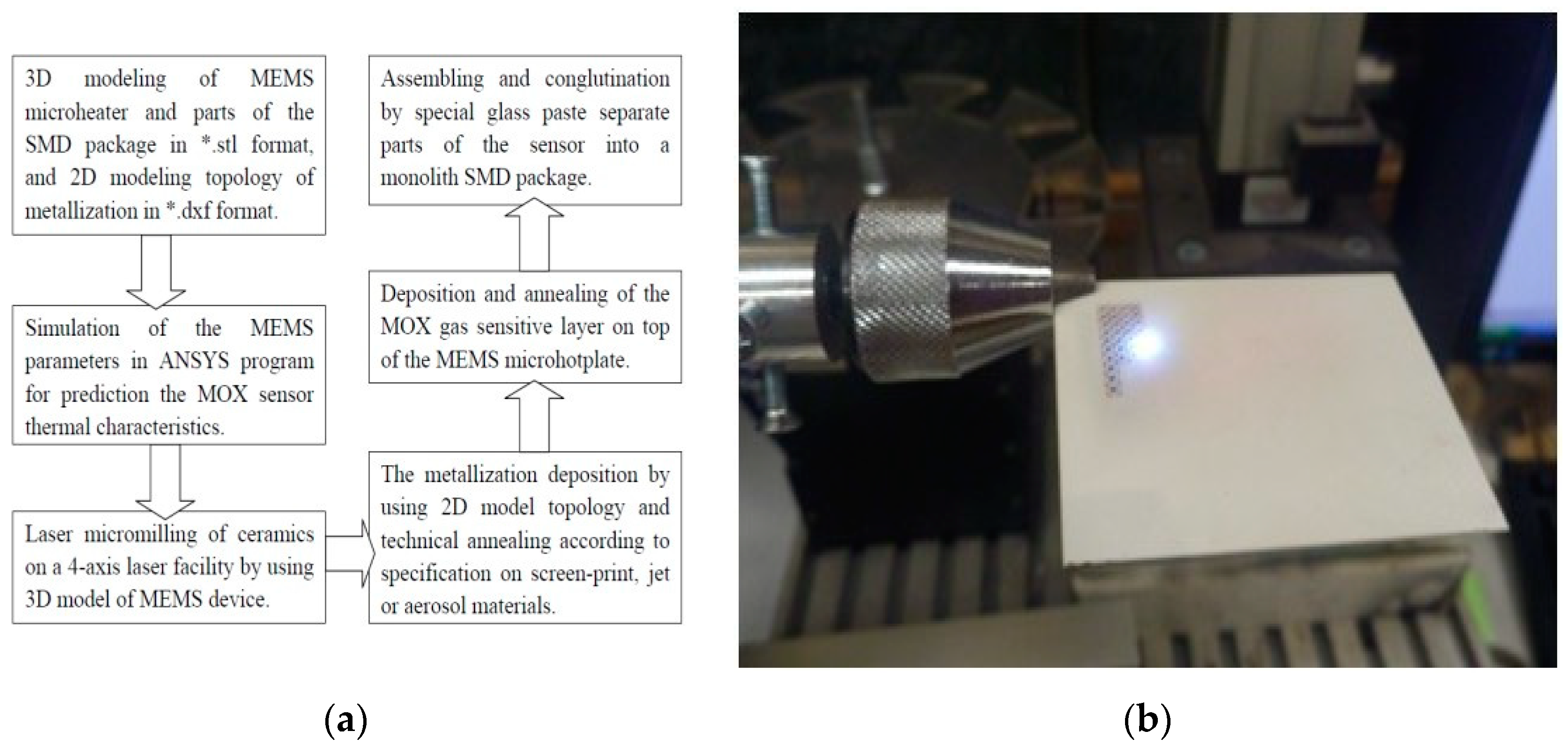
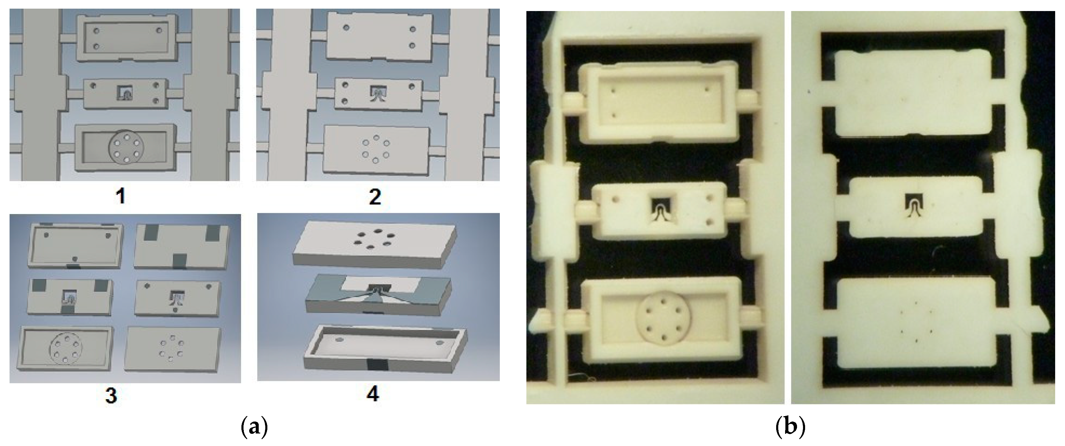
As a technology for manufacturing ceramic MEMS microhotplate and SMD packages, we used laser micromilling of monolithic Al2O3 and screen-print to form platinum metallization on top of MEMS micrphotplate. The using technological route for MEMS and SMD package fabrication present on Figure 1a. Photo of Al2O3 substrate during micromilling by 4-axis CNC fiber laser tool are present on Figure 1b. The bottom and top view of 3D model of microhotplate and parts of SMD package are shown on the Figure 2a, and of bottom and top views on 250 µm thick Al2O3 substrate are shown on the Figure 2b.
The equipment involved in the described technology does not need clean rooms and is widely represented on the market. The software for technology is simple and accessible at the student level. The only specialized product of the proposed technology is the adaptation of machine vision to obtain the minimum possible size of the MEMS structure of the microheater and the deposition of the MOX gas sensitive layer and platinum metallization, as well as the translation program of the 3D models of MEMS microhotplate and 2D topology of metallization to a 4-axis laser micromilling facilities for automatic production.
3. Result and Discussion
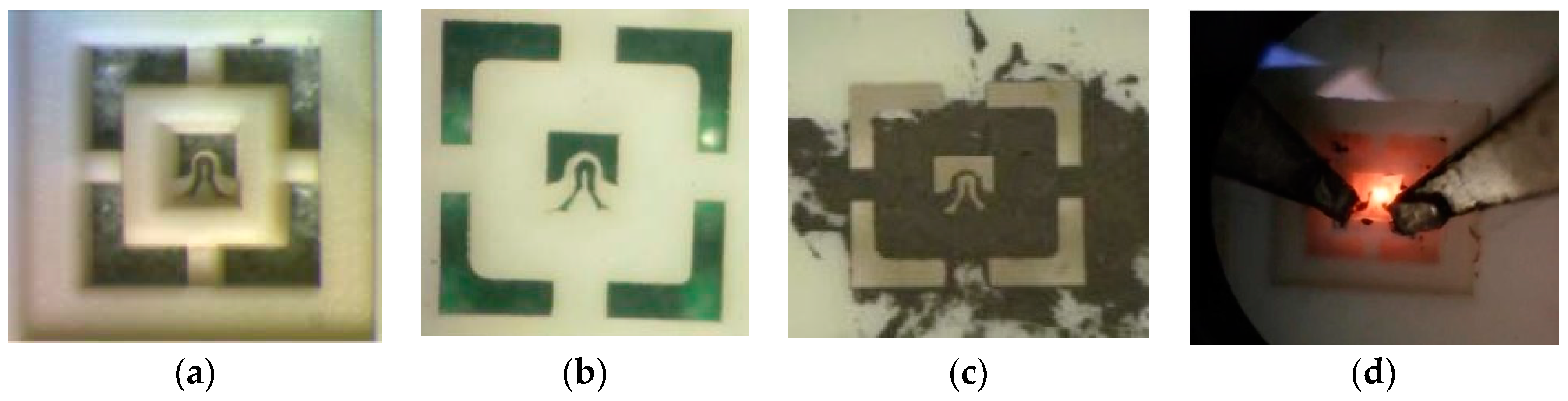
Using present approach, we fabricated the MEMS microhotplate, whose Pt track width was 30 µm and a thickness of 20 µm (see Figure 3 and Figure 4). The power consumption of MEMS microhotplate at 450 °C was approximately 250 mW (350 mW at ≈ 600 °C—“burning” platinum temperature, present on Figure 3d). Current results gives the prospect that manufacture MOX sensor in the SMD SOT-23 package type (max dissipating power by form-factor of package SOT-23 is 350 mW [10] in plastic—material with a thermal conductivity lower than Al2O3) for surface mounting in a tape is available by using described technology.
4. Conclusions
We demonstrated that the application of laser micromilling technology for the fabrication of sensing MEMS devices is very prospective and assures important advantages in comparison with traditional expensive clean room technologies. These advantages are related first of all with a very considerable enlargement of the range of working temperatures (up to 800 °C) and of the range of technological treatment temperature of the sensor (up to almost 1000 °C compare with maximum 720 °C for silicon technology). This enlargement of temperature range results in the possibility to detect gases, not detectable with silicon based devices and to improve significantly the selectivity of gas sensors using temperature modulation regime of operation [11]. Another important result is the possibility to fabricate sensors operating under harsh environmental conditions including industrial and natural catastrophes using ceramic material stable for high temperatures and aggressive agents.
Author Contributions
N.S. conceived and designed the experiments; N.Z. and K.O. performed the experiments fabrication and measurements; A.I. analyzed the data; N.V. made SEM photos; B.P. wrote the paper.
Acknowledgments
This work was supported by the Ministry Education and Science Russian Federation (Grant No. 14.584.21.0030 from 22 November 2017, unique identifier RFMEFI58417X0030) in frame of joint Russian-Korean project.
Conflicts of Interest
The authors declare no conflict of interest.
References
- Simon, I.; Bârsan, N.; Bauer, M.; Weimar, U. Micromachined metal oxide gas sensors: Opportunities to improve sensor performance. Sens. Actuators B Chem. 2001, 73, 1–26. [Google Scholar] [CrossRef]
- Available online: https://www.sensirion.com/en/environmental-sensors/gas-sensors/ (accessed on 20 July 2018).
- Available online: http://ams.com/eng/Products/Environmental-Sensors/Gas-Sensors/AS-MLV-P2 (accessed on 20 July 2018).
- Available online: https://www.bosch-sensortec.com/bst/products/all_products/bme680 (accessed on 20 July 2018).
- Available online: https://www.sgxsensortech.com/content/uploads/2014/08/1107_Datasheet-MiCS-2714.pdf (accessed on 20 July 2018).
- Available online: http://www.figarosensor.com/products/entry/tgs8100.html (accessed on 20 July 2018).
- Oblov, K.; Ivanova, A.; Soloviev, S.; Samotaev, N.; Lipilin, A.; Vasiliev, A.; Sokolov, A. Fabrication of microhotplates based on laser micromachining of zirconium oxide. Phys. Procedia 2015, 72, 485–489. [Google Scholar] [CrossRef]
- Vasiliev, A.A.; Pavelko, R.G.; Gogish-Klushin, S.Y.; Kharitonov, D.Y.; Gogish-Klushina, O.S.; Sokolov, A.V.; Pisliakov, A.V.; Samotaev, N.N. Alumina MEMS platform for impulse semiconductor and IR optic gas sensors. Sens. Actuators B Chem. 2008, 132, 216–223. [Google Scholar] [CrossRef]
- Vasiliev, A.A.; Pisliakov, A.V.; Sokolov, A.V.; Samotaev, N.N.; Soloviev, S.A.; Oblov, K.; Guarnieri, V.; Lorenzelli, L.; Brunelli, J.; Maglione, A.; et al. Non-silicon MEMS platforms for gas sensors. Sens. Actuators B Chem. 2016, 224, 700–713. [Google Scholar] [CrossRef]
- Available online: https://www.diodes.com/assets/Datasheets/ds18001.pdf (accessed on 20 July 2018).
- Samotaev, N.N.; Vasiliev, A.A.; Podlepetsky, B.I.; Sokolov, A.V.; Pisliakov, A.V. The mechanism of the formation of selective response of semiconductor gas sensor in mixture of CH4/H2/CO with air. Sens. Actuators B Chem. 2007, 127, 242–247. [Google Scholar] [CrossRef]
Figure 1.
(a)The technological route of manufacturing MEMS device in SMD package; (b) Photo of micromilling by 4-axis CNC 1064 µm wavelength fiber laser tool 250 µm thick Al2O3 substrate during fabrication microhotplates for MOX gas sensor.
Figure 1.
(a)The technological route of manufacturing MEMS device in SMD package; (b) Photo of micromilling by 4-axis CNC 1064 µm wavelength fiber laser tool 250 µm thick Al2O3 substrate during fabrication microhotplates for MOX gas sensor.

Figure 2.
(a) 1—Bottom and 2—Top view of 3D model of microhotplate and parts of SMD package as a task for laser micromilling. 3—Scheme of metallization topology in 3D model. 4—Scheme of assembling MEMS microhotplate in SMD package; (b) Photos of bottom (left) and top (right) views on 250 µm thick Al2O3 substrate with parts of SMD MOX gas sensor in SOT-23 package after laser micromilling. External dimension of SOT-23 package is 1.6 × 2.8 mm.

Figure 3.
(a)—Bottom view of MEMS microhotplate after laser micro milling. Chip size 1 × 1 mm by border of internal frame; (b)—Top view of MEMS. Internal window size 0.3 × 0.3 mm. Central track width is 30 µm; (c) Microheater track width 30 µm under cower Pt paste; (d) Testing MEMS microhotplate under voltage load (pins). Hot area at ≈ 600 °C.

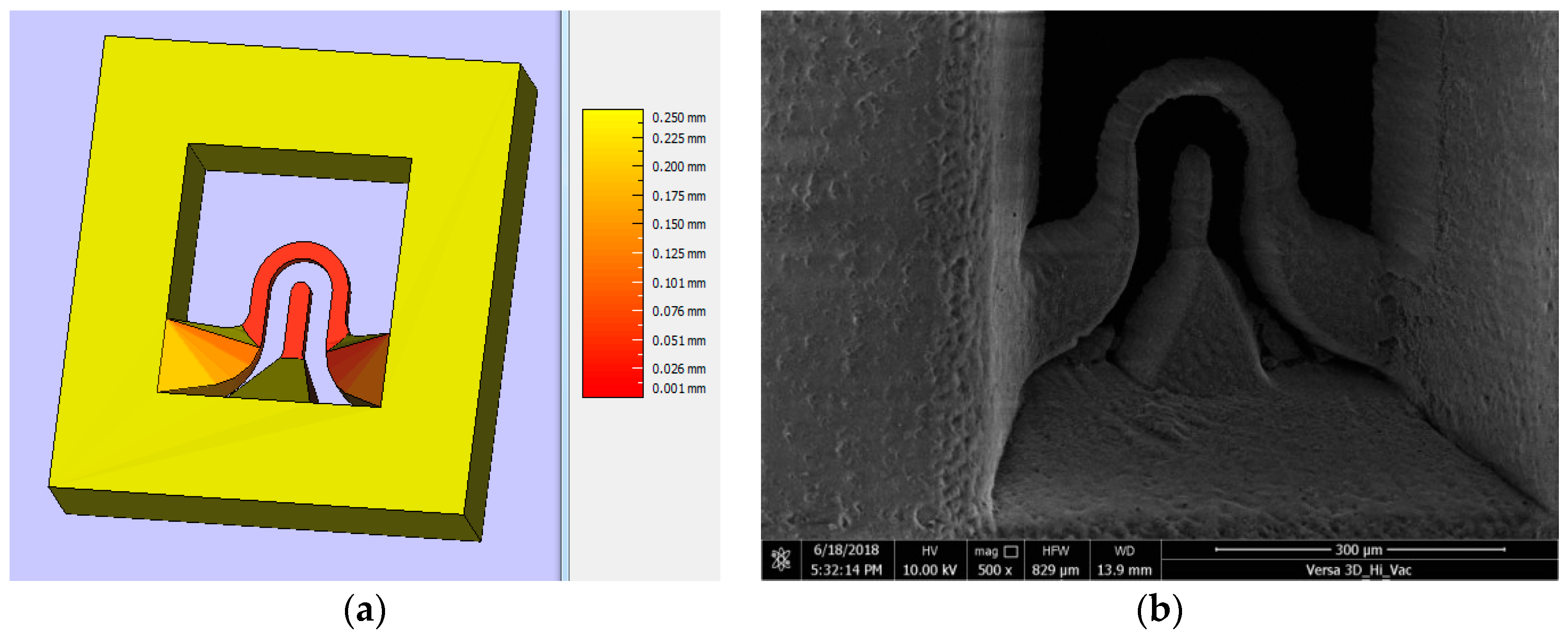
Figure 4.
(a) 3D model of MEMS microhotplate in *.stl format (Print Screen in Autodesk Inventor CAD program); (b) SEM photo MEMS microhotplate immediately after laser micromilling of 250 µm thick Al2O3 substrate using 3D model of MEMS microhotplate in *.stl format as a source CNC-code.
Figure 4.
(a) 3D model of MEMS microhotplate in *.stl format (Print Screen in Autodesk Inventor CAD program); (b) SEM photo MEMS microhotplate immediately after laser micromilling of 250 µm thick Al2O3 substrate using 3D model of MEMS microhotplate in *.stl format as a source CNC-code.

Publisher’s Note: MDPI stays neutral with regard to jurisdictional claims in published maps and institutional affiliations. |
© 2018 by the authors. Licensee MDPI, Basel, Switzerland. This article is an open access article distributed under the terms and conditions of the Creative Commons Attribution (CC BY) license (https://creativecommons.org/licenses/by/4.0/).
Share and Cite
MDPI and ACS Style
Samotaev, N.; Oblov, K.; Ivanova, A.; Podlepetsky, B.; Volkov, N.; Zibilyuk, N. Technology for SMD Packaging MOX Gas Sensors. Proceedings 2018, 2, 934. https://0-doi-org.brum.beds.ac.uk/10.3390/proceedings2130934
AMA Style
Samotaev N, Oblov K, Ivanova A, Podlepetsky B, Volkov N, Zibilyuk N. Technology for SMD Packaging MOX Gas Sensors. Proceedings. 2018; 2(13):934. https://0-doi-org.brum.beds.ac.uk/10.3390/proceedings2130934
Chicago/Turabian StyleSamotaev, Nikolay, Konstantin Oblov, Anastasia Ivanova, Boris Podlepetsky, Nikolay Volkov, and Nazar Zibilyuk. 2018. "Technology for SMD Packaging MOX Gas Sensors" Proceedings 2, no. 13: 934. https://0-doi-org.brum.beds.ac.uk/10.3390/proceedings2130934