
An Ultra-Energy-Efficient Reversible Quantum-Dot Cellular Automata 8:1 Multiplexer Circuit

1
Division of Electronic and Electrical Engineering, School of Engineering, Faculty of Engineering and Technology, Liverpool John Moores University, Liverpool L3 2ET, UK
2
Department of Computer Science, Electronics and Electrical Engineering, Faculty of Science and Engineering, University of Chester, Chester CH1 4BJ, UK
*
Author to whom correspondence should be addressed.
Quantum Rep. 2024, 6(1), 41-57; https://0-doi-org.brum.beds.ac.uk/10.3390/quantum6010004
Submission received: 24 November 2023
/
Revised: 8 January 2024
/
Accepted: 12 January 2024
/
Published: 16 January 2024
(This article belongs to the Special Issue New Reports on Quantum Mechanics: Discoveries, Promising Trends, and Technological Innovations)
Abstract
:Energy efficiency considerations in terms of reduced power dissipation are a significant issue in the design of digital circuits for very large-scale integration (VLSI) systems. Quantum-dot cellular automata (QCA) is an emerging ultralow power dissipation approach, distinct from traditional, complementary metal-oxide semiconductor (CMOS) technology, for building digital computing circuits. Developing fully reversible QCA circuits has the potential to significantly reduce energy dissipation. Multiplexers are fundamental elements in the construction of useful digital circuits. In this paper, a novel, multilayer, fully reversible QCA 8:1 multiplexer circuit with ultralow energy dissipation is introduced. The power dissipation of the proposed multiplexer is simulated using the QCADesigner-E version 2.2 tool, describing the microscopic physical mechanisms underlying the QCA operation. The results show that the proposed reversible QCA 8:1 multiplexer consumes 89% less energy than the most energy-efficient 8:1 multiplexer circuit previously presented in the literature.
1. Introduction
Advancements in complementary metal-oxide semiconductor (CMOS) technology have led to growing concern about its associated shortcomings, including subthreshold voltage and gate leakage current [1]. Additionally, the escalating demand for increasing the number of devices in CMOS systems on a chip (SoC), already at a count of billions, exacerbates the issue of excessive power dissipation [2]. Quantum-dot cellular automata (QCA) is a promising computing concept in which cells containing four quantum dots are used to perform computations at the nanoscale level. The QCA concept is based on a transistor-less paradigm in which binary information is encoded via the electron charge location in the four quantum dots of a QCA cell in antipodal configurations [3]. QCA offers several advantages over conventional semiconductor-based technologies such as CMOS, including highly reduced power consumption, the potential for high-speed operation, and the ability to create ‘nanochip’ integrated circuits with a high QCA cell density. Designing QCA digital circuits using a reversible design technique can yield enhanced circuits with ultralow-energy dissipation [4]. Theoretically, reversible computation operations, which maintain reversibility from the synthesis of a circuit to its physical layout, can mitigate information loss and require zero accompanying energy dissipation [5].
The implementation of the QCA paradigm has been proposed utilising many technologies, such as solid-state metallic island dots, magnetic implementations, and molecular electronic methods [6,7,8,9], with particularly promising atomic silicon quantum dot work employing a silicon dangling bond on a hydrogen-terminated silicon surface [10]. Molecular field-coupled nanocomputing (FCN) is anticipated to offer QCA circuits with extremely high frequencies and high device density [11,12]. The electrostatic molecular characteristics have a significant impact on the interaction and may affect the operation of the QCA circuits. The literature introduced three molecular species: neutral, oxidised, and zwitterionic [13].
The neutral molecule exhibits the lowest crosstalk effect and streamlines the inversion process, which may be achieved with a single-branch interaction. Nevertheless, the neutral molecule lacks net positive charges on the logical dots. As a result, changing its switching characteristics is necessary to reconfigure the neutral molecule. The oxidised molecule has an associated external electric field that has the capacity to displace the entire positive charge, hence enhancing the clocking functionality. However, the molecules that have undergone oxidation exhibit the most severe interference, making it challenging to create even basic circuits. Additionally, the oxidised molecular cell exhibits a strong repulsive force, rendering the inversion process impossible with a single-branch interaction. The zwitterionic molecule exhibits an intermediary behaviour that lies between that of neutral molecules and oxidised molecules. The presence of a positive net charge on the logic dots allows for the molecular cell to be reset by adding a negative clock field, while the molecule’s neutrality helps to minimise crosstalk. It is crucial to observe that the location of the counterion has a significant impact on the behaviour of the device. When the counterion is in close proximity to the logical dots, the zwitterionic molecule mimics the behaviour of a neutral molecule. However, when the counterion is far away, it exhibits similarities to oxidised molecules.
In very large-scale integration (VLSI) systems, a multiplexer is a digital circuit that selects one input data line and forwards the selected data to a single output line based on a set of control signals. Multiplexers are pervasive in digital electronics and are used for data routing and selection. QCA 8:1 multiplexer circuits have received significant attention in previous research due to their essential role in constructing digital circuits for computing systems. Energy efficiency is a fundamental consideration in the development of computer circuits. Several previous studies have proposed various configurations for reversible QCA 8:1 multiplexer circuits with the aim of reducing energy dissipation. These studies addressed reversibility only at the synthesis level and neglected reversibility at the layout level, i.e., the physical ‘instantiation’ of the circuit. However, maintaining reversibility at the physical level is the only way to achieve significant energy reductions in reversible computing [4]. Therefore, in this study, we present an innovative multilayer design for a QCA 8:1 multiplexer circuit that is both logically and physically reversible. The design preserves reversibility throughout the entire circuit design process, from the synthesis level down to the layout level. This design technique mitigates the loss of information and consequently produces circuits that have near-zero energy dissipation. The QCADesigner-E version 2.2 software tool [14], which provides a microscopic quantum mechanical description of QCA cell behaviour with a Hartree treatment of cell–cell electrostatic interactions, is employed to simulate the performance and energy dissipation of the design.
The remainder of this paper is organised as follows: Section 2 presents an analysis of the process of energy dissipation in QCA technology. In Section 3, the fully reversible design concept is explained. In Section 4, the hierarchical design process for the proposed fully reversible QCA 8:1 multiplexer circuit is presented. Simulation results are reported and discussed in Section 5, and the conclusions of the current study are provided in Section 6.
2. Energy Dissipation Analysis of QCA Cells
A QCA cell starts each clock cycle in a depolarised state. Energy needs to be supplied by the clock to reach a polarised state. Most of this energy goes back to the clock and other cells when the cell depolarises again at the end of the clock cycle. However, some energy is dissipated into the environment. To study the energy loss of QCA cells in detail, a microscopic quantum mechanical model of QCA cell behaviour needs to be used, as employed in previous studies [14,15,16,17].
Presently, there exist two tools, namely QCADesigner-E [14] and QCAPro [16], that enable the modelling of energy dissipation in QCA circuits. The QCAPro simulation tool, developed in 2009, cannot provide precise estimates due to the assumption of a perfect clock slope. Consequently, it permits only the determination of an upper limit for energy dissipation. On the other hand, QCADesigner-E can compute the actual energy dissipation values. It calculates the energy transmission to and from the clock (), the neighbouring cells (), and the environment () by calculating the corresponding integral equations for these quantities. The QCADesigner-E software is an enhancement of the well-known QCA technology computer-aided design (TCAD) package, QCADesigner [18].
QCADesigner incorporates a coherence vector simulation engine (CVSE). The CVSE utilises an advanced quantum mechanical density matrix-based treatment, as described in the literature [14,15,16], to simulate the behaviour of QCA cells, including energy dissipation. It uses a computational method to perform a transient analysis for the quantum mechanical density matrix-based microscopic description of the intracell dynamics, while the cell–cell electrostatic interactions are incorporated within the Hartree approximation [18]. During each iteration, the CVSE calculates updated values for the coherence vector components, given the time-dependent tunnelling energy determined by the clock. The coherence vector formalism uses the Pauli spin matrices to form the basis for the coherence vector. By solving the matrix differential equations that reflect the evolution of the quantum mechanical density matrix, the coherence vector is determined. This is accomplished using an iterative fixed-timestep technique [14]. The timestep must be sufficiently small to minimise simulation errors and obtain accurate outcomes. The technological specifications for the physical implementation of the circuits proposed in this study are outlined in Table 1.
Going into further detail, the microscopic quantum mechanical model represents the state of a QCA cell using two three-dimensional vectors: the coherence vector and the energy vector. The coherence vector represents the current state of the cell, where the parameter corresponds to the negative of its polarisation [14]. The energy vector , where is the reduced Planck constant, describes the steady state of the cell, which indicates how the cell will behave in the future based on its current tunnelling behaviour () and the Coulomb force exerted by neighbouring cells (given by when expressed as a potential energy).
The kink energy between two cells i and j measures the energy cost of those cells having opposite polarisations. The polarisation of a cell is determined by the positions of the two excess electrons in the four quantum dots that form the cell [3]. The polarisation of a cell can be influenced by the polarisation of its neighbouring cells through Coulomb interactions, as follows:
To calculate the current energy of a QCA cell, the formula is used, where is the trace operator, is the Hamiltonian of the cell, and is the density matrix of the cell. The Hamiltonian contains terms representing the Coulomb interaction between electrons in the current cell and its nearest neighbours and the tunnelling between the quantum dots within the cell. The density matrix represents the statistical state of the cell, such as the probability of finding an electron in a certain quantum dot. By taking the expectation value of with respect to , we can obtain the average energy of the cell at any given time. By exploiting the linearity of the operator and using , we can calculate the energy dissipation of a QCA cell as a function of time:
where the function denotes the current energy of the cell at time and is essentially given by the scalar product of the two energy vectors at that point in time.
To calculate the instantaneous power P of a QCA cell, the following expression can be used:
Consequently, the total energy dissipation of a QCA cell during a complete clock cycle, with a period is given as the integral of over one cycle:
The integrand of Equation (3) is the scalar product of the derivative of the energy vector and the coherence vector of the cell. This expression describes the amounts of energy transmitted within the clock and the neighbouring cells during a clock cycle [14,15,16], which can be calculated as follows:
Moreover, it captures the energy transferred to the environment within a clock cycle [14,15,16]. represents the energy dissipated by a QCA cell during a clock cycle and can be calculated as follows:
where is a technology-dependent relaxation time parameter and denotes the thermal ratio and can be calculated as follows:
As indicated in [15,19], the system relaxes towards the thermal steady-state, and to ensure the precision of the calculations, energy conservation must hold numerically, meaning that the total energy must be zero, i.e.,
The default values of QCADesigner-E version 2.2 [14], as displayed in Table 2, were utilised for the time interval of each iteration step (Tstep) and other simulation parameters. Previous research studies [14,20,21,22,23] indicate that when the default simulation parameters are used, this tool yields precise outcomes with numerical energy conservation errors of less than 5%.
3. Fully Reversible Design Concept
Conventional computing techniques commonly involve irreversible operations, resulting in the deletion of some of the input bits of data during the computational process. This information loss is accompanied by some dissipation of energy, kBTln2 per bit erased, where kB is the Boltzmann constant, and T is the temperature [24], as a consequence of the second law of thermodynamics. When reversible logic operations are used instead of typically irreversible computations, a one-to-one correspondence is maintained between the input and output signals. Thus, from the outset, unlike irreversible computations, reversible operations have no information loss with an accompanying dissipation of energy into the environment. However, substantially reducing energy usage in reversible computing requires preserving reversibility down to the physical level [4]. Therefore, in both the design synthesis and architecture layout, the implementation of the circuit must be reversible to avoid energy dissipation.
In recent years, scholars have grown increasingly interested in investigating the development of reversible QCA circuits [25,26,27,28]. Nevertheless, their designs focus on circuit reversibility at the synthesis level, neglecting the potential loss of information arising from irreversibility at the physical layout level. In 2020, a novel reversible design technique was proposed for the synthesis and layout of a combinational QCA half-adder circuit [23]. This innovative approach emphasises preserving reversibility throughout the entire circuit design process at all levels. The findings of this simulation and modelling research indicate that combinational QCA designs that maintain reversibility down to the layout level generate QCA circuits that dissipate less energy than the Landauer theoretical limit of kBTln2. However, the authors neglected the need for data synchronisation, which can affect the precision of a QCA digital circuit’s computations. The current authors have tackled this important time-synchronisation issue by employing a circuit architecture that is intrinsically more symmetrical [13]. The novel fully reversible time-synchronised design technique was subsequently used to investigate, via simulation, more complex combinational QCA logic circuit designs [20,22] as well as sequential QCA circuits, which have internal feedback loops by nature [21].
The process of designing QCA circuits typically entails the use of two fundamental types of logic gates: QCA majority gates and QCA inverters. The inclusion of these two types of gates is crucial in QCA circuit design because their combination allows for the implementation of Boolean functions. The ability to construct complex logic functions using combinations of majority gates and inverters makes QCA a promising technology for future computing architectures, particularly in areas where minimising power consumption and maximising speed are critical.
The QCA inverter is inherently reversible because it possesses a one-to-one relationship between the input and output signals. Two distinct configurations for QCA inverters are described in the literature: the single-branch inverter shown in Figure 1a and the double-branch inverter depicted in Figure 1b. The choice between single-branch and double-branch inverters in QCA circuits depends on numerous factors, such as size constraints, the desired computational speed, sensitivity to noise, stability needs, the complexity of the overall system, and the technology used [13].
Conversely, the conventional QCA majority gate is irreversible and features three inputs and one output, as illustrated in Figure 2. Figure 2a shows a schematic depiction of the logical design, while Figure 2b shows the cell layout of the conventional three-input QCA majority gate. Energy dissipation in QCA circuits is primarily attributed to the use of conventional irreversible majority gates [29]. The three-input majority gate can be configured as either an ‘AND’ gate or an ‘OR’ gate by assigning a binary value of ‘0’ or ‘1’ to one of its inputs. Torres et al. [23] have demonstrated that fully reversible 2-bit recycling QCA ‘AND’ and ‘OR’ gates can enable the construction of computing circuits with an energy loss lower than kBTln2 joules. This is because it guarantees a one-to-one relationship between its initial and final states.
In this paper, a novel fully reversible QCA 8:1 multiplexer circuit with ultralow energy consumption is designed by employing the fully reversible time-synchronised QCA design approach and is subsequently simulated. The proposed novel design approach uses fully reversible ‘AND’ and ‘OR’ gates as its fundamental components. Moreover, the single-branch inverter is used due to its simplicity, space efficiency, and fast operations. However, the single-branch inverter operates exclusively with neutral molecules or with well-engineered zwitterionic molecules that have relatively low profiles [13].
The VLSI hierarchical design process for designing a fully reversible 8:1 multiplexer in QCA may be broken down into the following stages:
- Designing a QCA three-input-three-output majority gate. Subsequently, utilise it to produce reversible ‘AND’ and reversible ‘OR’ gates.
- Reversibly designing a QCA 2:1 multiplexer using two reversible AND gates, one reversible OR gate, and one single-branch inverter.
- Reversibly designing a QCA 4:1 multiplexer containing three reversible QCA 2:1 multiplexers.
- Reversibly designing a QCA 8:1 multiplexer containing two reversible QCA 4:1 multiplexers and an additional single reversible QCA 2:1 multiplexer.
Synchronisation of the data flows in logic circuits is crucial for ensuring accurate data transmission and functioning. For QCA circuits, an external clock is applied to modify the strength of the tunnelling barriers between QCA cells, allowing control of the timing. Numerous timing and clocking schemes have been suggested to govern the transfer of information in QCA circuits [30,31,32]. Data flow synchronisation in our proposed circuit is achieved by utilising the unified, standard, and efficient (USE) timing approach [32]. The USE timing approach possesses a high degree of flexibility, allowing it to effectively meet the requirements of QCA circuit design. These requirements include the incorporation of feedback channels with varying loop sizes, the establishment of standardised cell libraries, and the promotion of simplified routing. The USE clocking system consists of four time zones labelled from 1 to 4. Each time zone consists of a cluster of five-by-five QCA cells and represents a distinct time period. The combination of these four time zones constitutes a complete clock cycle. The reader is referred to the previous papers [11,12,13,14] for further details.
One of the most challenging issues encountered when designing digital logic circuits pertains to the handling of wire junctions. In this study, the wire-crossing problem is solved using the multilayer technique developed by Bajec and Pecar [33]. This technique is used to design a reversible QCA 8:1 multiplexer circuit with three distinct layers to solve the wire junction issue.
4. Design Process of the Proposed Fully Reversible QCA 8:1 Multiplexer
The primary goal of this study is to create a reversible QCA 8:1 multiplexer circuit that has exceptionally low energy consumption. Hence, a fully reversible design methodology that inherently overcomes the information loss issue is utilised. The design process involves several stages of development and represents an application of hierarchical design.
4.1. Reversible Fundamental Logic Gates
The three-input majority gate is the fundamental logic gate used in QCA circuits. It determines the majority value among its three inputs, i.e., it exhibits majority voting behaviour. It is mathematically represented in Equation (11).
The three-input majority gate is programmed to produce an ‘AND’ gate or an ‘OR’ gate by setting a binary value of ‘0’ or ‘1’ to one of its inputs. Thus, fixing input C in Equation (11) to the value of ‘0’ can produce an ‘AND’ gate with the Boolean expression given in Equation (12).
Also, fixing input C in Equation (11) to the value of ‘1’ results in the generation of an ‘OR’ gate with the Boolean expression given in Equation (13).
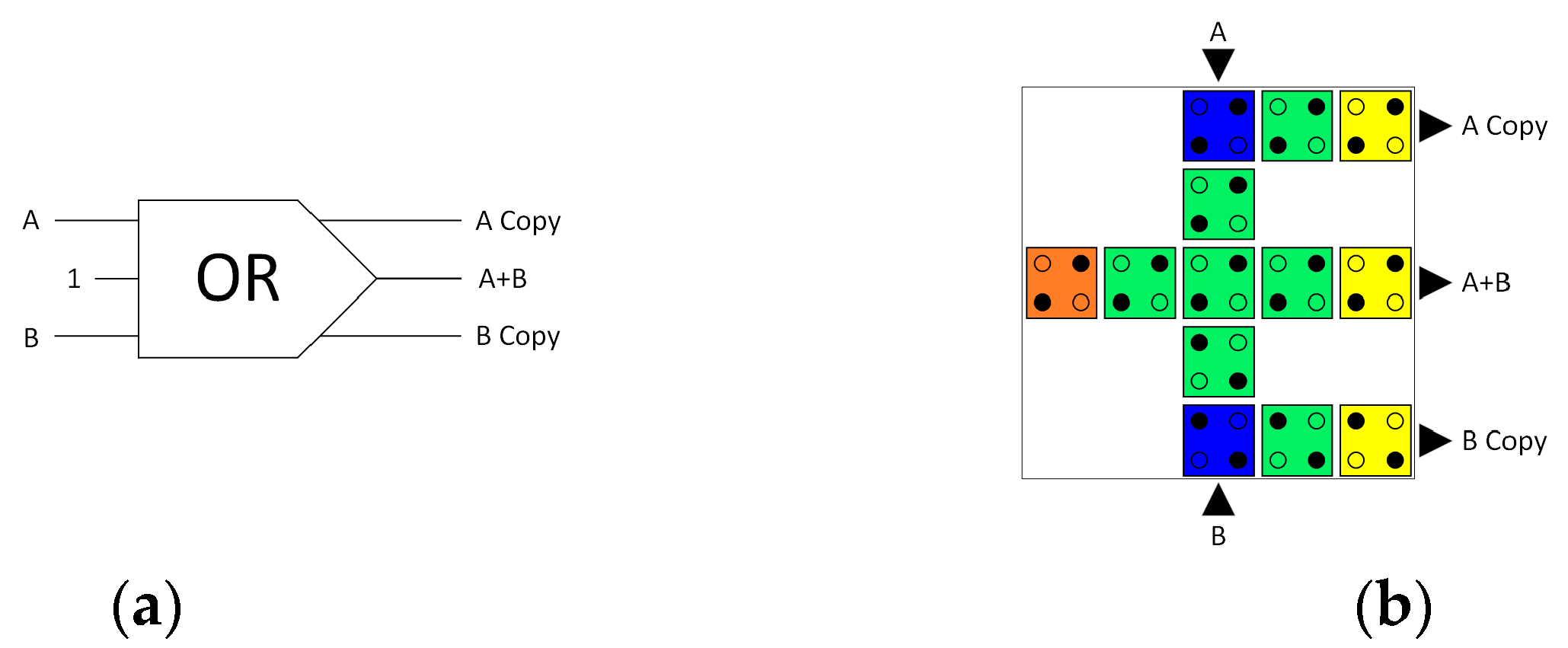
The majority gate is widely recognised as the principal contributing factor to energy dissipation in QCA circuits [29]. The conventional majority gate in QCA is inherently irreversible because it has three input pins and only a single output pin. As a result of the information loss corresponding to the two ’missing’ output pins, the second law of thermodynamics demands that heat be dissipated into the environment. Consequently, our initial focus was on developing a majority gate with three inputs and three outputs, as demonstrated in Figure 3. This three-input-three-output majority gate replicates the data for two inputs, labelled A and B, into two outputs, labelled A Copy and B Copy, resulting in an overall situation with equal numbers of binary inputs and outputs. Figure 3a illustrates a schematic depiction of the logical design, while Figure 3b shows the cell layout design of the QCA three-input-three-output majority gate.
Subsequently, we utilised this majority gate to generate fully reversible ‘AND’ and ‘OR’ gates that recycle two input bits. The recycling of two input bits can make the QCA ‘AND’ gate and ‘OR’ gate reversible [23]. The functionality of the three-input-three-output majority gate is determined by the input labelled C.
Assigning input C to ‘0′ can produce a reversible ‘AND’ gate, as shown in Figure 4. Figure 4a illustrates a schematic depiction of the logical design, while Figure 4b shows the cell layout design of the fully reversible QCA AND gate.
On the other hand, assigning input C to ‘1′ can produce a reversible ‘OR’ gate, as shown in Figure 5. Figure 5a illustrates a schematic depiction of the logical design, while Figure 5b shows the cell layout design of the fully reversible QCA OR gate.
In this research, the fully reversible ‘AND’ and ‘OR’ gates are the main building ‘blocks’ in the development of fully reversible QCA multiplexers.
4.2. Reversible 2:1 Multiplexer
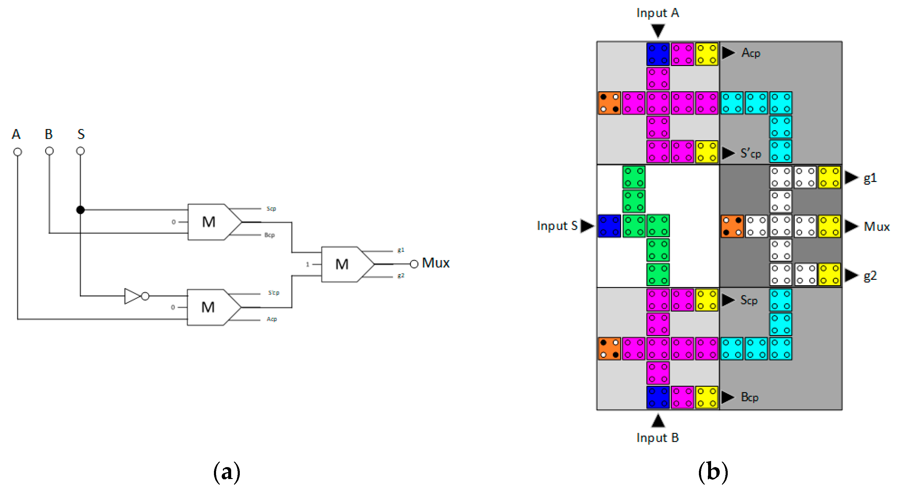
The next step of the design process for the fully reversible QCA 8:1 multiplexer circuit is the creation of a fully reversible QCA 2:1 multiplexer circuit, which serves as the central ‘organ’ of the design. This 2:1 multiplexer utilised the fully reversible ‘AND’ and ‘OR’ gates presented in Section 4.1 as the main building elements. Specifically, the reversible 2:1 multiplexer is composed of two reversible ‘AND’ gates, one reversible ‘OR’ gate, and one single-branch inverter, as shown in Figure 6. The circuit synthesis diagram is depicted in Figure 6a, and the QCA cell layout design is shown in Figure 6b. The delay of the reversible QCA 2:1 multiplexer is four clock zones, which is equal to one complete clock cycle. This design requires the use of 56 QCA cells, occupying a total area of 0.09 µm2, given the geometric parameters of the underlying technology specified in Table 1.
The Boolean expression given in Equation (14) represents the output of the proposed 2:1 multiplexer circuit in terms of the inputs, and the truth table of the circuit is presented in Table 3.
4.3. Reversible 4:1 Multiplexer
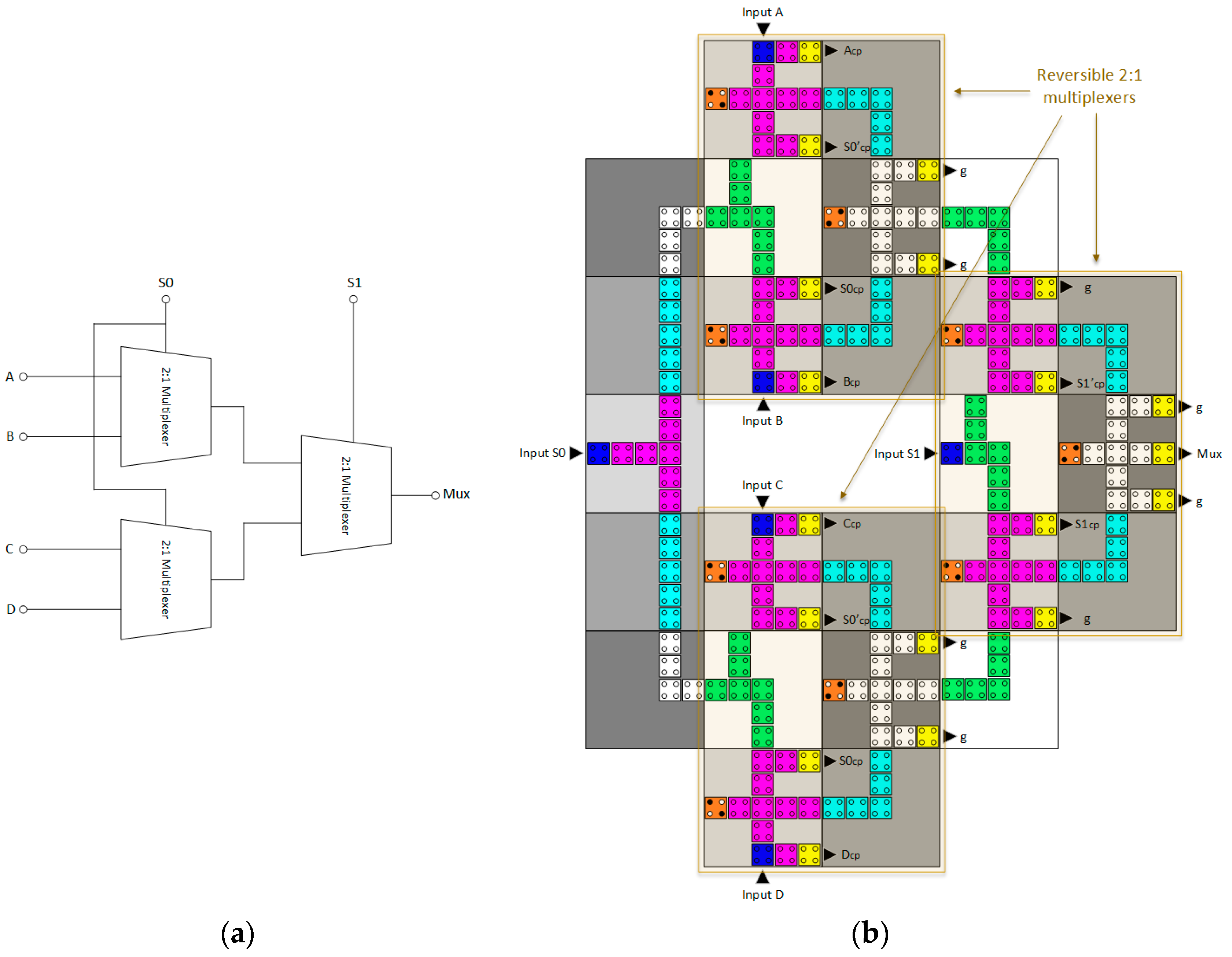
A reversible QCA 4:1 multiplexer circuit is obtained by combining three reversible QCA 2:1 multiplexer circuits, as illustrated in Figure 7. Figure 7a depicts the synthesis of the reversible QCA 4:1 multiplexer circuit, whereas Figure 7b shows the QCA cell layout design. This circuit incorporates a total of 213 QCA cells with a total area of 0.46 µm2, given the geometric technological parameters presented in Table 1. The observed delay duration is 12 clock zones, which is equivalent to three clock cycles.
Equation (12) gives the output of the proposed 4:1 multiplexer circuit in terms of the Boolean inputs, and Table 4 displays the corresponding truth table for the circuit.
4.4. Reversible 8:1 Multiplexer
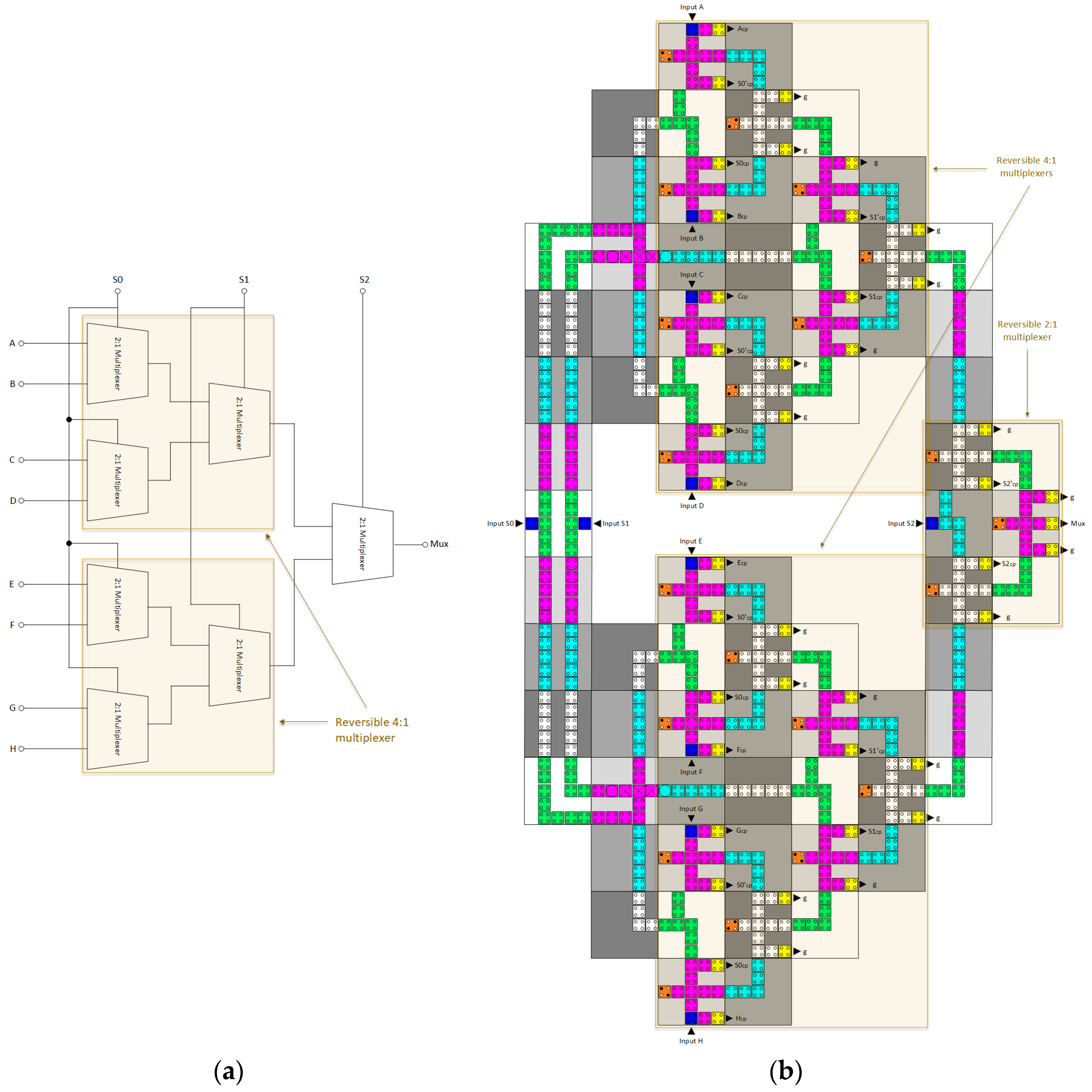
Finally, a reversible QCA 8:1 multiplexer circuit can be constructed by utilising two reversible 4:1 multiplexers and a single 2:1 reversible multiplexer, i.e., seven reversible 2:1 multiplexers in total. The hierarchical design can be divided into three distinct levels, as seen in Figure 8:
- At the first level, a set of four 2:1 multiplexers generates four output signals dependent upon the value of S0.
- At the second level, two 2:1 multiplexers produce two outputs, dependent upon the value of S1.
- At the third level, a single 2:1 multiplexer generates the final result, dependent upon the value of S2.
Figure 8a displays the synthesis process of the reversible QCA 8:1 multiplexer circuit, whereas Figure 8b displays the QCA cell layout architecture. This circuit incorporates a total of 646 QCA cells, encompassing a total area of 1.36 µm2 when the geometric technological parameters given in Table 1 are employed. The observed delay duration is 22 clock zones, which is equivalent to 5.5 clock cycles.
Equation (13) expresses the output of the proposed 8:1 multiplexer circuit in terms of the Boolean inputs, and Table 5 displays the corresponding truth table for the circuit.
5. Energy Dissipation Simulation Results and Discussion
The energy dissipation of the proposed reversible QCA 8:1 multiplexer circuit was calculated using QCADesigner-E software version 2.2 [14], applying the technology and simulation parameters presented in Table 1 and Table 2, respectively. Overall, the findings from the simulation results in Table 6 prove that the energy efficiency of QCA multiplexer circuits improves significantly when fully reversible ‘AND’ and ‘OR’ gates are used as a basic building block. This fully reversible design method, which preserves reversibility from circuit synthesis to physical layout, is able to mitigate information loss and, in theory, eliminate the energy dissipation of the circuit [5]. Table 6 highlights the remarkably low energy dissipation values of the proposed fully reversible designs. Each elementary circuit used to build the 8:1 multiplexer circuit, including the ‘AND’ gate, the ‘OR’ gate, the 2:1 multiplexer, and the 4:1 multiplexer, has an average energy dissipation that is lower than the Landauer energy threshold of 0.06 meV at a temperature of 1 K.
Table 7 displays the numbers of inverters, ‘AND’ gates, ‘OR’ gates, and QCA cells used in the construction of the proposed multiplexers. Moreover, it compares the performance among the proposed 2:1, 4:1, and 8:1 multiplexers in terms of the occupied area and delay time.
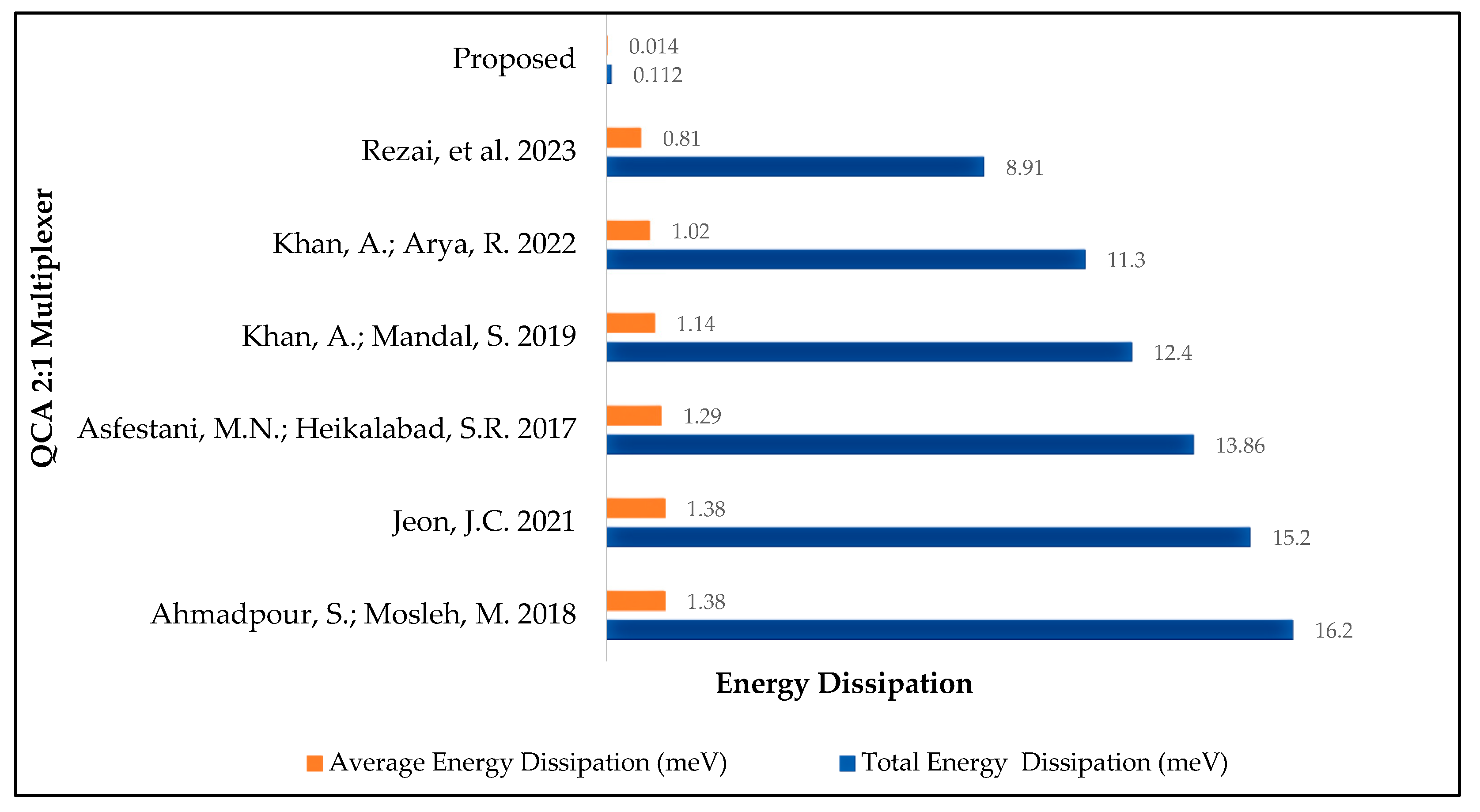
To provide a thorough energy analysis of energy consumption, we compare the proposed multiplexer circuits’ energy efficiency to that of others in the literature that use the same standard technological parameters presented in Table 1. The energy efficiency of our proposed fully reversible QCA 2:1 multiplexer circuit is compared with the energy values reported previously in the literature. The results are presented in Table 8 and Figure 9. The simulation of our fully reversible QCA 2:1 multiplexer circuit shows a 98% reduction in energy dissipation compared with the most energy-efficient QCA 2:1 multiplexer circuit design previously proposed [34].
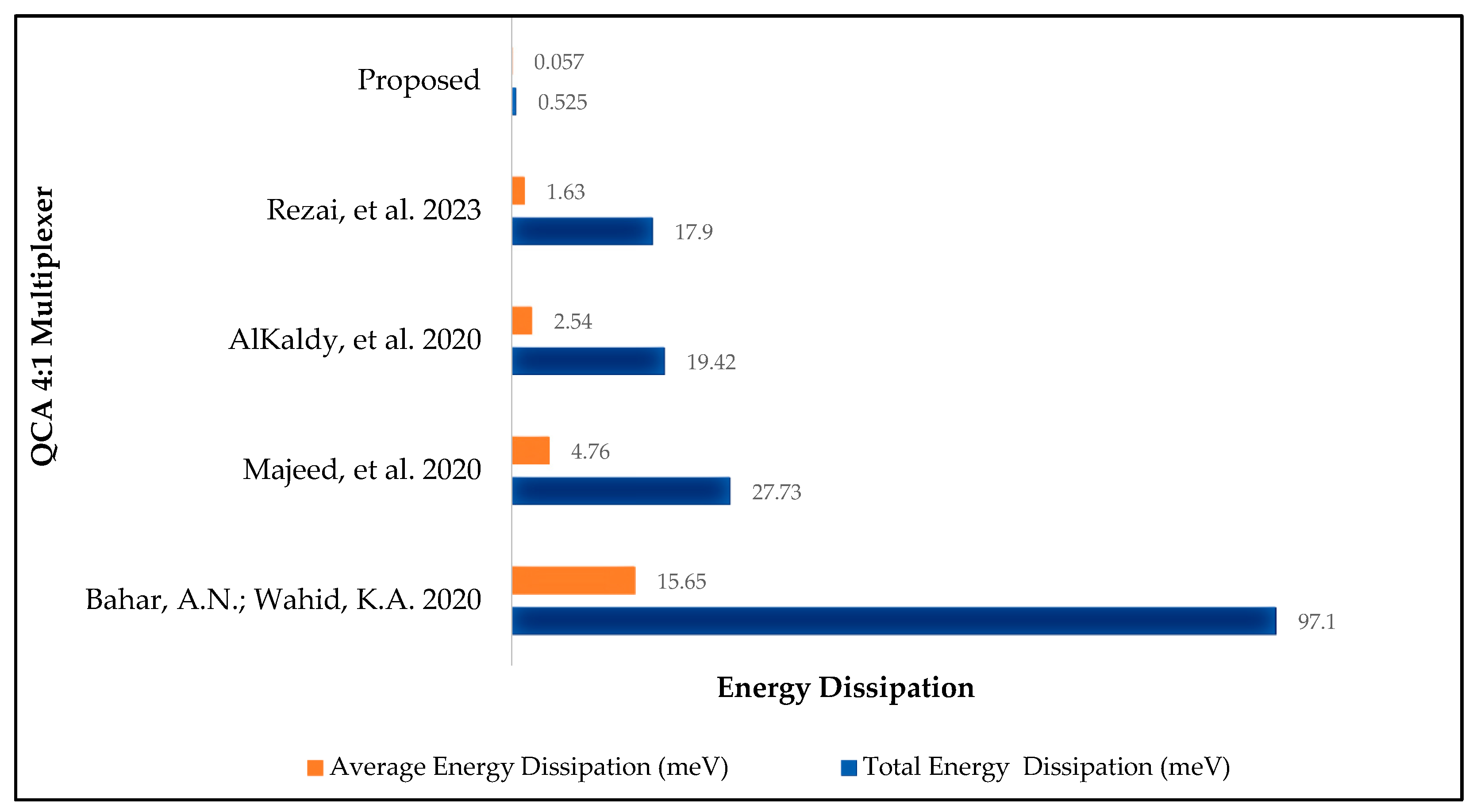
Table 9 and Figure 10 present the simulation results for our new fully reversible QCA 4:1 multiplexer circuit alongside the energy dissipation results from previous research endeavours. Our proposed fully reversible QCA 4:1 multiplexer circuit design exhibits a 97% improvement in energy efficiency compared to the most energy-efficient design previously reported [34].
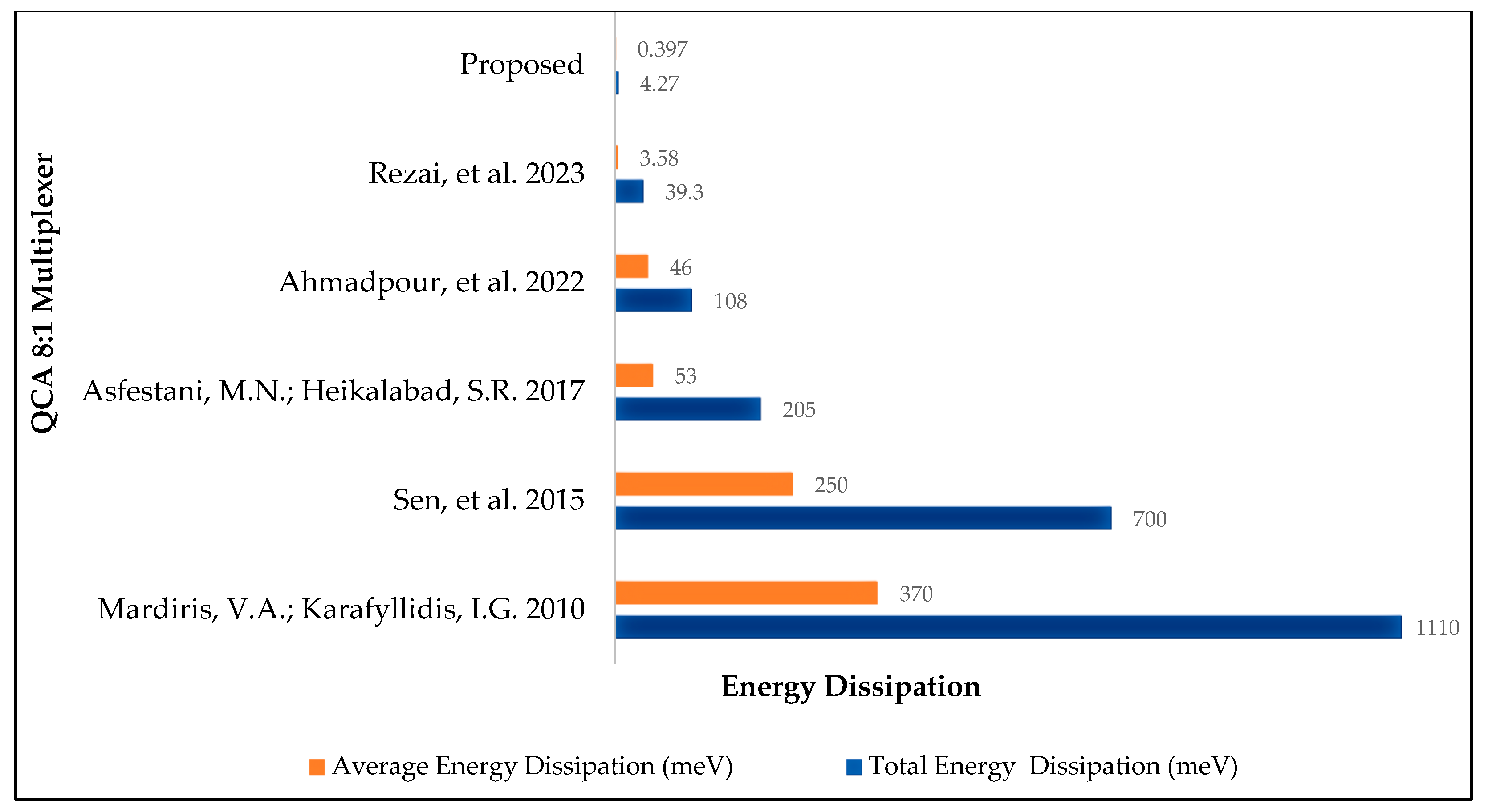
Table 10 and Figure 11 compare the energy dissipation results from different previous simulation studies with those for our novel fully reversible QCA 8:1 multiplexer circuit. The results illustrate an 89% decrease in power consumption compared to the previous most energy-efficient QCA 8:1 multiplexer circuit design [34].
6. Conclusions
Reducing power consumption is a primary concern in the design of digital computer circuits for both mobile and cloud server applications. To achieve highly energy-efficient digital computing circuits, a design approach that ensures reversibility throughout the synthesis and physical layout stages must be employed. Multiplexers are crucial basic components in many digital circuits. The primary objective of this work was to design an 8:1 multiplexer circuit that exhibits exceptionally low power consumption. First, a novel, fully reversible QCA 2:1 multiplexer circuit was devised. This fully reversible QCA 2:1 multiplexer circuit then served as the foundational building block for the development of fully reversible QCA 4:1 and 8:1 multiplexer circuits through hierarchical design techniques. The power dissipation was simulated using the QCADesigner-E software tool, which provides a microscopic description of QCA physics with a treatment of the quantum mechanical mechanisms within a cell, the electrostatic interactions between cells, and a phenomenological model of heat dissipation to the environment. The findings of this study indicate that with the simulation parameters given in Table 2, the fully reversible QCA 2:1, 4:1, and 8:1 multiplexers designed and simulated in this study dissipate 98%, 97%, and 89% less energy, respectively, than the most energy-efficient multiplexer circuits previously reported utilising the same standard technological parameters listed in Table 1.
Author Contributions
M.A., G.E. and R.S. contributed to the study’s conception and design. Circuit design, simulation, and analysis were carried out by M.A. and examined by M.A., G.E. and R.S. The first draft of the manuscript was written by M.A., then M.A., G.E. and R.S. revised the manuscript. All authors have read and agreed to the published version of the manuscript.
Funding
This research received no external funding.
Data Availability Statement
Data are contained within the article.
Conflicts of Interest
The authors declare no conflicts of interest.
References
- Sen, B.; Sengupta, A.; Dalui, M.; Sikdar, B.K. Design of Testable Universal Logic Gate Targeting Minimum Wire-Crossings in QCA Logic Circuit. In Proceedings of the 2010 13th Euromicro Conference on Digital System Design: Architectures, Methods and Tools, Lille, France, 1–3 September 2010; pp. 613–620. [Google Scholar]
- Knobloch, T.; Selberherr, S.; Grasser, T. Challenges for nanoscale CMOS logic based on two-dimensional materials. Nanomaterials 2022, 12, 3548. [Google Scholar] [CrossRef]
- Lent, C.S.; Tougaw, P.D.; Porod, W.; Bernstein, G.H. Quantum cellular automata. Nanotechnology 1993, 4, 49. [Google Scholar] [CrossRef]
- DeBenedictis, E.P.; Frank, M.P.; Ganesh, N.; Anderson, N.G. A path toward ultra-low-energy computing. In Proceedings of the 2016 IEEE International Conference on Rebooting Computing (ICRC), San Diego, CA, USA, 17–19 October 2016; pp. 1–8. [Google Scholar]
- Bennett, C.H. Logical reversibility of computation. IBM J. Res. Dev. 1973, 17, 525–532. [Google Scholar] [CrossRef]
- Orlov, A.O.; Amlani, I.; Bernstein, G.H.; Lent, C.S.; Snider, G.L. Realization of a functional cell for quantum-dot cellular automata. Science 1997, 277, 928–930. [Google Scholar] [CrossRef]
- Garlando, U.; Riente, F.; Turvani, G.; Ferrara, A.; Santoro, G.; Vacca, M.; Graziano, M. Architectural exploration of perpendicular Nano Magnetic Logic based circuits. Integration 2018, 63, 275–282. [Google Scholar] [CrossRef]
- Orlov, A.; Imre, A.; Csaba, G.; Ji, L.; Porod, W.; Bernstein, G. Magnetic quantum-dot cellular automata: Recent developments and prospects. J. Nanoelectron. Optoelectron. 2008, 3, 55–68. [Google Scholar] [CrossRef]
- Lent, C.S.; Isaksen, B.; Lieberman, M. Molecular quantum-dot cellular automata. J. Am. Chem. Soc. 2003, 125, 1056–1063. [Google Scholar] [CrossRef]
- Huff, T.; Labidi, H.; Rashidi, M.; Livadaru, L.; Dienel, T.; Achal, R.; Vine, W.; Pitters, J.; Wolkow, R.A. Binary atomic silicon logic. Nat. Electron. 2018, 1, 636–643. [Google Scholar] [CrossRef]
- Wang, Y.; Lieberman, M. Thermodynamic behavior of molecular-scale quantum-dot cellular automata (QCA) wires and logic devices. IEEE Trans. Nanotechnol. 2004, 3, 368–376. [Google Scholar] [CrossRef]
- Lent, C.S. Bypassing the transistor paradigm. Science 2000, 288, 1597–1599. [Google Scholar] [CrossRef]
- Ardesi, Y.; Beretta, G.; Vacca, M.; Piccinini, G.; Graziano, M. Impact of molecular electrostatics on field-coupled nanocomputing and quantum-dot cellular automata circuits. Electronics 2022, 11, 276. [Google Scholar] [CrossRef]
- Sill Torres, F.; Wille, R.; Niemann, P.; Drechsler, R. An Energy-Aware Model for the Logic Synthesis of Quantum-Dot Cellular Automata. IEEE Trans. Comput.-Aided Des. Integr. Circuits Syst. 2018, 37, 3031–3041. [Google Scholar] [CrossRef]
- Timler, J.; Lent, C.S. Power gain and dissipation in quantum-dot cellular automata. J. Appl. Phys. 2002, 91, 823–831. [Google Scholar] [CrossRef]
- Srivastava, S.; Sarkar, S.; Bhanja, S. Estimation of upper bound of power dissipation in QCA circuits. IEEE Trans. Nanotechnol. 2008, 8, 116–127. [Google Scholar] [CrossRef]
- Rahimi, E. Energy dissipation of quantum-dot cellular automata logic gates. Micro Nano Lett. 2016, 11, 369–371. [Google Scholar] [CrossRef]
- Walus, K.; Jullien, G.A. Design tools for an emerging SoC technology: Quantum-dot cellular automata. Proc. IEEE 2006, 94, 1225–1244. [Google Scholar] [CrossRef]
- Taucer, M.; Karim, F.; Walus, K.; Wolkow, R.A. Consequences of many-cell correlations in clocked quantum-dot cellular automata. IEEE Trans. Nanotechnol. 2015, 14, 638–647. [Google Scholar] [CrossRef]
- Alharbi, M.; Edwards, G.; Stocker, R. Design and Simulation of Reversible Time-Synchronized Quantum-Dot Cellular Automata Combinational Logic Circuits with Ultralow Energy Dissipation. Int. Trans. J. Eng. Manag. Appl. Sci. Technol. 2022, 13, 1–22. [Google Scholar] [CrossRef]
- Alharbi, M.; Edwards, G.; Stocker, R. Novel ultra-energy-efficient reversible designs of sequential logic quantum-dot cellular automata flip-flop circuits. J. Supercomput. 2023, 79, 11530–11557. [Google Scholar] [CrossRef]
- Alharbi, M.; Edwards, G.; Stocker, R. Reversible Quantum-Dot Cellular Automata-Based Arithmetic Logic Unit. Nanomaterials 2023, 13, 2445. [Google Scholar] [CrossRef]
- Torres, F.S.; Niemann, P.; Wille, R.; Drechsler, R. Near Zero-Energy Computation Using Quantum-Dot Cellular Automata. ACM J. Emerg. Technol. Comput. Syst. 2020, 16, 1–16. [Google Scholar] [CrossRef]
- Landauer, R. Irreversibility and heat generation in the computing process. IBM J. Res. Dev. 1961, 5, 183–191. [Google Scholar] [CrossRef]
- Safaiezadeh, B.; Mahdipour, E.; Haghparast, M.; Sayedsalehi, S.; Hosseinzadeh, M. Novel design and simulation of reversible ALU in quantum dot cellular automata. J. Supercomput. 2022, 78, 868–882. [Google Scholar] [CrossRef]
- Darji, P.G.; Makwana, J. Reversible QCA based Full-adder and Subtractor in Nanotechnology. In Proceedings of the 2022 IEEE Region 10 Symposium (TENSYMP), Mumbai, India, 1–3 July 2022; pp. 1–5. [Google Scholar]
- Naz, S.F.; Ahmed, S.; Sharma, S.; Ahmad, F.; Ajitha, D. Fredkin gate based energy efficient reversible D flip flop design in quantum dot cellular automata. Mater. Today Proc. 2021, 46, 5248–5255. [Google Scholar] [CrossRef]
- Norouzi, M.; Heikalabad, S.R.; Salimzadeh, F. A reversible ALU using HNG and Ferdkin gates in QCA nanotechnology. Int. J. Circuit Theory Appl. 2020, 48, 1291–1303. [Google Scholar] [CrossRef]
- Pandiammal, K.; Meganathan, D. Design of 8 bit reconfigurable ALU using quantum dot cellular automata. In Proceedings of the 2018 IEEE 13th Nanotechnology Materials and Devices Conference (NMDC), Portland, OR, USA, 14–17 October 2018; pp. 1–4. [Google Scholar]
- Lent, C.S.; Tougaw, P.D. A device architecture for computing with quantum dots. Proc. IEEE 1997, 85, 541–557. [Google Scholar] [CrossRef]
- Vankamamidi, V.; Ottavi, M.; Lombardi, F. Two-dimensional schemes for clocking/timing of QCA circuits. IEEE Trans. Comput.-Aided Des. Integr. Circuits Syst. 2007, 27, 34–44. [Google Scholar] [CrossRef]
- Campos, C.A.T.; Marciano, A.L.; Vilela Neto, O.P.; Torres, F.S. USE: A Universal, Scalable, and Efficient Clocking Scheme for QCA. IEEE Trans. Comput.-Aided Des. Integr. Circuits Syst. 2016, 35, 513–517. [Google Scholar] [CrossRef]
- Bajec, I.L.; Pečar, P. Two-layer synchronized ternary quantum-dot cellular automata wire crossings. Nanoscale Res. Lett. 2012, 7, 221. [Google Scholar] [CrossRef]
- Rezai, A.; Aliakbari, D.; Karimi, A. Novel multiplexer circuit design in quantum-dot cellular automata technology. Nano Commun. Netw. 2023, 35, 100435. [Google Scholar] [CrossRef]
- Ahmadpour, S.-S.; Mosleh, M. A novel fault-tolerant multiplexer in quantum-dot cellular automata technology. J. Supercomput. 2018, 74, 4696–4716. [Google Scholar] [CrossRef]
- Jeon, J.-C. Designing nanotechnology QCA–multiplexer using majority function-based NAND for quantum computing. J. Supercomput. 2021, 77, 1562–1578. [Google Scholar] [CrossRef]
- Asfestani, M.N.; Heikalabad, S.R. A unique structure for the multiplexer in quantum-dot cellular automata to create a revolution in design of nanostructures. Phys. B Condens. Matter 2017, 512, 91–99. [Google Scholar] [CrossRef]
- Khan, A.; Mandal, S. Robust multiplexer design and analysis using quantum dot cellular automata. Int. J. Theor. Phys. 2019, 58, 719–733. [Google Scholar] [CrossRef]
- Khan, A.; Arya, R. Design and energy dissipation analysis of simple QCA multiplexer for nanocomputing. J. Supercomput. 2022, 78, 8430–8444. [Google Scholar] [CrossRef]
- Bahar, A.N.; Wahid, K.A. Design and implementation of approximate DCT architecture in quantum-dot cellular automata. IEEE Trans. Very Large Scale Integr. (VLSI) Syst. 2020, 28, 2530–2539. [Google Scholar] [CrossRef]
- Majeed, A.H.; Alkaldy, E.; Zainal, M.S.; Navi, K.; Nor, D. Optimal design of RAM cell using novel 2:1 multiplexer in QCA technology. Circuit World 2020, 46, 147–158. [Google Scholar] [CrossRef]
- AlKaldy, E.; Majeed, A.H.; Zainal, M.S.; Nor, D.M. Optimum multiplexer design in quantum-dot cellular automata. arXiv 2020, arXiv:2002.00360. [Google Scholar] [CrossRef]
- Mardiris, V.A.; Karafyllidis, I.G. Design and simulation of modular 2n to 1 quantum-dot cellular automata (QCA) multiplexers. Int. J. Circuit Theory Appl. 2010, 38, 771–785. [Google Scholar] [CrossRef]
- Sen, B.; Goswami, M.; Mazumdar, S.; Sikdar, B.K. Towards modular design of reliable quantum-dot cellular automata logic circuit using multiplexers. Comput. Electr. Eng. 2015, 45, 42–54. [Google Scholar] [CrossRef]
- Ahmadpour, S.-S.; Mosleh, M.; Rasouli Heikalabad, S. Efficient designs of quantum-dot cellular automata multiplexer and RAM with physical proof along with power analysis. J. Supercomput. 2022, 78, 1672–1695. [Google Scholar] [CrossRef]
Figure 1.
(a) Single-branch inverter. (b) Double-branch inverter. The blue colour indicates the input cell, the yellow colour indicates the output cell, and the green colour indicates the internal cells.
Figure 1.
(a) Single-branch inverter. (b) Double-branch inverter. The blue colour indicates the input cell, the yellow colour indicates the output cell, and the green colour indicates the internal cells.

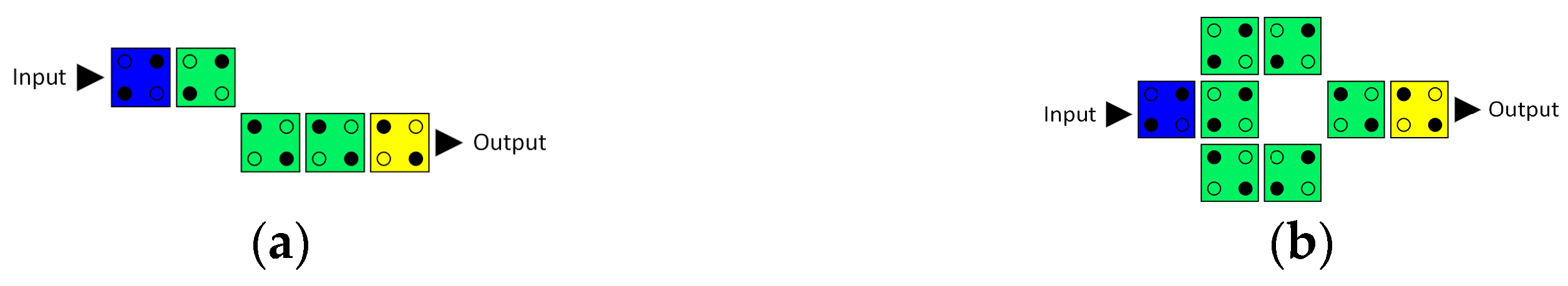
Figure 2.
(a) Logical synthesis of the conventional three-input majority gate. (b) Physical layout of the conventional QCA three-input majority gate. The blue colour indicates the input cells, the yellow colour indicates the output cell, and the green colour indicates the internal cells.
Figure 2.
(a) Logical synthesis of the conventional three-input majority gate. (b) Physical layout of the conventional QCA three-input majority gate. The blue colour indicates the input cells, the yellow colour indicates the output cell, and the green colour indicates the internal cells.

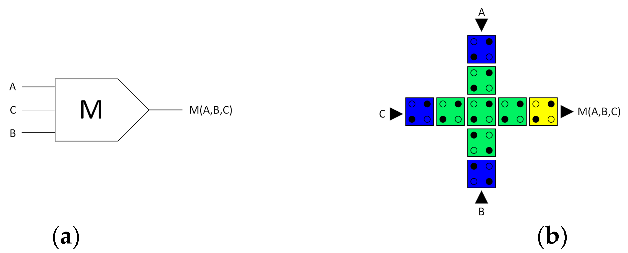
Figure 3.
(a) Logical synthesis of the three-input-three-output majority gate. (b) A USE clock zone containing the physical layout of the QCA three-input-three-output majority gate. The blue colour indicates the input cells, the yellow colour indicates the output cell, and the green colour indicates the internal cells.

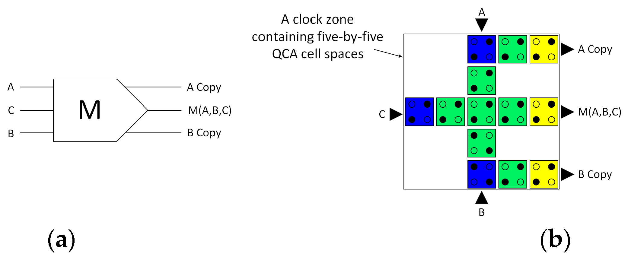
Figure 4.
(a) Logical synthesis of the reversible AND gate. (b) A USE clock zone containing the physical layout of the reversible QCA AND gate. The blue colour indicates the input cells, the yellow colour indicates the output cells, the green colour indicates the internal cells, and the orange cell with two electrons in the upper left and bottom right represents the cell with a fixed value of ‘0’.

Figure 5.
(a) Logical synthesis of the reversible OR gate. (b) A USE clock zone containing the physical layout of the reversible QCA OR gate. The blue colour indicates the input cells, the yellow colour indicates the output cells, the green colour indicates the internal cells, and the orange cell with two electrons in the upper right and bottom left represents the cell with a fixed value of ‘1’.

Figure 6.
(a) Synthesis of the proposed reversible 2:1 multiplexer. (b) Layout of the proposed reversible QCA 2:1 multiplexer (Acp, Bcp, Scp, and S′cp refer to copies of the input data, whereas g1 and g2 indicate garbage outputs).
Figure 6.
(a) Synthesis of the proposed reversible 2:1 multiplexer. (b) Layout of the proposed reversible QCA 2:1 multiplexer (Acp, Bcp, Scp, and S′cp refer to copies of the input data, whereas g1 and g2 indicate garbage outputs).

Figure 7.
(a) Schematic of the proposed reversible 4:1 multiplexer. (b) Layout of the proposed reversible QCA 4:1 multiplexer (Acp, Bcp, Ccp, Dcp, S0cp, S1cp, S0′cp, and S1′cp refer to copies of the input data, whereas g indicate garbage outputs).
Figure 7.
(a) Schematic of the proposed reversible 4:1 multiplexer. (b) Layout of the proposed reversible QCA 4:1 multiplexer (Acp, Bcp, Ccp, Dcp, S0cp, S1cp, S0′cp, and S1′cp refer to copies of the input data, whereas g indicate garbage outputs).

Figure 8.
(a) Schematic of the proposed reversible 8:1 multiplexer. (b) Layout of the proposed reversible 8:1 multiplexer (Acp, Bcp, Ccp, Dcp, Ecp, Fcp, Gcp, Hcp, S0cp, S1cp, S2cp, S0′cp, S1′cp, and S2′cp refer to copies of the input data, whereas g indicate garbage outputs).
Figure 8.
(a) Schematic of the proposed reversible 8:1 multiplexer. (b) Layout of the proposed reversible 8:1 multiplexer (Acp, Bcp, Ccp, Dcp, Ecp, Fcp, Gcp, Hcp, S0cp, S1cp, S2cp, S0′cp, S1′cp, and S2′cp refer to copies of the input data, whereas g indicate garbage outputs).


Table 1.
The adopted technological parameters.
| Parameter | Description | Value |
|---|---|---|
| QD size | Quantum-dot size | 5 nm |
| Cell area | Dimensions of each cell | 18 × 18 nm |
| Cell distance | Distance between two cells | 2 nm |
| Layer separation | Distance between QCA layers in multilayer crossing | 11.5 nm |
| Clock high | Max. saturation energy of clock signal | 9.8 × 10⁻²² J |
| Clock low | Min. saturation energy of clock signal | 3.8 × 10⁻²³ J |
| Relative permittivity | Relative permittivity of QCA materials (GaAs and AlGaAs) | 12.9 |
| Radius of effect | Maximum interaction distance between cells | 80 nm |
| Temp | Operating temperature | 1 K |
Table 2.
The employed simulation parameters.
| Parameter | Description | Value |
|---|---|---|
| τ | Relaxation time | 1 × 10⁻¹⁵ s |
| Tγ | Period of the clock signal | 1 × 10⁻⁹ s |
| Tin | Period of the input signals | 1 × 10⁻⁹ s |
| Tstep | Time interval of each iteration step | 1 × 10⁻¹⁶ s |
| Tsim | Total simulation time | 8 × 10⁻⁹ s |
| γshape | Shape of the clock signal slopes | Gaussian |
| γslope | Rise and fall time of the clock signal slopes | 1 × 10⁻¹⁰ s |
Table 3.
The truth table for the 2:1 multiplexer circuit depicted in Figure 6.
Table 3.
The truth table for the 2:1 multiplexer circuit depicted in Figure 6.
| S | Mux |
|---|---|
| 0 | A |
| 1 | B |
Table 4.
The truth table for the 4:1 multiplexer circuit depicted in Figure 7.
Table 4.
The truth table for the 4:1 multiplexer circuit depicted in Figure 7.
| S1 | S0 | Mux |
|---|---|---|
| 0 | 0 | A |
| 0 | 1 | B |
| 1 | 0 | C |
| 1 | 1 | D |
Table 5.
The truth table for the 8:1 multiplexer circuit depicted in Figure 8.
Table 5.
The truth table for the 8:1 multiplexer circuit depicted in Figure 8.
| S2 | S1 | S0 | Output |
|---|---|---|---|
| 0 | 0 | 0 | A |
| 0 | 0 | 1 | B |
| 0 | 1 | 0 | C |
| 0 | 1 | 1 | D |
| 1 | 0 | 0 | E |
| 1 | 0 | 1 | F |
| 1 | 1 | 0 | G |
| 1 | 1 | 1 | H |
Table 6.
Energy dissipation analysis of the proposed multiplexer. The average energy dissipation refers to the mean energy value averaged over the various input signal combinations.
Table 6.
Energy dissipation analysis of the proposed multiplexer. The average energy dissipation refers to the mean energy value averaged over the various input signal combinations.
| Proposed QCA Circuit | Total Energy Dissipation (meV) | Average Energy Dissipation (meV) |
|---|---|---|
| Reversible AND gate | 0.009 | 0.003 |
| Reversible OR gate | 0.009 | 0.002 |
| Reversible 2:1 multiplexer | 0.112 | 0.014 |
| Reversible 4:1 multiplexer | 0.525 | 0.057 |
| Reversible 8:1 multiplexer | 4.27 | 0.397 |
Table 7.
Multiplexers cost comparison.
| QCA Multiplexer Circuit | Used Inverters | Used AND Gates | Used OR Gates | QCA Cells | Area (µm) | Dealy (Clock Cycle) |
|---|---|---|---|---|---|---|
| Reversible 2:1 multiplexer | 1 | 2 | 1 | 56 | 0.09 | 1 |
| Reversible 4:1 multiplexer | 3 | 6 | 3 | 213 | 0.46 | 3 |
| Reversible 8:1 multiplexer | 7 | 14 | 7 | 646 | 1.36 | 5.5 |
Table 8.
Energy dissipation comparison of the 2:1 multiplexer circuit.
| QCA 2:1 Multiplexer | Total Energy Dissipation (meV) | Average Energy Dissipation (meV) |
|---|---|---|
| [35] | 16.20 | 1.38 |
| [36] | 15.20 | 1.38 |
| [37] | 13.86 | 1.29 |
| [38] | 12.40 | 1.14 |
| [39] | 11.30 | 1.02 |
| [34] | 8.91 | 0.810 |
| Proposed | 0.112 | 0.014 |
Disclaimer/Publisher’s Note: The statements, opinions and data contained in all publications are solely those of the individual author(s) and contributor(s) and not of MDPI and/or the editor(s). MDPI and/or the editor(s) disclaim responsibility for any injury to people or property resulting from any ideas, methods, instructions or products referred to in the content. |
© 2024 by the authors. Licensee MDPI, Basel, Switzerland. This article is an open access article distributed under the terms and conditions of the Creative Commons Attribution (CC BY) license (https://creativecommons.org/licenses/by/4.0/).
Share and Cite
MDPI and ACS Style
Alharbi, M.; Edwards, G.; Stocker, R. An Ultra-Energy-Efficient Reversible Quantum-Dot Cellular Automata 8:1 Multiplexer Circuit. Quantum Rep. 2024, 6, 41-57. https://0-doi-org.brum.beds.ac.uk/10.3390/quantum6010004
AMA Style
Alharbi M, Edwards G, Stocker R. An Ultra-Energy-Efficient Reversible Quantum-Dot Cellular Automata 8:1 Multiplexer Circuit. Quantum Reports. 2024; 6(1):41-57. https://0-doi-org.brum.beds.ac.uk/10.3390/quantum6010004
Chicago/Turabian StyleAlharbi, Mohammed, Gerard Edwards, and Richard Stocker. 2024. "An Ultra-Energy-Efficient Reversible Quantum-Dot Cellular Automata 8:1 Multiplexer Circuit" Quantum Reports 6, no. 1: 41-57. https://0-doi-org.brum.beds.ac.uk/10.3390/quantum6010004