1. Introduction
Digital single event transient (DSET) pulses are momentary glitch noises generated at logic gates by incident ions. They can dominate the heavy-ion-induced soft-error response of modern digital logic very-large-scale-integrations (VLSIs) [
1]. Since the pulse-width (duration) of DSETs is a key parameter in determining the soft error rates in logic VLSIs, the DSET pulse-widths have been extensively measured by using logic cell chains, and specially built pulse capture circuits such as variable temporal latches, self-triggering latches/flip-flops, and high drive-capability output-buffers [
2,
3,
4,
5,
6,
7,
8,
9,
10]. These circuits allow us to observe the widths of the DSET pulse originating in actual logic cells under ion irradiation test conditions. The heavy-ion-induced DSET pulse-widths and the DSET cross-sections in 0.2 µm fully-depleted silicon-on-insulator (FD-SOI) process inverter cells and NOR cells by using the on-chip self-triggering flip-flop latch chain named Snapshot has also been measured [
3,
7,
9,
10].
On the other hand, an analytical estimation method has been proposed to obtain the DSET pulse waveform generated in a logic cell from transient currents in a single MOSFET used in the logic cells [
11,
12,
13]. This method uses radiation-induced transient current waveforms from the off-state single MOSFET under various voltage conditions. The measured and/or simulated transient current waveforms are stored in a look-up table, and the DSET pulses are estimated within a table-based circuit simulation framework. For example, an FD-SOI process inverter cell is composed of an n-type MOSFET (nMOSFET) and a p-type MOSFET (pMOSFET). Thus, we can calculate the time variation of the logic out-put voltage from the time profile of the transient current with various supply bias conditions and static I-V characteristics of the other MOSFET in the inverter cell. By using this table-based estimation method, we can obtain realistic waveforms of the DSET pulses without the need of any external circuit such as variable temporal latches, self-triggering latches/flip-flops, and high drive-capability output-buffers. The estimation method has been verified by a comparison between the DSET pulse waveform estimated by using a simulated transient current waveform and the pulse-laser-induced DSET pulse waveform in an inverter cell measured by monitoring transistors [
14]. In other words, we can obtain realistic waveforms of the DSET pulses without the need of any irradiation experiments.
Since heavy-ions create actual initial charge (electron-hole pairs) distributions in MOSFETs, verification of the heavy-ion induced response based DEST pulse waveform estimation method has also been required. However, actual heavy-ion induced transient current waveforms from a single MOSFET have never been applied to the table-based estimation due to the uncertainty associated with the location of an ion strike within the MOSFET in the ion irradiation experiments. In principle, the transient current waveforms used in the table-based estimation method have to originate at the same location in the MOSFET under all voltage conditions.
In this paper, we used the table-based estimation method to estimate the heavy-ion-induced DSET pulse-widths in a single inverter (NOT) cell. We present a methodology for DSET pulse-width estimation from heavy-ion-induced current waveforms with various drain biases in a single n-type MOSFET. Then, we verify the pulse-width and our methodology by comparing our result to the previously measured DSET pulse-widths with a Snapshot circuit (self-triggering flip-flop latch chain).
2. Experimental
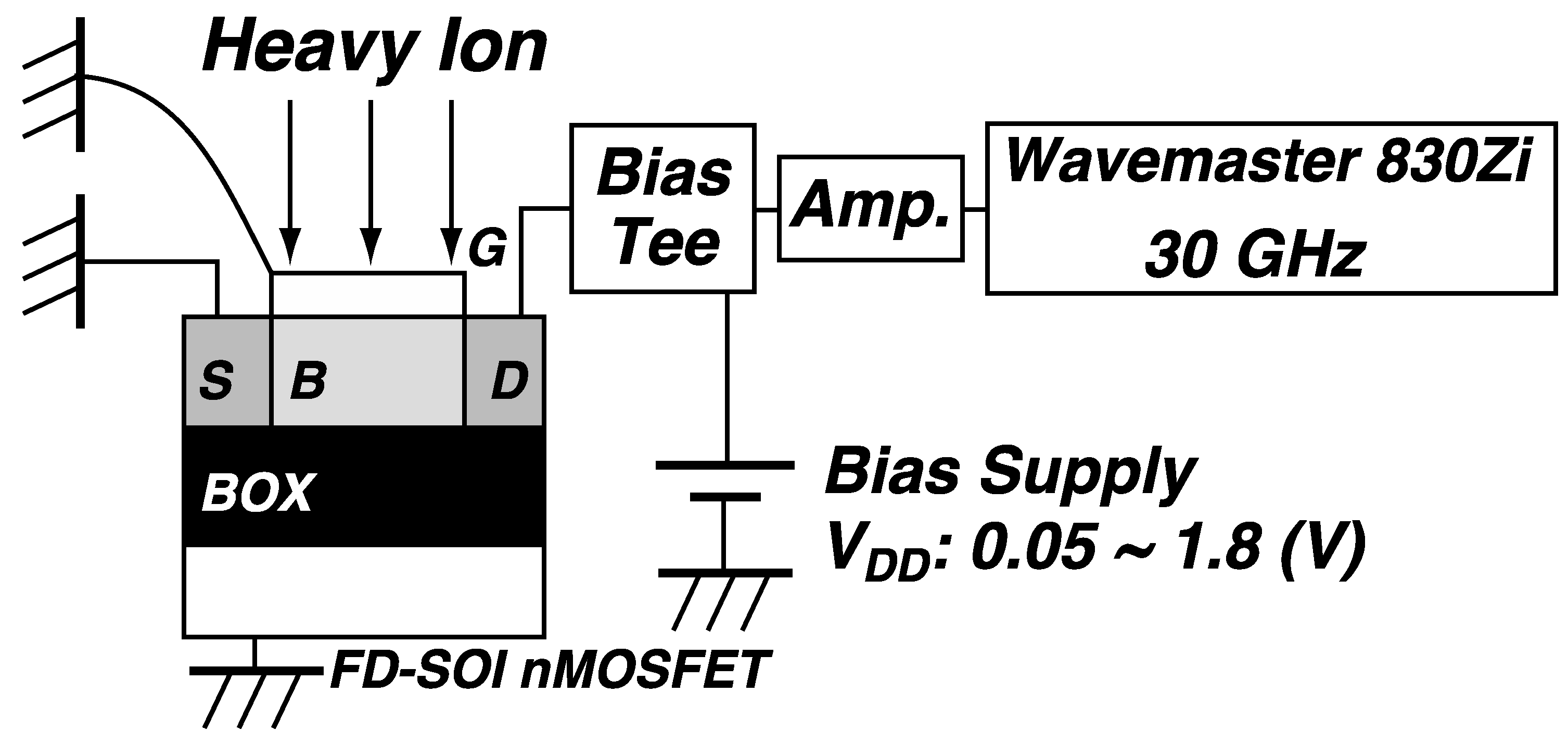
Figure 1 shows a schematic view of the experimental setup used in this study. The nMOSFET was fabricated by using a 0.2 µm FD-SOI process [
15]. The nMOSFET was mounted on a chip carrier with four strip-lines. Each electrode was connected to the corresponding strip-lines with short bonding wires. The gate width of the nMOSFET was 1.56 µm. The nMOSFET was configured as it is in an inverter and was used with self-triggering flip-flop latch chains [
3,
7,
9]. The nominal supply voltage of the process was 1.8 V. The transistor was biased in an off-state where its gate, source, and back-contact were grounded. Transient drain currents induced (I
Dn) by heavy-ion irradiation were measured with various drain biases. The drain’s voltage was varied from 1.8 V to 0.05 V with a power supply. Moreover, the drain bias was swept from 1.8 V to 0.2 V in 0.2 V steps, and from 0.2 V to 0.05 V in 0.05 V steps. Around 150–200 of transient current signals were collected at each drain bias condition. Unlike the tests with laser irradiation where a repetitive signal due to the same irradiation location can be generated and measured by a sampling oscilloscope, a single-shot oscilloscope was required for this study. Thus, we used a 30 GHz high-bandwidth single-shot digital oscilloscope (Model Wavemaster 830Zi) to measure the transient drain currents. It should be noted that the bias-tee, amplifier, and cables limited the bandwidth of the measurement system to 13.5 GHz in this study. The drain transient currents were amplified by a linear pre-amplifier with 21.5 dB before 50-Ω input to the oscilloscope.
The heavy-ion irradiation tests were performed using the azimuthally varying field (AVF) cyclotron at the Takasaki Ion Accelerators for Advanced Radiation Application (TIARA), National Institutes for Quantum and Radiological Science and Technology (QST), Takasaki. The test transistor was irradiated in a vacuum chamber with a broad beam of 322 MeV Krypton (Kr) from a direction perpendicular to the SOI layer to achieve an LET (liner energy transfer) of 40 MeV-cm
2/mg at the SOI surface. We assumed that the LET was constant in the SOI layer, since the projected ion range in the Si was 41 µm as evaluated by a SRIM (Stopping and Range of Ion in Matter) calculation [
16] and is enough to penetrate the very thin SOI layer without significant energy losses. The beam flux was measured by using a Si solid state detector, and controlled to the same flux as the DSET pulse-widths measurement in [
9].
3. Results and Discussion
3.1. Experimental Results
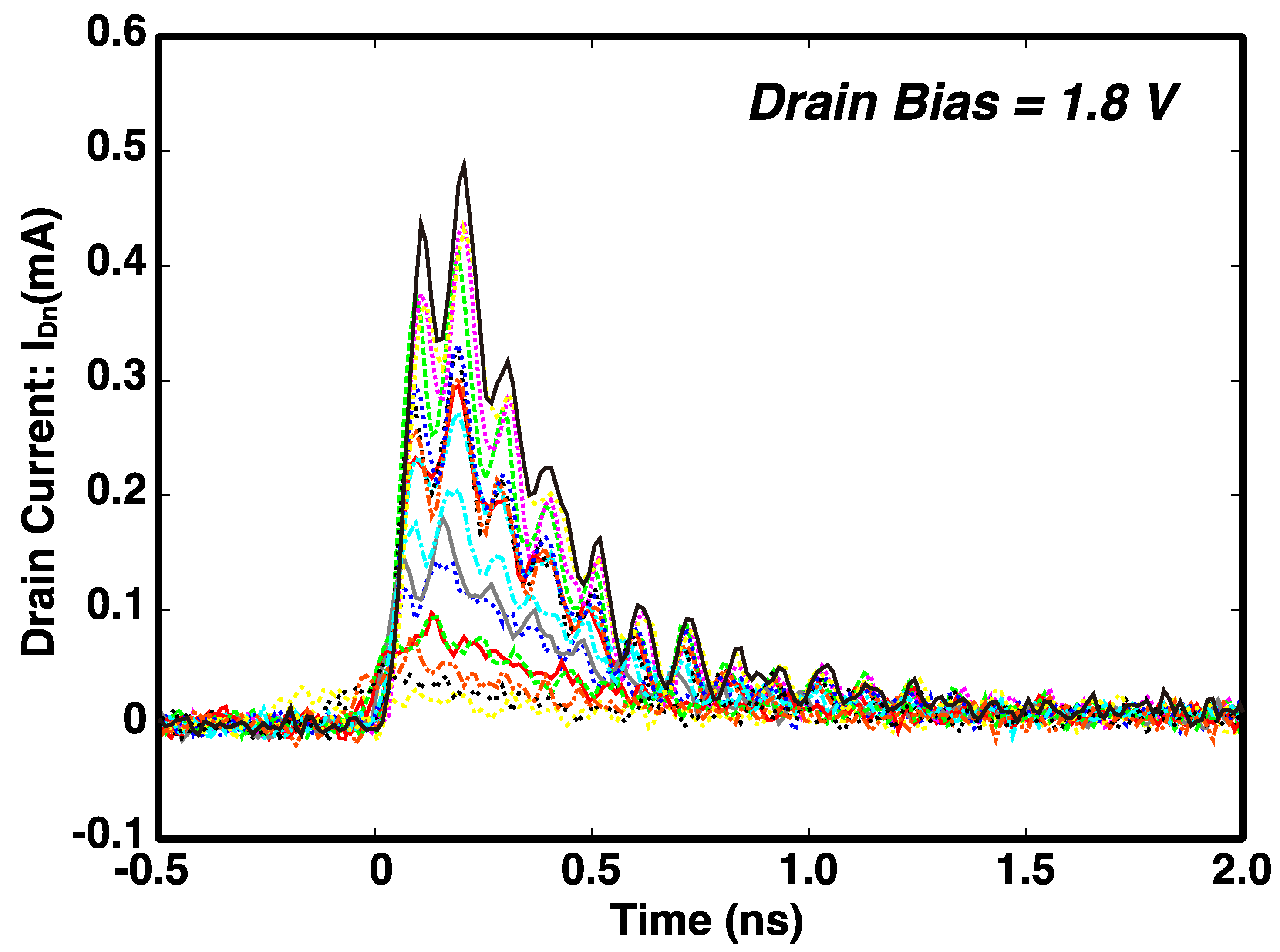
Figure 2 shows an example of the measured drain current waveforms at the drain bias of 1.8 V in the experiment. These sampled waveforms from all the measured drain current waveforms were plotted with colors to distinguish each waveform easily. The recorded waveforms exhibited fast rise times and exponentially decaying tails. The measured waveforms showed that the transient current response (pulse-height and decay time) varied even under constant-LET ion irradiation. This result can be explained by the fact that the current waveform varies depending on the location of the ion strikes in the transistor such as a gate hit or a drain hit as is the case for PD-SOI transistors [
17,
18]. The transient current was not recorded in the case of non-biased nMOSFET by ion incident, since no current pulses were measurable under this condition.
3.2. DSET Pulse-Width Estimation Methodology
As above-mentioned, the DSET pulse-width estimation method ideally requires the transient current waveforms to originate from the same strike location of ions in the MOSFET. However, in this study, it was not possible to obtain information on the relationship between the ion strike locations and the obtained current waveforms due to the use of a broad beam from the accelerator.
A correlation between the collected charge from a nominal biased MOSFET and the DSET pulse-widths in SOI devices was implied in [
17]. Thus, we extracted typical waveforms that had the greatest collected charge in each drain bias condition from the random transient current waveforms to estimate a typical DSET pulse waveform. Collected charges were calculated by a numerical integration of the recorded transient current waveforms.
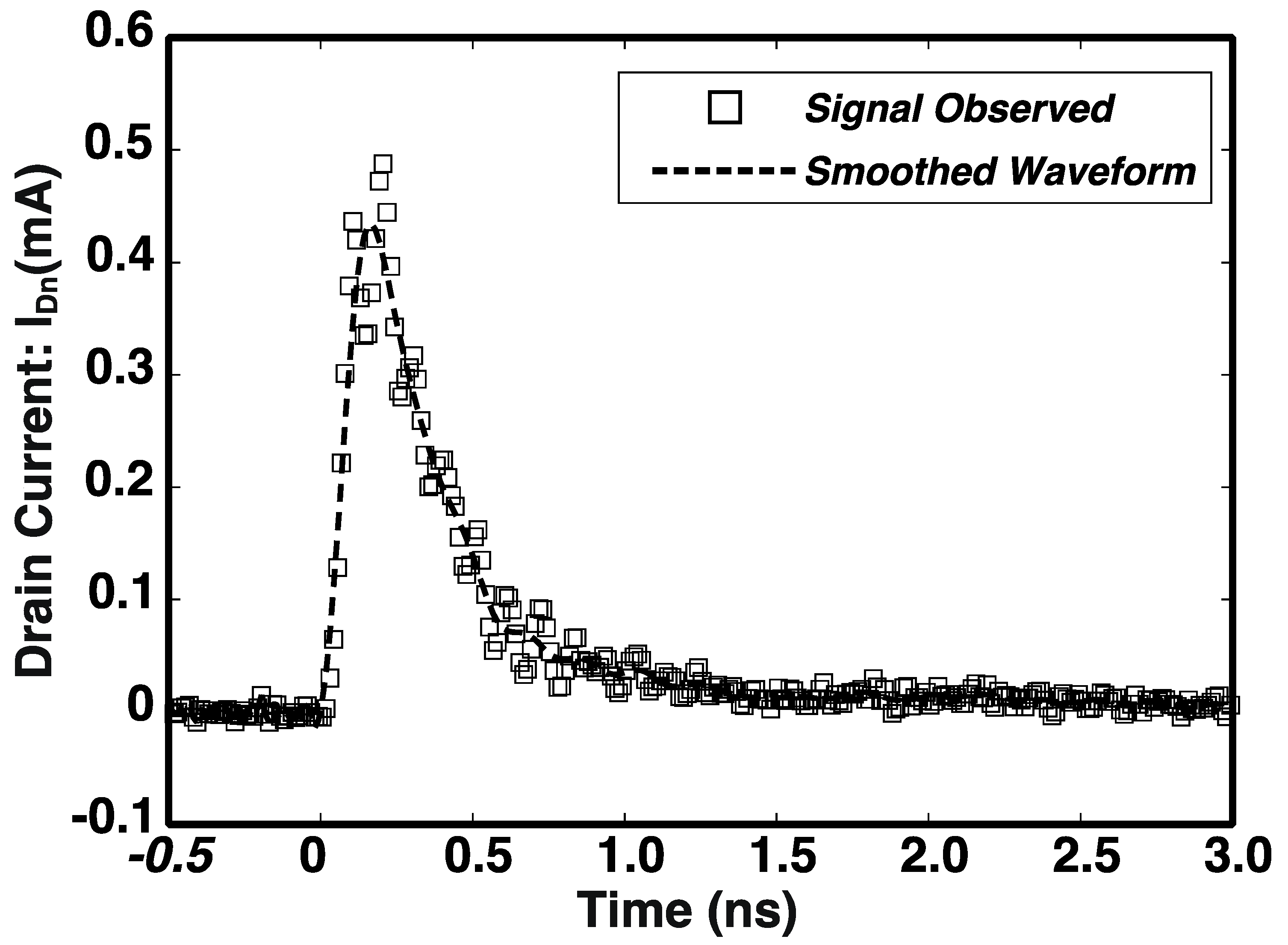
Figure 3 shows the extracted waveform from heavy-ion induced drain current waveforms, which had the greatest collected charge at the drain bias of 1.8 V. The waveform corresponds to the waveform plotted as the black solid line in
Figure 2. The measured waveform was also smoothed by the fast Fourier transform (FFT) method to minimize the effect of electronic noise. The smoothed waveform is also shown in
Figure 3 (broken line). For each drain bias condition, the smoothed transient current was derived in the same way.
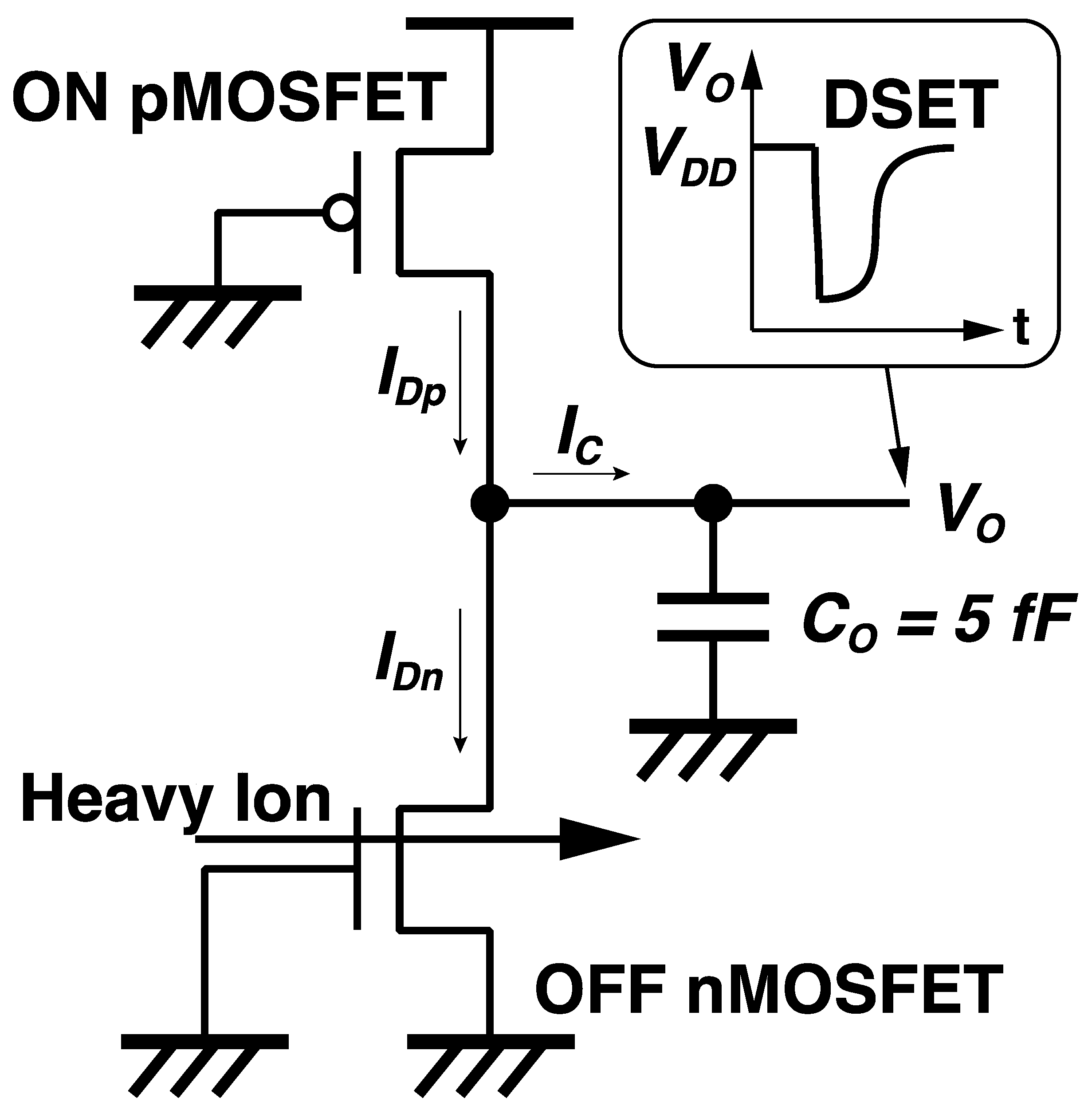
Figure 4 shows an equivalent circuit model of an inverter for the table-based estimation method (see [
11,
12,
13,
14] for further details of the table-based approach). The nMOSFET and the pMOSFET are modeled in the same configuration as it is used in an inverter connected to a self-triggering flip-flop latch chain to compare the estimated and the measured DSET pulse-widths.
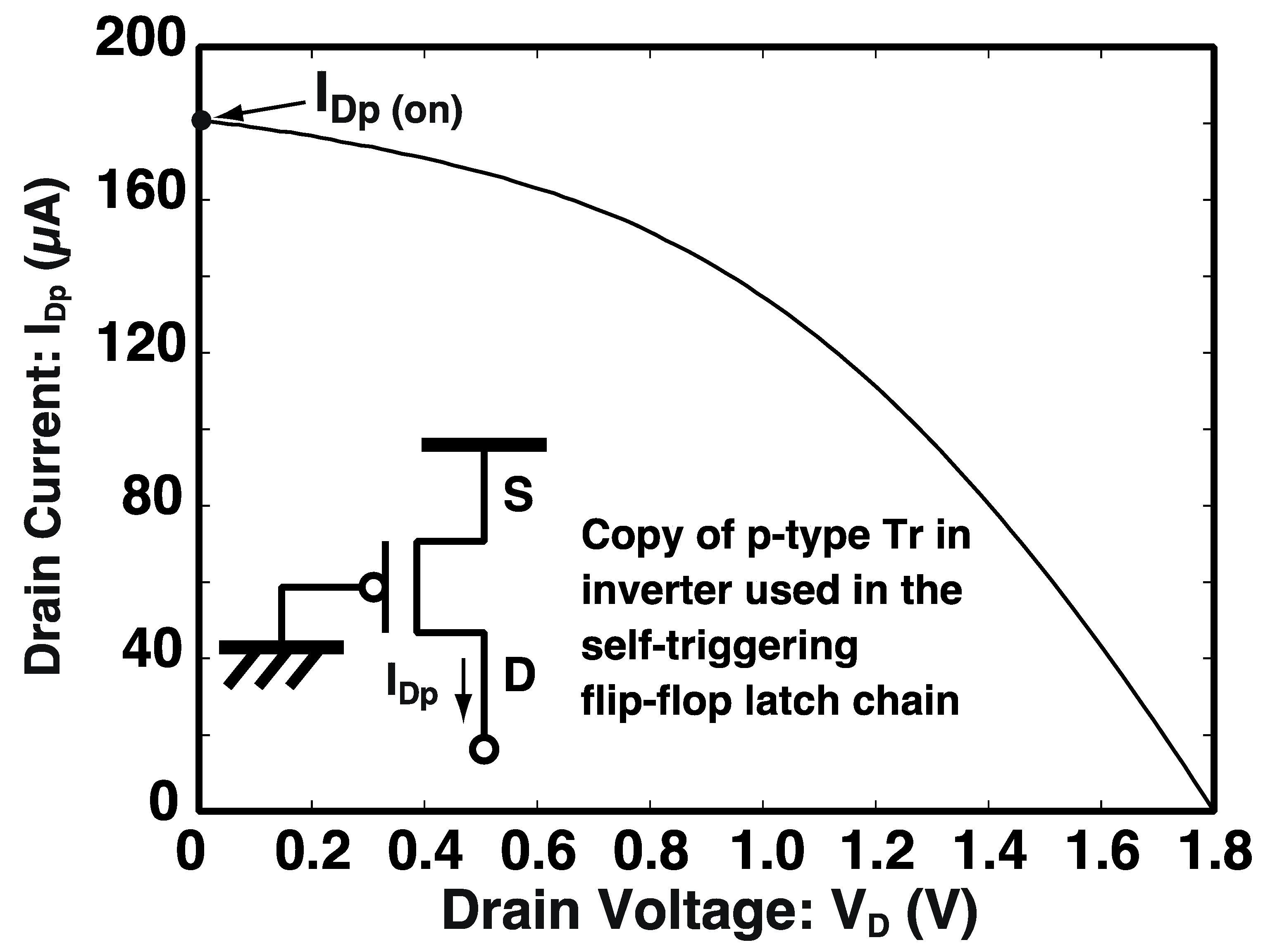
Figure 5 shows the measured statistic current-voltage characteristic of the actual pMOSFET. The gate width of the pMOSFET was 2.16 µm. We modeled the output capacitance C
O with a constant capacitance as a next stage inverter model. The value of C
O was theoretically estimated to be 5 fF from the design parameter of the inverter used in the self-triggering flip-flop latch chain. The DSET pulse waveform at V
O was determined from the table-based estimation method by using the measured current waveforms in the nMOSFET and the current-voltage characteristic of the pMOSFET.
3.3. DSET Pulse-Width Estimation Result
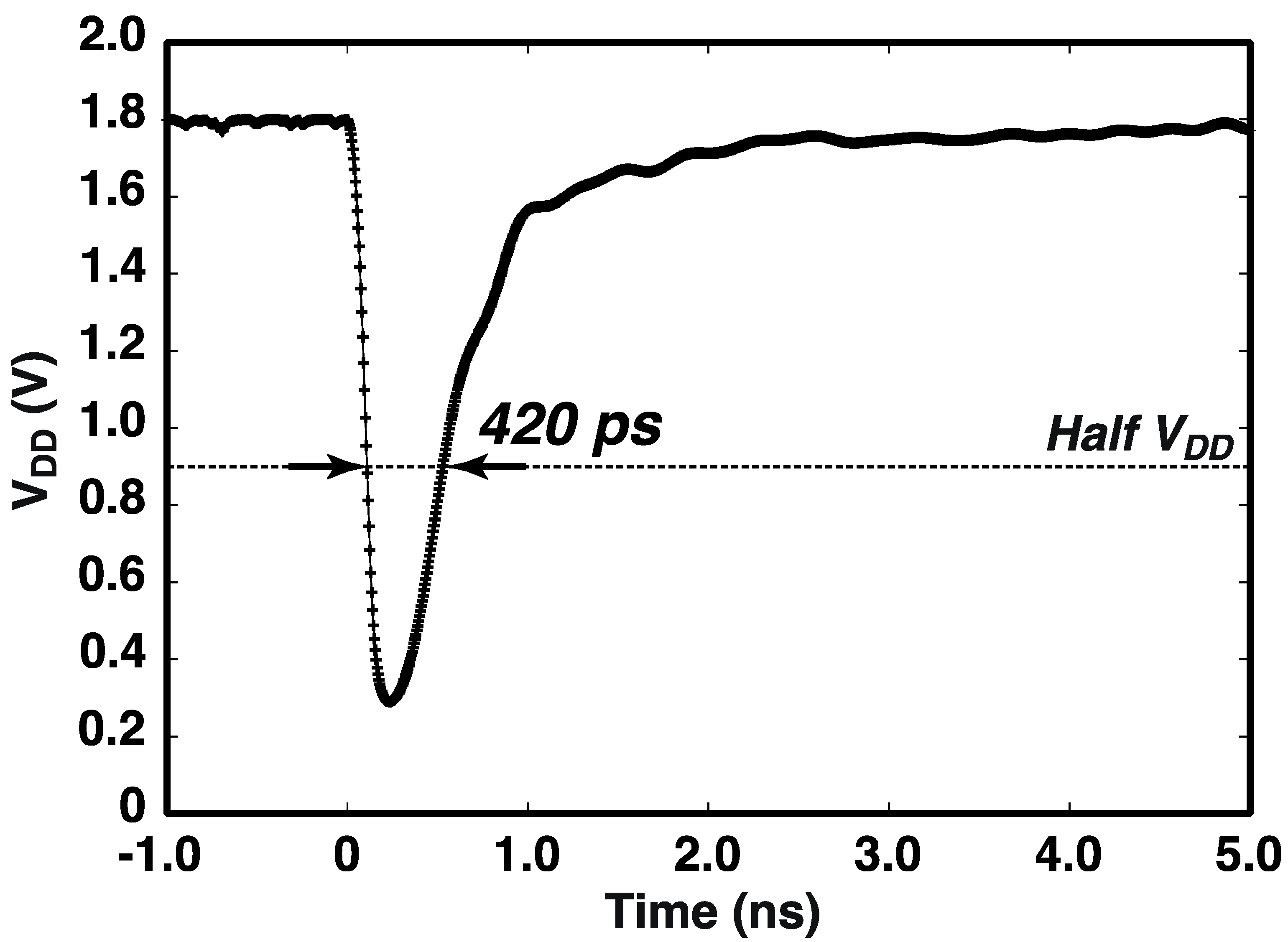
Figure 6 shows an estimated DSET waveform by using the table-based estimation method. This DSET pulse waveform shows the typical characteristics as the estimated waveforms in [
14] (e.g., fast falling edge and slow rising tail). This result indicates that our selection method of the current pulses can reconstruct the typical DSET waveforms. The DSET pulse-width is defined at half V
DD (drain voltage) of the transient voltage and was estimated to be 420 ps. The DSET pulse-width determined by the table-based estimation method was compared with the DSET pulse-widths measured by using the self-triggering flip-flop latch chain.
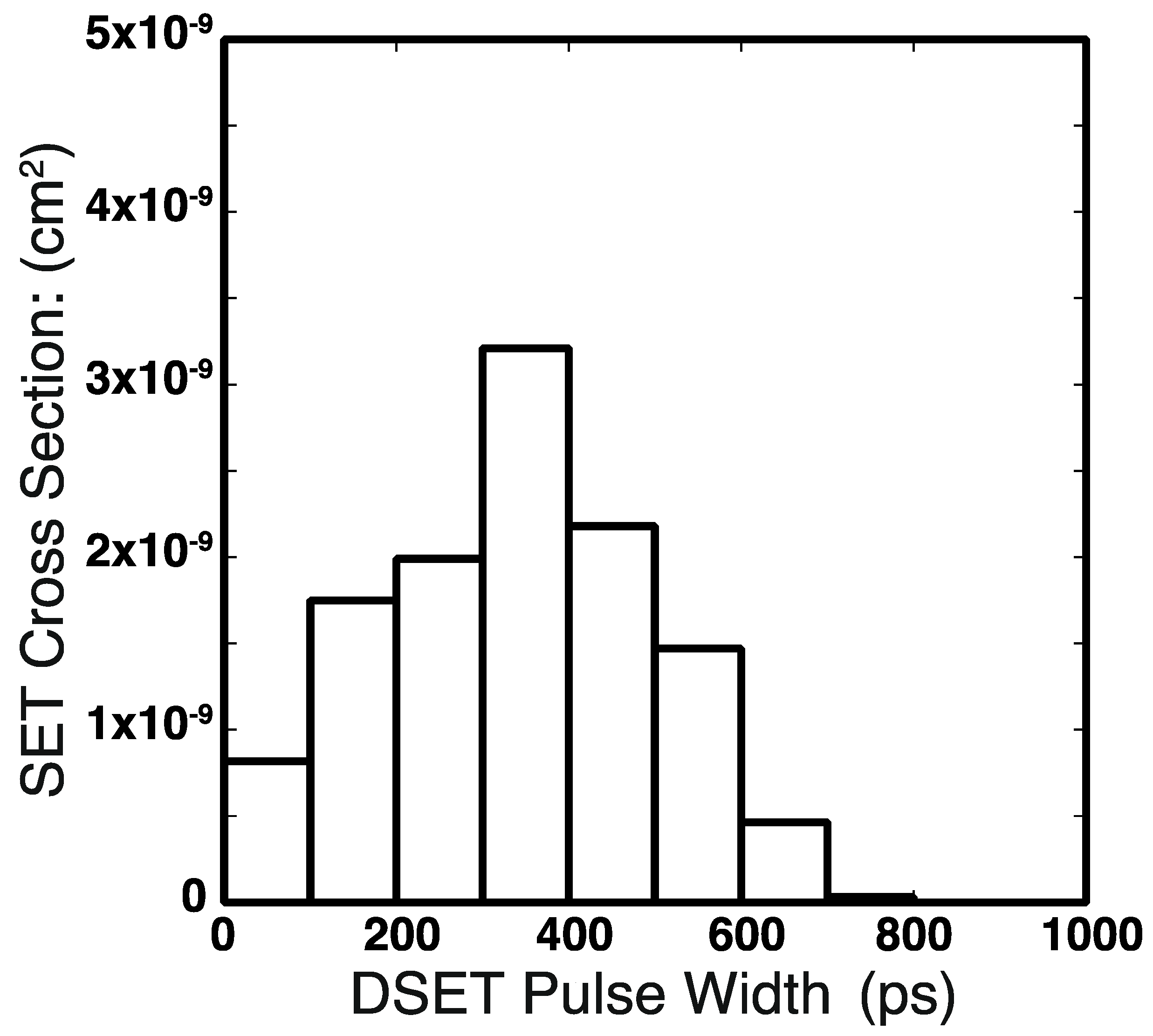
Figure 7 shows the DSET cross section (frequency) from a single inverter cell measured by using the self-triggering flip-flop latch chain in [
9]. The cross section was plotted as a function of the measured DSET pulse-width in the range up to 750 ps with a peak value at 350 ps. The DSET pulse-width of 420 ps estimated in this study fell within the range from the peak to the worst (longest) pulse-widths in the measured distribution by the self-triggering flip-flop latch chain. We were able to obtain information on the magnitude of the DSET pulse-width in a single inverter cell fabricated by FD-SOI technology by using this estimation method.
The estimated DSET pulse-width by this method was shorter than the measured worst DSET pulse-width (750 ps), though we used waveforms with the greatest collected charge at the drain bias of 1.8 V. In the present method, it is not possible to extract the transient current waveforms set from the MOSFET by having exactly the same position of ion strikes. Therefore, the worst DSET pulse-width must be underestimated. In addition, the bandwidth of the measurement system also contributed to the underestimation of the worst DSET pulse-width. Kobayashi et al. used pulse-laser and a measurement system with a bandwidth of 20 GHz to capture the irradiation response of single transistors, leading to a good agreement between the simulated DSET pulse-waveforms and the table-based estimated DSET pulse-waveform [
14]. On the other hand, the bandwidth of our measurement system was 13.5 GHz, and thus, the lower bandwidth of the measurement system resulted in an underestimation in the rise times and the amplitudes of the current pulses induced in the transistor.
4. Conclusions
We estimated the DSET waveform in an inverter from the measured drain currents originating from an nMOSFET fabricated with a 0.2 µm FD-SOI process by using a table-based estimation method. The DSET pulse-width was estimated to be 420 ps at half VDD. This was consistent with the measured DSET pulse-widths by using the self-triggering flip-flop latch chain, considering the measurement error. Applicability of the table-based DEST pulse waveform estimation method was verified in the case of heavy-ion-induced transient current based DSET pulse-width estimation.
Author Contributions
T.M., S.O., D.K. and K.H.; proposed the idea and the strategy for the experimental design. T.M., S.O. and D.K.; methodology and investigation, T.M., S.O., T.O., D.K., H.I. and K.H.; validation, T.M.; writing—original draft preparation, T.O., D.K., H.I. and K.H.; reviewing and editing the original draft of manuscript. All authors have read and agreed to the published version of the manuscript.
Conflicts of Interest
The authors declare no conflicts of interest.
References
- Buchner, S.; Baze, M.; Brown, D.; McMorrow, D.; Melinger, J. Comparison of error rates in combinational and sequential logic. IEEE Trans. Nucl. Sci. 1997, 44, 2209–2216. [Google Scholar] [CrossRef]
- Benedetto, J.M.; Eaton, P.H.; Mavis, D.G.; Gadlage, M.; Turflinger, T. Variation of digital SET pulse-widths and the implication for single event hardening of advanced CMOS processes. IEEE Trans. Nucl. Sci. 2005, 52, 2114–2119. [Google Scholar] [CrossRef]
- Yanagawa, Y.; Hirose, K.; Saito, H.; Kobayashi, D.; Fukuda, S.; Ishii, S.; Takahashi, D.; Kuroda, Y. Direct measurement of SET pulse width in 0.2-µm SOI logic cells irradiated by heavy ion. IEEE Trans. Nucl. Sci. 2006, 53, 3575–3578. [Google Scholar] [CrossRef]
- Narasimham, B.; Bhuva, B.L.; Schrimpf, R.D.; Massengill, L.W.; Gadlage, M.J.; Amusan, O.A.; Holman, W.T.; Witulski, A.F.; Robinson, W.H.; Benedetto, J.M.; et al. Characterization of digital single event transient pulse-widths in 130-nm and 90-nm CMOS Technologies. IEEE Trans. Nucl. Sci. 2007, 54, 2506–2511. [Google Scholar] [CrossRef]
- Ferlet-Cavrois, V.; Paillet, P.; McMorrow, D.; Fel, N.; Baggio, J.; Girard, S.; Duhamel, O.; Melinger, J.S.; Gaillardin, M.; Schwank, J.R.; et al. New insight into single event transient propagation in chains of inverters -Evidence for propagation-induced pulse broadening. IEEE Trans. Nucl. Sci. 2007, 54, 2338–2346. [Google Scholar] [CrossRef]
- Ferlet-Cavrois, V.; Pouget, V.; McMorrow, D.; Schwank, J.R.; Fel, N.; Essely, F.; Flores, R.S.; Paillet, P.; Gaillardin, M.; Kobayashi, D.; et al. Investigation of the propagation induced pulse broadening (PIPB) effect in SOI and bulk inverter chains. IEEE Trans. Nucl. Sci. 2008, 55, 2842–2853. [Google Scholar] [CrossRef]
- Makino, T.; Kobayashi, D.; Hirose, K.; Yanagawa, Y.; Saito, H.; Ikeda, H.; Takahashi, D.; Ishii, S.; Kusano, M.; Onoda, S.; et al. LET dependence of single event transient pulse-width in SOI logic cell. IEEE Trans. Nucl. Sci. 2009, 56, 202–207. [Google Scholar] [CrossRef]
- Gadlage, M.J.; Gouker, P.; Bharat, B.L.; Narasimham, B.; Schrimpf, R.D. Heavy-ion-induced digital single event transients in a 180 nm fully depleted SOI process. IEEE Trans. Nucl. Sci. 2009, 56, 3483–3488. [Google Scholar] [CrossRef]
- Makino, T.; Kobayashi, D.; Hirose, K.; Takahashi, D.; Ishii, S.; Kusano, M.; Onoda, S.; Hirao, T.; Ohshima, T. Soft-error rate in a logic LSI estimated from SET pulse-width measurements. IEEE Trans. Nucl. Sci. 2009, 56, 3180–3184. [Google Scholar] [CrossRef]
- Yanagawa, Y.; Kobayashi, D.; Hirose, K.; Makino, T.; Saito, H.; Ikeda, H.; Onoda, S.; Hirao, T.; Ohshima, T. Experimental verification of scan-architecture-based evaluation technique of SET and SEU soft-error rates at each flip-flop in logic LSI systems. IEEE Trans. Nucl. Sci. 2009, 56, 1958–1963. [Google Scholar] [CrossRef]
- Kobayashi, D.; Hirose, K.; Ikeda, H.; Saito, H. Fast and physically-accurate estimation of single event transient pulses from radiation-induced transient currents measured in a single MOSFET: A simulation-based case study in bulk CMOS logic circuit. In Proceedings of the 2007 IEEE Workshop on Silicon Errors in Logic--System Effects (SELSE3), Austin, TX, USA, 3–4 April 2007. [Google Scholar]
- Kobayashi, D.; Saito, H.; Hirose, K. Estimation of single event transient voltage pulses in LSI circuits from heavy-ion-induced transient currents measured in a single MOSFET. IEEE Trans. Nucl. Sci. 2007, 54, 1037–1041. [Google Scholar] [CrossRef]
- Kobayashi, D.; Hirose, K.; Makino, T.; Ikeda, H.; Saito, H. Feasibility study of a table-based SET-pulse estimation in logic cell from heavy-ion-induced transient current measured in a single MOSFET. IEEE Trans. Nucl. Sci. 2007, 54, 2347–2354. [Google Scholar] [CrossRef]
- Kobayashi, D.; Hirose, K.; Ferlet-Cavrois, V.; McMorrow, D.; Makino, T.; Ikeda, H.; Arai, Y.; Ohno, M. Waveform observation of digital single-event transients employing monitoring transistor technique. IEEE Trans. Nucl. Sci. 2008, 55, 2872–2879. [Google Scholar] [CrossRef]
- Hirose, K.; Saito, H.; Kuroda, Y.; Ishii, S.; Fukuoka, Y.; Takahashi, D. SEU resistance in advanced SOI-SRAMs fabricated by commercial technology using a rad-hard circuit design. IEEE Trans. Nucl. Sci. 2002, 49, 2965–2968. [Google Scholar] [CrossRef]
- Zigler, J.F. Program SRIM/TRIM. Available online: http://www.srim.org (accessed on 2 March 2020).
- Ferlet-Cavrois, V.; Paillet, P.; Gaillardin, M.; Lambert, D.; Baggio, J.; Schwank, J.R.; Vizkelethy, G.; Shaneyfelt, M.R.; Hirose, K.; Blackmore, E.W.; et al. Statistical analysis of the charge collected in SOI and bulk devices under heavy ion irradiation -- implications for digital SETs. IEEE Trans. Nucl. Sci. 2006, 53, 3242–3252. [Google Scholar] [CrossRef]
- Castellani-Coulie, K.; Munteanu, D.; Ferlet-Cavrois, V.; Autran, J.L. Simulation analysis of the bipolar amplification in fully-depleted SOI technologies under heavy-ion irradiation. IEEE Trans. Nucl. Sci. 2005, 52, 1474–1479. [Google Scholar] [CrossRef]
© 2020 by the authors. Licensee MDPI, Basel, Switzerland. This article is an open access article distributed under the terms and conditions of the Creative Commons Attribution (CC BY) license (http://creativecommons.org/licenses/by/4.0/).

 ,
, 


