Time Multiplexed Active Neural Probe with 1356 Parallel Recording Sites

 , , , and
Abstract
:1. Introduction
2. Operation Principles
2.1. Overview
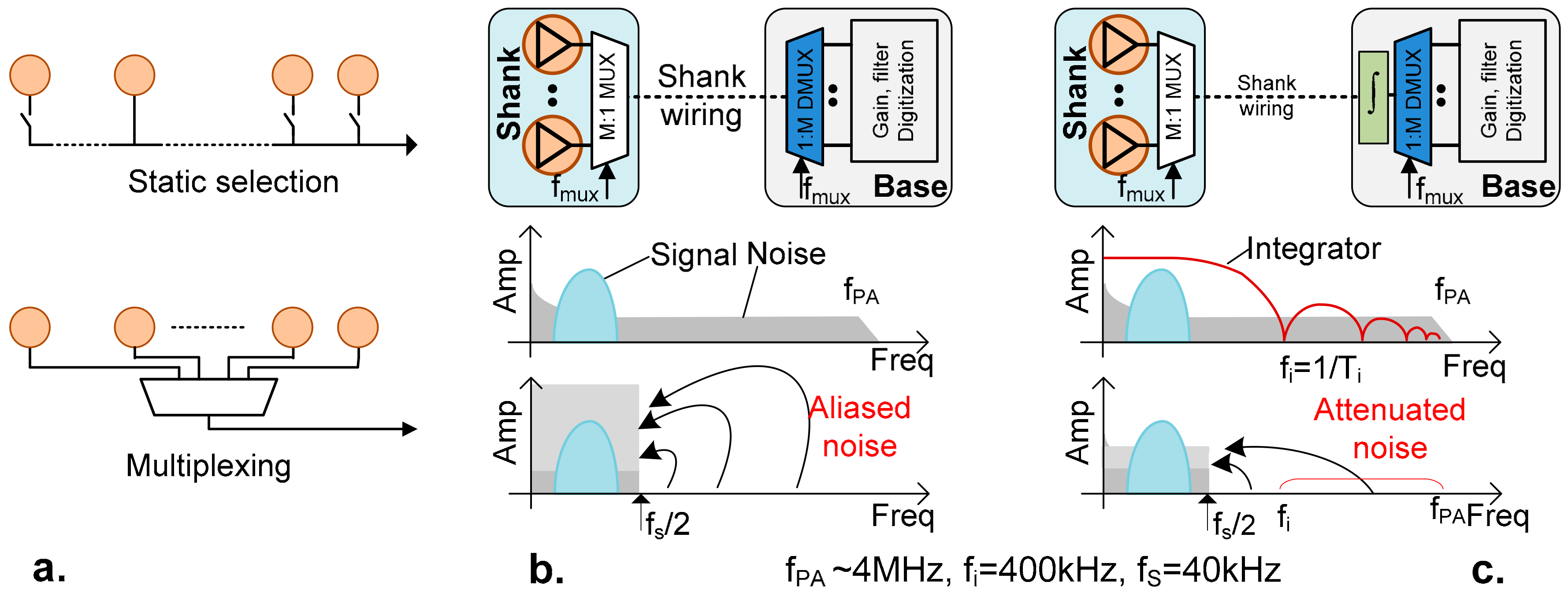
2.2. Noise Folding
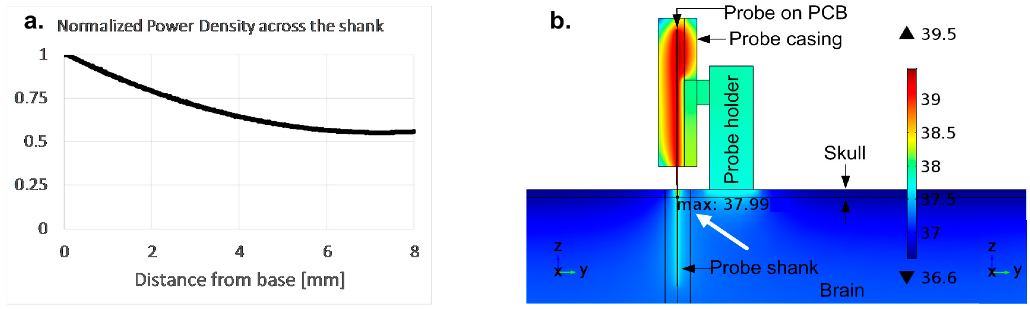
2.3. Power Limitation
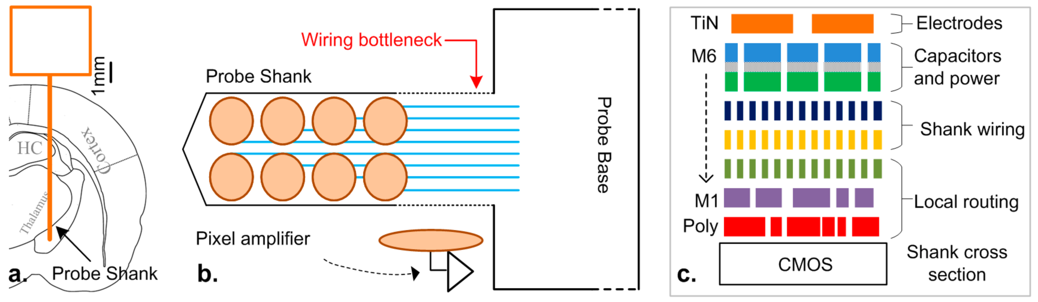
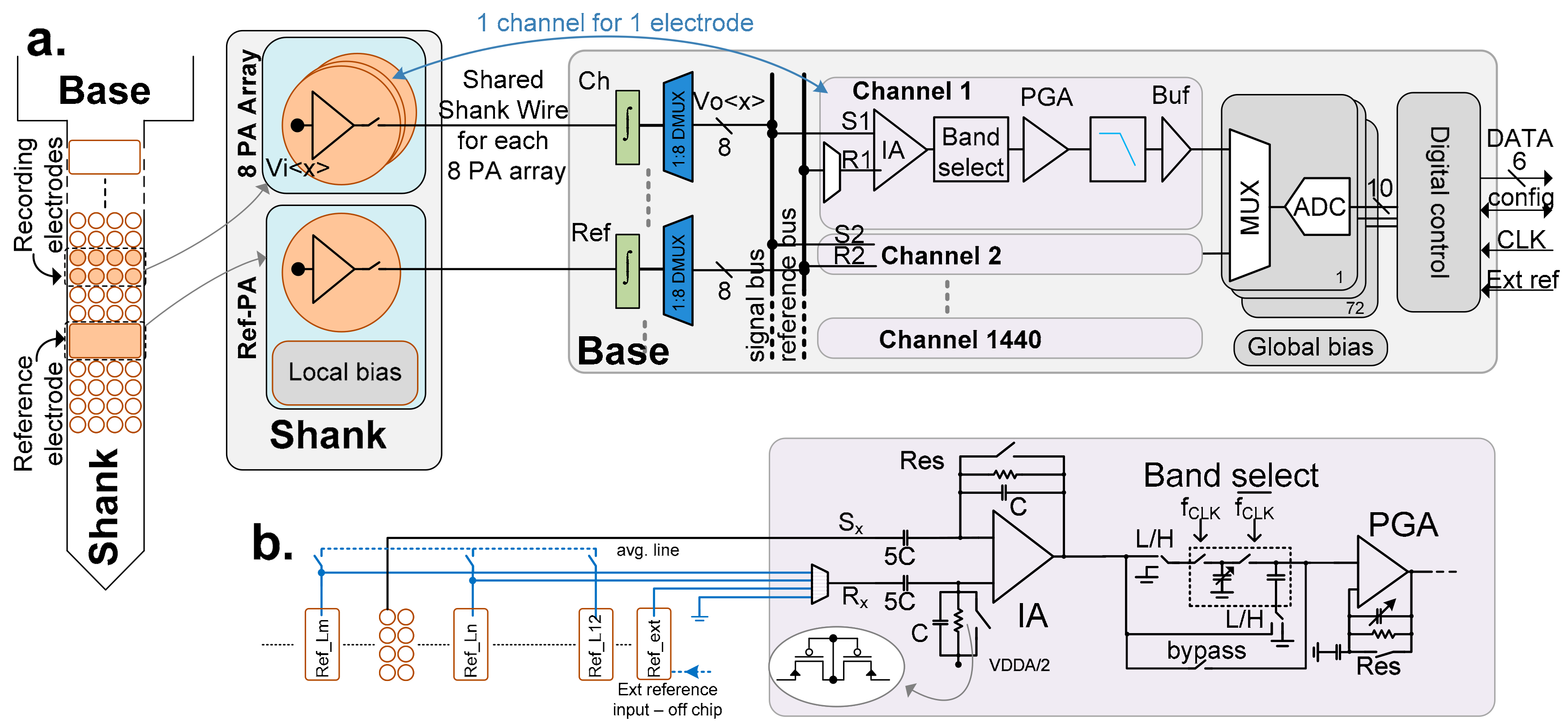
3. Architecture
4. Circuit Description
4.1. Pixel
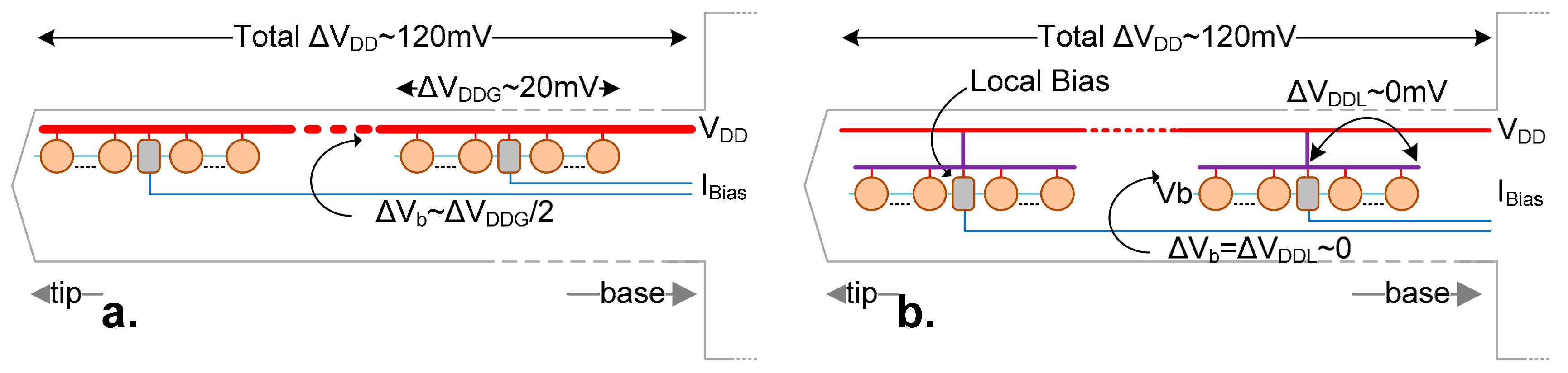
4.2. Shank Power Supply
4.3. Calibration and Reset
4.4. Recording Performance
4.5. Channel
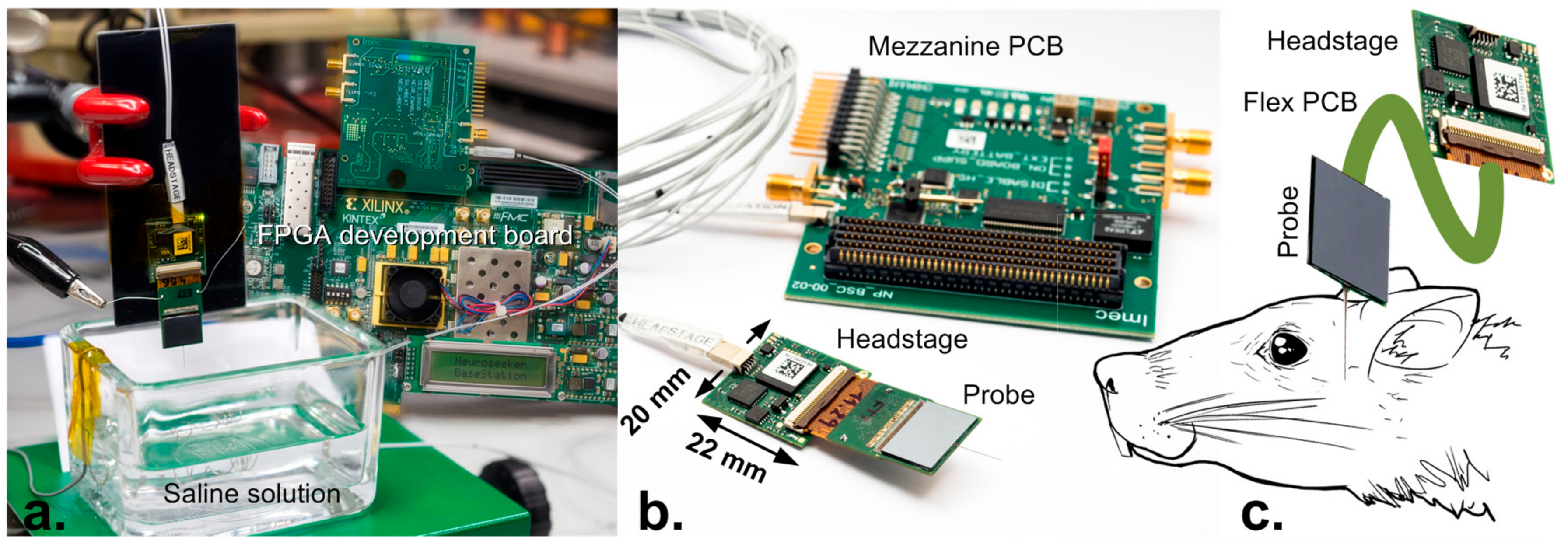
5. Device Fabrication
6. System
7. Test Results
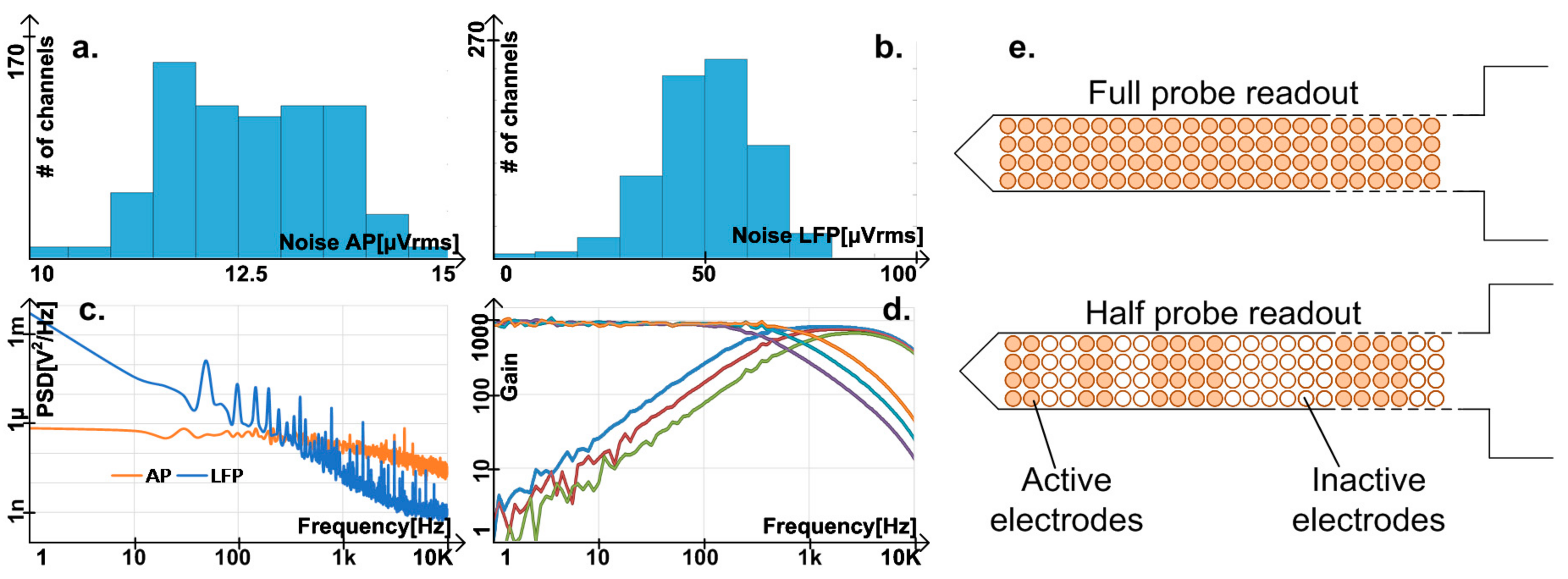
7.1. Electrical Performance
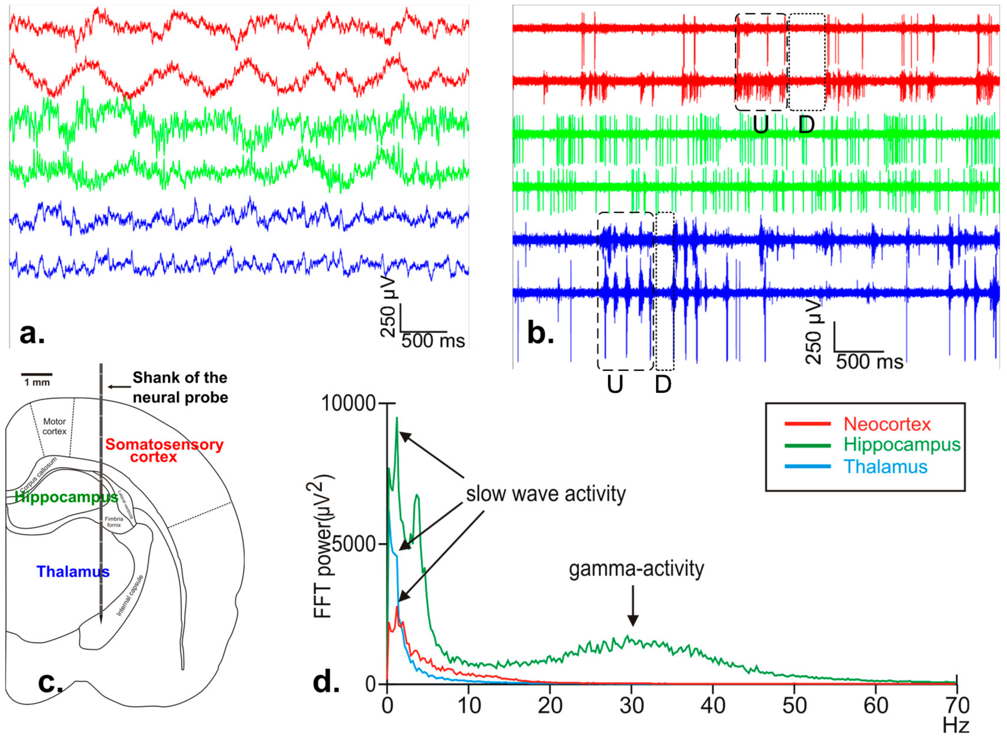
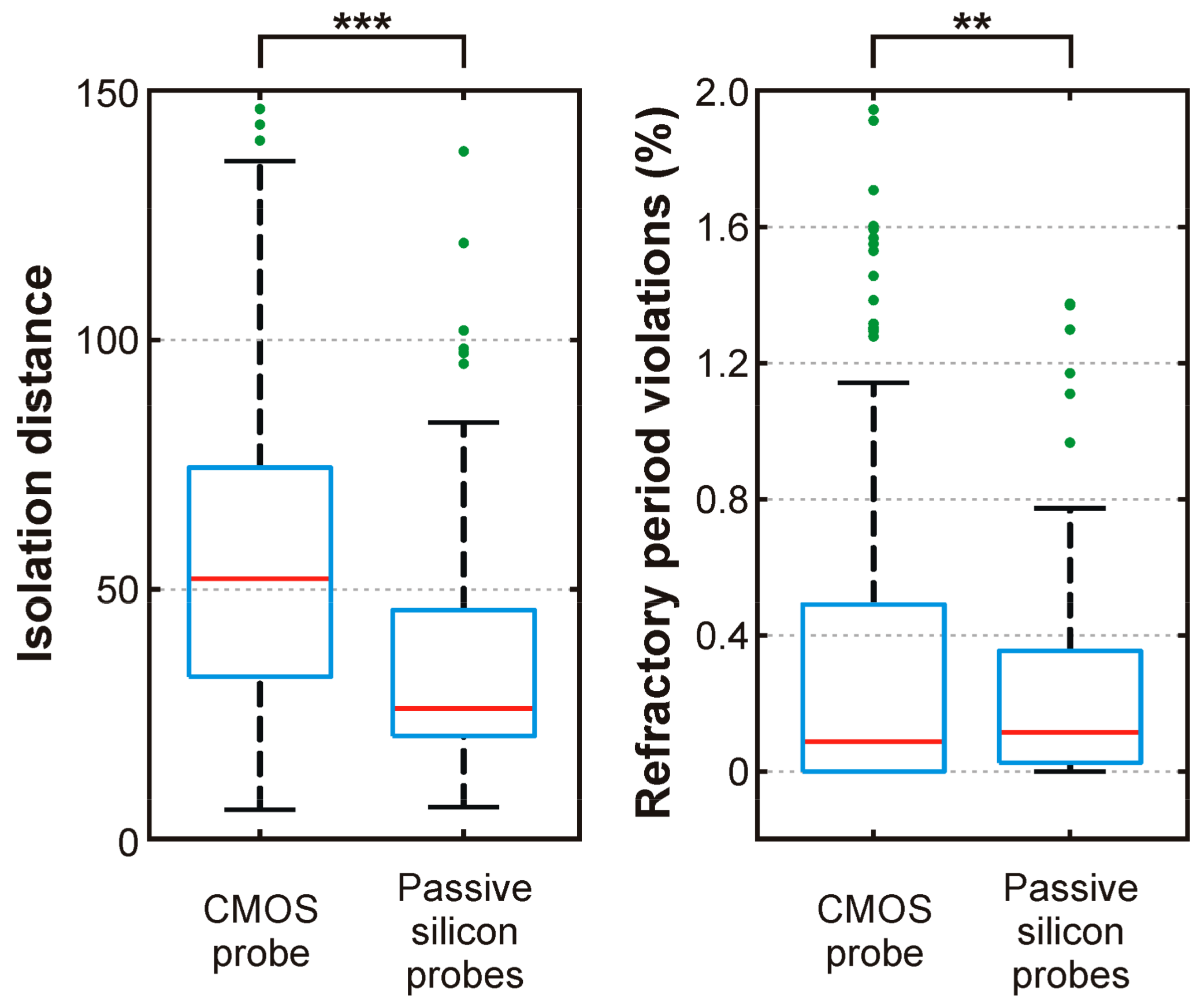
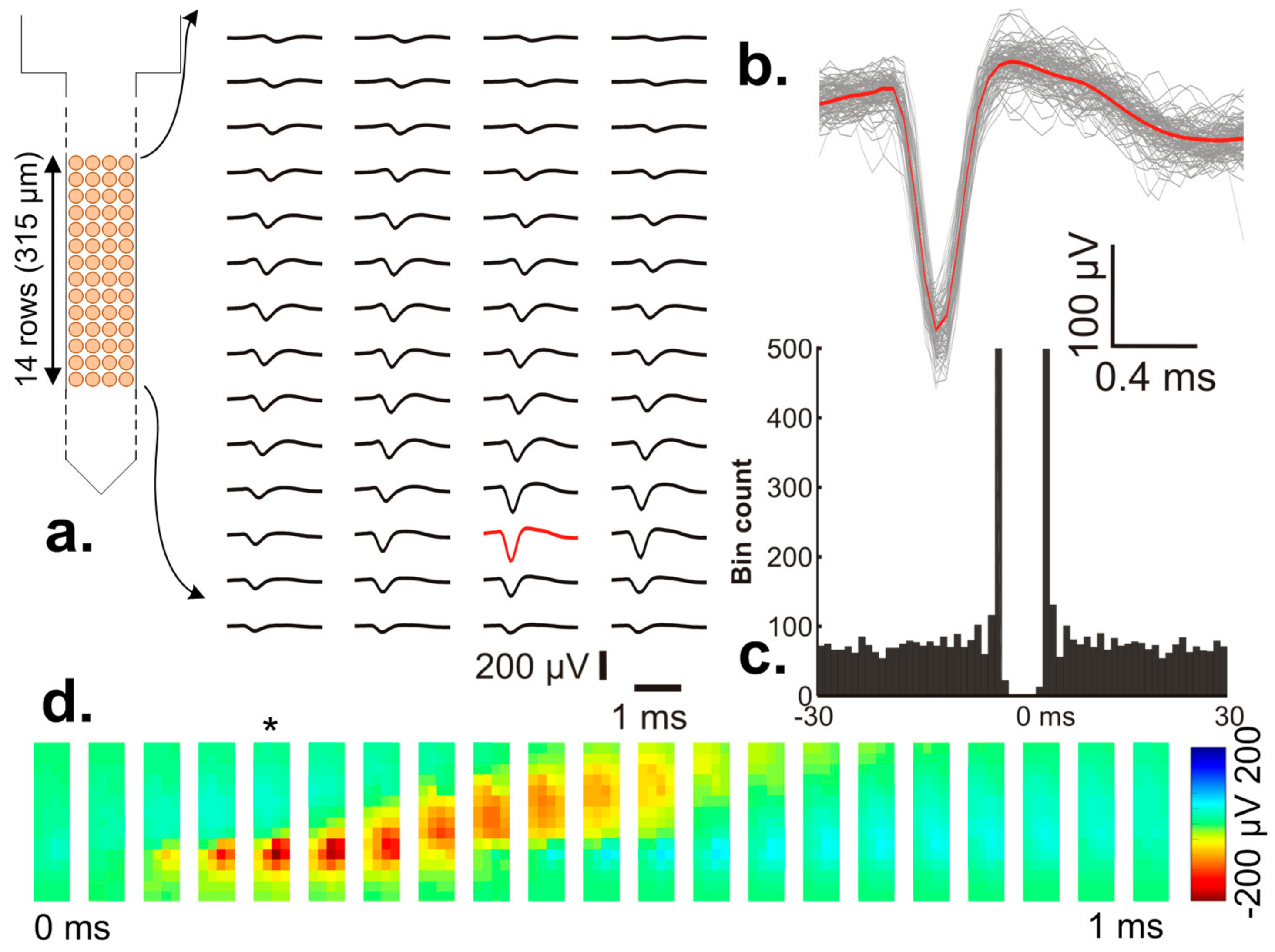
7.2. In-Vivo Neural Recordings
8. Conclusions
Acknowledgments
Author Contributions
Conflicts of Interest
References
- Buzsáki, G.; Stark, E.; Berényi, A.; Khodagholy, D.; Kipke, D.R.; Yoon, E.; Wise, K.D. Tools for probing local circuits: High-density silicon probes combined with optogenetics. Neuron 2015, 86, 92–105. [Google Scholar] [CrossRef] [PubMed]
- Lopez, C.M.; Andrei, A.; Mitra, S.; Welkenhuysen, M.; Eberle, W.; Bartic, C.; Puers, R.; Yazicioglu, R.F.; Gielen, G.G.E. An Implantable 455-Active-Electrode 52-Channel CMOS Neural Probe. IEEE J. Solid-State Circuits 2014, 49, 248–261. [Google Scholar] [CrossRef]
- Olsson, R.H.; Wise, K.D. A three-dimensional neural recording microsystem with implantable data compression circuitry. IEEE J. Solid-State Circuits 2005, 40, 2796–2804. [Google Scholar] [CrossRef]
- Lopez, C.M.; Putzeys, J.; Raducanu, B.C.; Ballini, M.; Wang, S.; Andrei, A.; Rochus, V.; Vandebriel, R.; Severi, S.; Van Hoof, C.; et al. A neural probe with up to 966 electrodes and up to 384 configurable channels in 0.13 µm SOI CMOS. IEEE Trans. Biomed. Circuits Syst. 2017, 11, 510–522. [Google Scholar] [CrossRef] [PubMed]
- Raducanu, B.C.; Yazicioglu, R.F.; Lopez, C.M.; Ballini, M.; Putzeys, J.; Wang, S.; Andrei, A.; Welkenhuysen, M.; van Helleputte, N.; Musa, S.; et al. Time multiplexed active neural probe with 678 parallel recording sites. In Proceedings of the 2016 46th European Solid-State Device Research Conference (ESSDERC), Lausanne, Switzerland, 12–15 September 2016; pp. 385–388. [Google Scholar]
- Harrison, R.R. A Versatile Integrated Circuit for the Acquisition of Biopotentials. In Proceedings of the IEEE 2007 Custom Integrated Circuits Conference (CICC 2007), San Jose, CA, USA, 16–19 September 2007; pp. 115–122. [Google Scholar]
- Huang, Y.C.; Huang, P.T.; Wu, S.L.; Hu, Y.C.; You, Y.H.; Chen, M.; Huang, Y.Y.; Chang, H.C.; Lin, Y.H.; Duann, J.R.; et al. An ultra-high-density 256-channel/25mm2 neural sensing microsystem using TSV-embedded neural probes. In Proceedings of the 2016 IEEE International Symposium on Circuits and Systems (ISCAS), Montreal, QC, Canada, 22–25 May 2016; pp. 1302–1305. [Google Scholar]
- Szuts, T.A.; Fadeyev, V.; Kachiguine, S.; Sher, A.; Grivich, M.V.; Agrochão, M.; Hottowy, P.; Dabrowski, W.; Lubenov, E.V.; Siapas, A.G.; et al. A wireless multi-channel neural amplifier for freely moving animals. Nat. Neurosci. 2011, 14, 263–269. [Google Scholar] [CrossRef] [PubMed]
- Herbawi, A.S.; Larramendy, F.; Galchev, T.; Holzhammer, T.; Mildenberger, B.; Paul, O.; Ruther, P. CMOS-based neural probe with enhanced electronic depth control. In Proceedings of the 2015 Transducers—2015 18th International Conference on Solid-State Sensors, Actuators and Microsystems (TRANSDUCERS), Anchorage, AK, USA, 21–25 June 2015; pp. 1723–1726. [Google Scholar]
- Shandhi, M.M.H.; Leber, M.; Hogan, A.; Bhandari, R.; Negi, S. A novel method of fabricating high channel density neural array for large neuronal mapping. In Proceedings of the he 2015 Transducers—2015 18th International Conference on Solid-State Sensors, Actuators and Microsystems (TRANSDUCERS), Anchorage, AK, USA, 21–25 June 2015; pp. 1759–1762. [Google Scholar]
- Santhanam, G.; Linderman, M.D.; Gilja, V.; Afshar, A.; Ryu, S.I.; Meng, T.; Shenoy, K. Hermes: A Continuous Neural Recording System for Freely Behaving Primates. IEEE Trans. Biomed. Eng. 2007, 54, 2037–2050. [Google Scholar] [CrossRef] [PubMed]
- Yazicioglu, F.; Lopez, C.M.; Mitra, S.; Raducanu, B.; Musa, S. Ultra-High-Density In-Vivo Neural Probes. In Proceedings of the 36th Annual International Conference of the IEEE Engineering in Medicince and Biology Society, Chicago, IL, USA, 26–30 August 2014; pp. 2032–2035. [Google Scholar]
- Du, J.; Blanche, T.J.; Harrison, R.R.; Lester, H.A.; Masmanidis, S.C. Multiplexed, high density electrophysiology with nanofabricated neural probes. PLoS ONE 2011, 6, e26204. [Google Scholar] [CrossRef] [PubMed]
- Scholvin, J.; Kinney, J.P.; Bernstein, J.G.; Moore-Kochlacs, C.; Kopell, N.; Fonstad, C.G.; Boyden, E.S. Close-packed silicon microelectrodes for scalable spatially oversampled neural recording. IEEE Trans. Biomed. Eng. 2016, 63, 120–130. [Google Scholar] [CrossRef] [PubMed]
- Sayed Herbawi, A.; Kießner, L.; Paul, O.R.P. High-density CMOS neural probe implementing a hierarchical addressing scheme for 1600 recording sites and 32 output channels. In Proceedings of the IEEE Transducers 2017, Kaohsiung, Taiwan, 18–22 June 2017. [Google Scholar]
- Dimitriadis, G.; Neto, J.P.; Kampff, A.R. T-SNE visualization of large-scale neural recordings. bioRxiv 2016, 1–22. [Google Scholar] [CrossRef]
- Tavares, S.E. A comparison of integration and low-pass filtering. IEEE Trans. Instrum. Meas. 1966, 15, 33–38. [Google Scholar] [CrossRef]
- Mirzaei, A.; Chehrazi, S.; Bagheri, R.; Abidi, A.A. Analysis of first-order anti-aliasing integration sampler. IEEE Trans. Circuits Syst. I Regul. Pap. 2008, 55, 2994–3005. [Google Scholar] [CrossRef]
- Kim, S.; Tathireddy, P.; Normann, R.A.; Solzbacher, F. Thermal impact of an active 3-D microelectrode array implanted in the brain. IEEE Trans. Neural Syst. Rehabil. Eng. 2007, 15, 493–501. [Google Scholar] [PubMed]
- Carvajal, R.G.; Ramírez-Angulo, J.; López-Martín, A.J.; Torralba, A.; Galán, J.A.G.; Carlosena, A.; Chavero, F.M. The flipped voltage follower: A useful cell for low-voltage low-power circuit design. IEEE Trans. Circuits Syst. I Regul. Pap. 2005, 52, 1276–1291. [Google Scholar] [CrossRef]
- Franks, W.; Schenker, I.; Schmutz, P.; Hierlemann, A. Impedance characterization and modeling of electrodes for biomedical applications. IEEE Trans. Biomed. Eng. 2005, 52, 1295–1302. [Google Scholar] [CrossRef] [PubMed]
- Angotzi, G.N.; Berdondini, L. A low-power, low-area modular architecture for high density neural probes. In Proceedings of the 2015 7th International IEEE/EMBS Conference on Neural Engineering (NER), Paris, France, 22–24 April 2015; pp. 521–524. [Google Scholar]
- Ludwig, K.A.; Miriani, R.M.; Langhals, N.B.; Joseph, M.D.; Anderson, D.J.; Kipke, D.R. Using a common average reference to improve cortical neuron recordings from microelectrode arrays. J. Neurophysiol. 2009, 101, 1679–1689. [Google Scholar] [CrossRef] [PubMed]
- Andrei, A.; Welkenhuysen, M.; Nuttin, B.; Eberle, W. A response surface model predicting the in vivo insertion behavior of micromachined neural implants. J. Neural Eng. 2011, 9, 16005. [Google Scholar] [CrossRef] [PubMed]
- Han, D.; Zheng, Y.; Rajkumar, R.; Dawe, G.S.; Je, M. A 0.45 V 100-Channel Neural-Recording IC With Sub-μW/Channel Consumption in 0.18 μm CMOS. IEEE Trans. Biomed. Circuits Syst. 2013, 7, 735–746. [Google Scholar] [PubMed]
- Gao, H.; Walker, R.M.; Nuyujukian, P.; Makinwa, K.A.A.; Shenoy, K.V.; Murmann, B.; Meng, T.H. HermesE: A 96-channel full data rate direct neural interface in 0.13 μm CMOS. IEEE J. Solid-State Circuits 2012, 47, 1043–1055. [Google Scholar] [CrossRef]
- Paxinos, G.; Watson, C. The Rat Brain in Stereotaxic Coordinates; Elsevier: Amsterdam, The Netherlands, 2007. [Google Scholar]
- Crunelli, V.; Hughes, S.W. The slow (<1 Hz) rhythm of non-REM sleep: A dialogue between three cardinal oscillators. Nat. Neurosci. 2010, 13, 9–17. [Google Scholar]
- Fiath, R.; Kerekes, B.P.; Wittner, L.; Toth, K.; Beregszaszi, P.; Horvath, D.; Ulbert, I. Laminar analysis of the slow wave activity in the somatosensory cortex of anesthetized rats. Eur. J. Neurosci. 2016, 44, 1935–1951. [Google Scholar] [CrossRef] [PubMed]
- Sharma, A.V.; Wolansky, T.; Dickson, C.T. A comparison of sleeplike slow oscillations in the hippocampus under ketamine and urethane anesthesia. J. Neurophysiol. 2010, 104, 932–939. [Google Scholar] [CrossRef] [PubMed]
- Fiáth, R.; Beregszászi, P.; Horváth, D.; Wittner, L.; Aarts, A.A.A.; Ruther, P.; Neves, H.P.; Bokor, H.; Acsády, L.; Ulbert, I. Large-scale recording of thalamocortical circuits: In vivo electrophysiology with the two-dimensional electronic depth control silicon probe. J. Neurophysiol. 2016, 116, 2312–2330. [Google Scholar] [CrossRef] [PubMed]
- Buzsaki, G. Large-scale recording of neuronal ensembles. Nat. Neurosci. 2004, 7, 446–451. [Google Scholar] [CrossRef] [PubMed]
- Berényi, A.; Somogyvári, Z.; Nagy, A.J.; Roux, L.; Long, J.D.; Fujisawa, S.; Stark, E.; Leonardo, A.; Harris, T.D.; Buzsáki, G. Large-scale, high-density (up to 512 channels) recording of local circuits in behaving animals. J. Neurophysiol. 2014, 111, 1132–1149. [Google Scholar] [CrossRef] [PubMed]
- Pachitariu, M.; Steinmetz, N.; Kadir, S.; Carandini, M.; Harris, K.D. Kilosort: Realtime spike-sorting for extracellular electrophysiology with hundreds of channels. bioRxiv 2016. [Google Scholar] [CrossRef]
- Hill, D.N.; Mehta, S.B.; Kleinfeld, D. Quality Metrics to Accompany Spike Sorting of Extracellular Signals. J. Neurosci. 2011, 31, 8699–8705. [Google Scholar] [CrossRef] [PubMed]
- Schmitzer-Torbert, N.; Jackson, J.; Henze, D.; Harris, K.; Redish, A.D. Quantitative measures of cluster quality for use in extracellular recordings. Neuroscience 2005, 131, 1–11. [Google Scholar] [CrossRef] [PubMed]
- Neto, J.P.; Lopes, G.; Frazão, J.; Nogueira, J.; Lacerda, P.; Baião, P.; Aarts, A.; Andrei, A.; Musa, S.; Fortunato, E.; et al. Validating silicon polytrodes with paired juxtacellular recordings: Method and dataset. J. Neurophysiol. 2016, 116, 892–903. [Google Scholar] [CrossRef] [PubMed]
- Buzsáki, G.; Kandel, A. Somadendritic backpropagation of action potentials in cortical pyramidal cells of the awake rat. J. Neurophysiol. 1998, 79, 1587–1591. [Google Scholar] [PubMed]
- Fiath, R.; Vigh, J.; Marton, G.; Musa, S.; Andrei, A.; Lopez, C.; Ulbert, I. Analysis of in vivo extracellular action potentials recorded with high channel count, high contact density silicon probes. In Proceedings of the IBRO Work, Budapest, Hungary, 21–22 January 2016. [Google Scholar]


| Parameter | Measured Values | |||||||
|---|---|---|---|---|---|---|---|---|
| [3] | [13] | [25] | [9] | [26] | [2] | [4] | This Work | |
| Probe Shank | ||||||||
| No. Electrodes | 64 | 64 | -- | 334 | -- | 455 | 966 | 1356 |
| Electrode Pitch [μm] | 100 | 24 | -- | 30 | -- | 35 | 20 | 22.5 |
| CSAC [μm2] | 127.5 | 30.55 | -- | 11.98 | -- | 10.99 | 3.65 | 3.7 |
| Total Power/El [μW] | -- | -- | -- | -- | -- | 3.6 | 4.7 | 3 |
| Crosstalk [dB] | -- | -84 | -- | -- | -- | −44.8 | −64 | −63 |
| Probe Base (Recording System) | ||||||||
| No. recording channels with specified noise | 8 | 64 | 100 | 16 | 96 | 52 | 384 | 678 |
| Max no. of channels | 8 | 64 | 100 | 16 | 96 | 52 | 384 | 1356 |
| Gain | 1000 | 194 | 400/600 | -- | 30–4000 | 50–2500 | 50–2500 | |
| HP Corner [Hz] | 300 | 1.3 | 0.25 | -- | 300 | 0.5/200/ 300/500 | 0.5/300/ 500/1000 | 0.5/300/ 500/1000 |
| LP Corner [Hz] | 10,000 | 6400 | 2500–10,000 | -- | 10,000 | 200/ 6000 | 1000/ 10,000 | 300/500/ 1000/8000 |
| ADC Resolution [b] | 5 | -- | 9 | -- | 10 | 10 | 10 | 10 |
| Sampling Rate [kS/s] | 160 (8 Ch) | -- | 200 (10 Ch) | -- | 31/ Ch | 120 (4 Ch) | 390 (13 Ch) | 400 (20 Ch) |
| Full probe | ||||||||
| Total Power/Ch [μW] | 94.5 | 351.6 | 0.94 * | -- | 67 | 27.84 | 49 | 45 |
| Total Area/Ch [mm2] | 0.625 | 0.45 | 0.25 | -- | 0.26 | 0.19 | 0.12 | 0.12 |
| Input Referred Noise AP band [μVrms] | 9.2 # | 1.7 # | 3.2 # | -- | 2.2# | 3.2 | 6.36 | 12.4 |
| Input Referred Noise LFP band [μVrms] | -- | 2 # | 3.8 # | -- | -- | 5.8 | 10.3 | 50.2 |
© 2017 by the authors. Licensee MDPI, Basel, Switzerland. This article is an open access article distributed under the terms and conditions of the Creative Commons Attribution (CC BY) license (http://creativecommons.org/licenses/by/4.0/).
Share and Cite
Raducanu, B.C.; Yazicioglu, R.F.; Lopez, C.M.; Ballini, M.; Putzeys, J.; Wang, S.; Andrei, A.; Rochus, V.; Welkenhuysen, M.; Helleputte, N.v.; et al. Time Multiplexed Active Neural Probe with 1356 Parallel Recording Sites. Sensors 2017, 17, 2388. https://0-doi-org.brum.beds.ac.uk/10.3390/s17102388
Raducanu BC, Yazicioglu RF, Lopez CM, Ballini M, Putzeys J, Wang S, Andrei A, Rochus V, Welkenhuysen M, Helleputte Nv, et al. Time Multiplexed Active Neural Probe with 1356 Parallel Recording Sites. Sensors. 2017; 17(10):2388. https://0-doi-org.brum.beds.ac.uk/10.3390/s17102388
Chicago/Turabian StyleRaducanu, Bogdan C., Refet F. Yazicioglu, Carolina M. Lopez, Marco Ballini, Jan Putzeys, Shiwei Wang, Alexandru Andrei, Veronique Rochus, Marleen Welkenhuysen, Nick van Helleputte, and et al. 2017. "Time Multiplexed Active Neural Probe with 1356 Parallel Recording Sites" Sensors 17, no. 10: 2388. https://0-doi-org.brum.beds.ac.uk/10.3390/s17102388