Article

Graphene-Based Ammonia Sensors Functionalised with Sub-Monolayer V2O5: A Comparative Study of Chemical Vapour Deposited and Epitaxial Graphene

1
Institute of Physics, University of Tartu, W. Ostwald Street 1, EE50411 Tartu, Estonia
2
Department of Physics, Chemistry and Biology, Linköping University, 58183 Linköping, Sweden
*
Author to whom correspondence should be addressed.
This paper is an extended version of the conference paper: Kodu, M.; Berholts, A.; Kahro, T.; Eriksson, J.; Yakimova, R.; Avarmaa, T.; Renge, I.; Alles, H.; Jaaniso, R. Highly Sensitive NH3 Sensors Using CVD and Epitaxial Graphene Functionalised with Vanadium (V) Oxide: A Comparative Study. In Proceedings of the EUROSENSORS 2018, Graz, Austria, 9–12 September 2018.
Submission received: 8 January 2019 / Revised: 15 February 2019 / Accepted: 19 February 2019 / Published: 23 February 2019
(This article belongs to the Special Issue Eurosensors 2018 Selected Papers)

Abstract

:
Graphene in its pristine form has demonstrated a gas detection ability in an inert carrier gas. For practical use in ambient atmosphere, its sensor properties should be enhanced with functionalisation by defects and dopants, or by decoration with nanophases of metals or/and metal oxides. Excellent sensor behaviour was found for two types of single layer graphenes: grown by chemical vapour deposition (CVD) and transferred onto oxidized silicon (Si/SiO2/CVDG), and the epitaxial graphene grown on SiC (SiC/EG). Both graphene samples were functionalised using a pulsed laser deposited (PLD) thin V2O5 layer of average thickness ≈ 0.6 nm. According to the Raman spectra, the SiC/EG has a remarkable resistance against structural damage under the laser deposition conditions. By contrast, the PLD process readily induces defects in CVD graphene. Both sensors showed remarkable and selective sensing of NH3 gas in terms of response amplitude and speed, as well as recovery rate. SiC/EG showed a response that was an order of magnitude larger as compared to similarly functionalised CVDG sensor (295% vs. 31% for 100 ppm NH3). The adsorption site properties are assigned to deposited V2O5 nanophase, being similar for both sensors, rather than (defect) graphene itself. The substantially larger response of SiC/EG sensor is probably the result of the smaller initial free charge carrier doping in EG.

Graphical Abstract

1. Introduction

Graphene, as an atomically thin (semi)conducting material, is a promising sensor platform for monitoring key environmental pollutants, such as NOx, NH3, SO2, CO, H2S, O3, volatile organic compounds (VOCs), etc. The extraordinary sensitivity of graphene conductance down to a single adsorbed molecule has been demonstrated in the inert gas atmosphere [1]. Graphene has the great potential for device miniaturisation, low-power operation at the room temperature, and low production cost. Achieving good sensing properties under real atmospheric conditions with high background concentration of oxygen and water vapour has remained a challenge. A large amount of research deals with the improvement of graphene-based gas sensors, in particular their sensitivity, selectivity, stability, and speed of response and recovery. These requirements to any viable sensor can be memorized as a “4-S” principle. Selective enhancement of gas adsorption, and therefore, sensor properties, is possible via the introduction of defects or dopants into the graphene lattice [2,3]. Alternatively, precious metals [4,5,6] and semiconducting metal oxides [6,7,8,9] in the form of nanoparticles or thin layers were grown on the graphene with the aim to improve its gas sensing characteristics.
For graphene functionalisation, pulsed laser deposition (PLD) is recommended as a highly versatile thin-film deposition technique with a relatively well-controlled synthesis process. It is possible to evaporate practically any solid with a focused laser pulse, thus providing the broadest possible selection of materials for various applications [10]. By changing the inert gas background pressure, the kinetic energy of particles is tuned between 0.1 and 1000 eV. The amount of deposited material, starting from only about 1/100th of a monolayer per laser pulse, is also worth mentioning as a benefit of PLD.
A single-layer, chemical vapour deposited (CVD) graphene, modified with PLD of ZrO2 and Ag nanostructured coatings shows substantially improved sensing of NO2 [6]. High sensitivity with respect to highly oxidizing, free radical NO2 gas is nearly universal. Both CVD graphene transferred to insulating substrate [11] and epitaxial graphene on SiC [12,13] are capable of detecting NO2 gas down to a few ppb in synthetic air, and thus applicable as NO2 environmental sensors.
Proper functionalisation is needed for selectivity towards less reactive polluting gases. Vanadium (V) oxide is known to be an efficient NH3 adsorber, widely used for catalytic removal of NOx from exhaust gases in the reactions with sacrificial NH3 [14]. Indeed, a sub-nanometer layer of V2O5, deposited using PLD, renders the CVD graphene a sensitive and selective ammonia gas sensor [15].
The present study will address further important aspects of NH3 sensing. Bearing in mind commercially applicable sensors, the properties of graphene, their substrates, and connecting electrode materials, among other features, should be considered. Miniature sensors can be made by transferring the CVD graphene sheet onto functional sensor platforms, equipped with a built-in microheater or embedded light source for better control of operating conditions. Epitaxial graphene on SiC could also be valuable due to a simpler manufacturing process. Moreover, SiC/EG has a higher sensitivity to chemical doping because the intrinsic carrier concentration is less [16]. In this work, the two graphenes of very different origin will be considered in parallel. First, functionalisation of CVD graphene and epitaxial graphene grown on SiC substrate with a few layers of laser deposited V2O5 is carried out. Raman spectroscopy is applied to reveal the effect of PLD on defect creation in graphene. The influence of functionalisation on NH3 gas sensing properties is studied by comparing pristine and V2O5 deposited graphenes. Second, the gas response measurements are performed in the dark and under ultraviolet light exposure. Also, the dependence of sensor response characteristics on varying humidity level is investigated. Responses of both types of graphene sensors to other polluting gases NO2, CO, SO2 and O3 were tested for comparison in order to assess selectivity. Sensor response and recovery curves are approximated to double exponential functions. Tentative mechanisms of elementary processes are proposed based on phenomenological, biphasic kinetics.
A short version of this paper has appeared in conference proceedings [17].

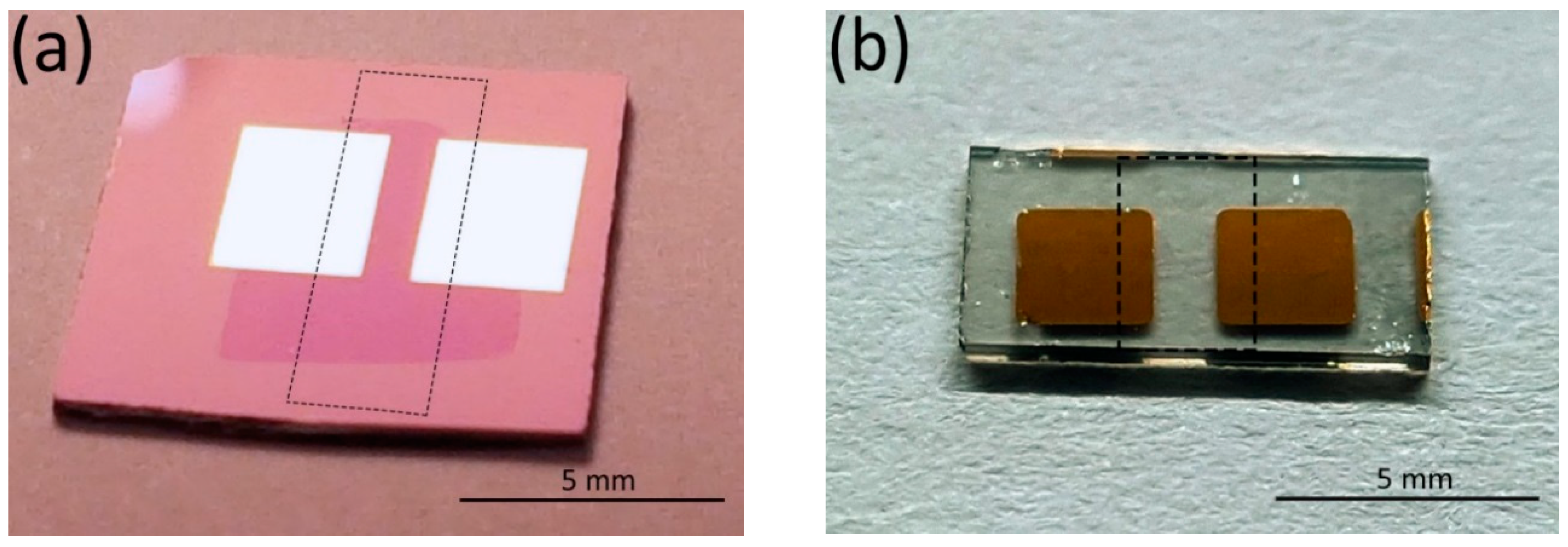
2. Materials and Methods

Chemical vapour deposited (CVD) graphene (CVDG) was grown on a commercial, 25-µm-thick polycrystalline copper foil in a home-built CVD reactor. The graphene film was transferred onto a Si/SiO2 substrate carrying Au (60 nm) electrodes, deposited through a shadow mask via magnetron sputtering (Figure 1a). The graphene growth and transfer process is already thoroughly described in [15].
Large area epitaxial graphene (EG) was grown using a sublimation method on Si-terminated 4H-SiC (0001) substrates at 2000 °C in argon gas at a pressure of 1 bar [18]. Au (200 nm) contact pads were made using DC-sputtering on top of SiC/EG substrate.
In the PLD process, which is specified in [15], a ceramic V2O5 target was ablated using a KrF excimer laser at wavelength 248 nm and laser pulse energy density of 5.0 J/cm2 in the presence of 5 × 10⁻² mbar of O2. A total of 120 laser pulses was used for V2O5 layer deposition. Sensor substrates were kept at the room temperature during deposition. For comparison, another V2O5 layer was deposited onto a fused quartz substrate while keeping the experimental conditions exactly the same so that in the following, the mass thickness of deposited layer can be evaluated in the x-ray fluorescence (XRF) measurement.
The CVD graphene was probed using a micro-Raman spectroscopic system (Renishaw, inVia, Gloucestershire, UK) at the excitation wavelength of 514 nm, with a spot diameter of ≈1 μm and incident radiant power of 1 mW. In case of epitaxial SiC graphene 17 mW of 532 nm laser light was focussed to a spot with diameter of ≈0.9 μm. For the V2O5 decorated epitaxial graphene sample, the laser power was reduced to 1 mW in order to diminish the risk of surface damage. The Raman spectrum of graphene on SiC was obtained after subtracting a reference Raman spectrum of pure carrier material 4H-SiC (0001) from the graphene spectrum.
The amount of vanadium in the deposited layer was assessed with X-ray fluorescence method, and the oxidation state of deposited vanadium was determined by X-ray photoelectron spectroscopy, as described earlier [15].
Gas sensitivity was measured at room temperature in a 7 cm3 stainless steel sample chamber, equipped with a gas mixing system, which is more thoroughly described in [19]. The voltage applied to the electrodes was either 100 mV or 500 mV in the cases of CVD graphene and epitaxial graphene samples, respectively. The neat gases or mixtures used in our measurements were N2, O2, CO/N2, NO2/N2, SO2/N2, O2/N2 and NH3/N2, all 99.999% pure. All used gases and mixtures were of certified composition from AGA (The Linde Group, Estonian branch, Tallinn, Estonia). A gas mixture of 10% O2 + 90% N2 was flown through a UV lamp ozoniser for O3 production, and the resulting O3 concentration was monitored using an ozone analyser (model 430, Teledyne API, San Diego, CA, USA). The gas flow through the sample chamber was kept constant at 200 sccm. The nominal relative humidity of the testing gas was regulated between 0 and 50% during the measurements. During the experiments with UV light excitation, the 365 nm light intensity on the sample was ≈15 mW/cm2.

3. Results

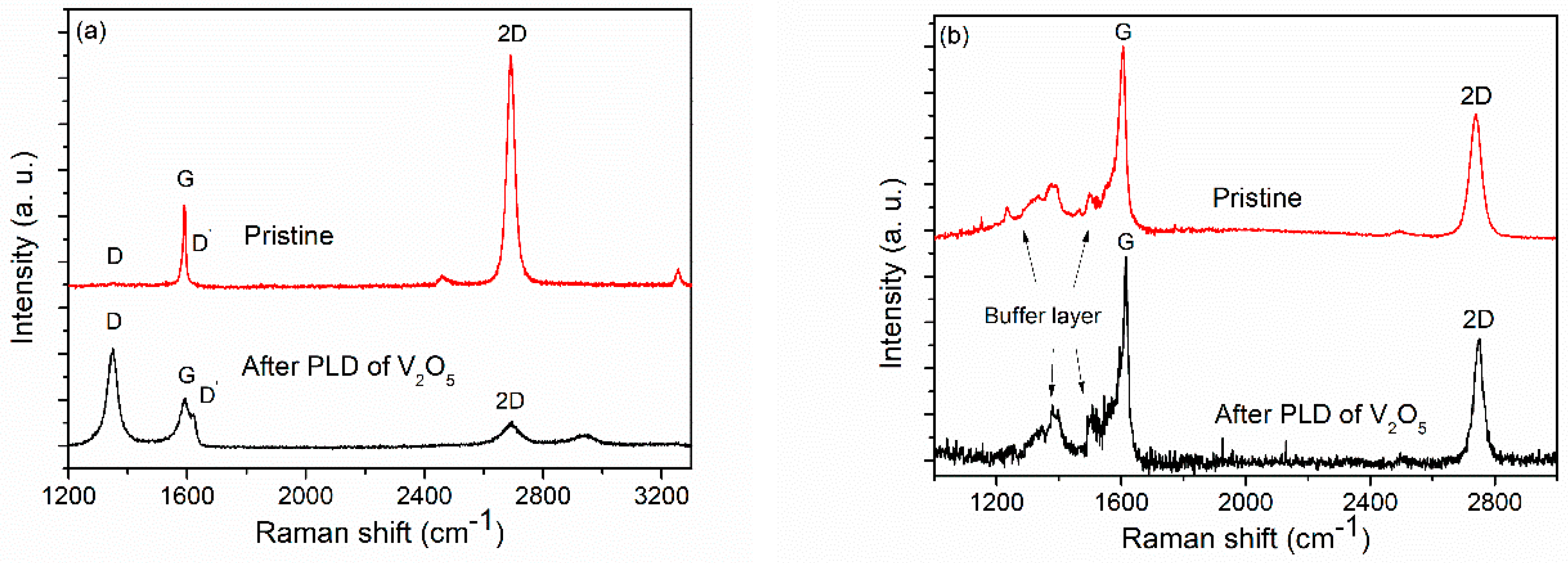
3.1. Characterization of Sensor Material Structure and Composition

Scanning electron microscope (SEM) images are displayed in Figure 2 for CVD and epitaxial graphene surfaces before and after the PLD of V2O5. The features appearing darker in the SEM of CVD graphene (Figure 2a,b) are typical for transferred CVD graphene. It seems that graphene follows the uneven surface topography of polycrystalline Cu foil used in the synthesis; some of the details are possibly wrinkles formed during the graphene transfer. The surface of pristine epitaxial graphene sample in Figure 2c is typical for graphene grown on a nominally single crystalline, on-axis, 4H-SiC substrate. It is characterized by wide terraces, which are due to the step-bunching of the SiC substrate surface that occurs during the high temperature growth [20]. Laser deposited nanostructured material could be distinguished in the SEM pictures of CVD (Figure 2b) and epitaxial (Figure 2d) graphene samples as numerous irregular dots and patches.
The Raman scattering cross section of graphene was remarkably large, owing to phenomena related to resonance enhancement, and was highly useful for structure characterisation. In the case of CVD graphene, the thick supporting material Si/SiO2 contributed surprisingly little to scattering intensity, so that the graphene spectrum could easily be separated. Figure 3a displays a typical Raman spectrum of pristine CVD graphene, recorded in the gap between the electrodes of the gas sensor setup. The G and 2D band peaks at ≈1590 cm−1 and ≈2690 cm−1, and have full-width at half-maximum (FWHM) of 11 cm−1 and 29 cm−1, respectively. These parameters, together with the 2D to G peak intensity ratio of approximately one to three, corresponded to a single layer of graphene [21]. Missing the defect-related D peak, usually located at ≈1350 cm−1, is an indication of low defect density in the pristine CVD graphene sample [21,22]. However, following PLD of V2O5 onto graphene, prominent defect-related D and D´ bands emerged in the Raman spectrum, and, at the same time, the G and 2D bands decreased in height (see Figure 3a).
Figure 3b compares Raman spectra for the as-grown epitaxial graphene (SiC/EG) and the same decorated with V2O5. The scattering onset beginning at about 1280 cm−1 and extending into the G-peak region originates from the interfacial “buffer” layer between the graphene and SiC substrate, and despite overlap with the expected D peak, is not related to defects [23]. Since these features extended up to the position of the G peak, they also gave rise to an apparent increase in G peak intensity, so that the G line appeared to have a higher intensity than the 2D band, even for monolayer graphene on SiC [8].
Remarkably, for EG on a SiC substrate, the typical Raman peaks indicated that graphene remained intact after the standard PLD treatment. The only noticeable difference between the spectra was higher signal to noise ratio in SiC/EG/V2O5 due to the lower laser power used, and a slight narrowing and blue-shift of the G and 2D peaks, which can originate from several factors influencing the Raman bands of SiC/EG. Mechanical strain was the major cause affecting the positions of characteristic epitaxial graphene Raman peaks [24], compared to exfoliated graphene. Strain inhomogeneity is recognized for causing variations of peak positions and widths, even in the Raman spectra taken from the same sample [25,26]. Change in graphene doping levels as a result of graphene-substrate interaction is known to influence the positions and widths of G and 2D bands of SiC/EG samples [24,27]. Charge transfer can also take place during graphene functionalisation with V2O5. The FWHM of the 2D peak in SiC/EG with V2O5 was 34.5 cm−1, which is characteristic for monolayer graphene.
The laser ablation plasma species have a broad kinetic energy distribution. A noticeable portion of these particles may have energy sufficient for creating point defects as a result of removal of C atoms from the graphene lattice (20 to 100 eV) [28]. As a consequence of laser deposition of V2O5 onto CVD graphene, the Raman lines assignable to point defects or imperfect graphene edges emerged in the spectrum (Figure 3a). However, according to the Raman spectra depicted in Figure 3b, there were no noticeable defect related lines, and thus no considerable increase of defectiveness in the SiC/EG/V2O5 sample.
The Raman spectrum of graphene and graphene related systems was fairly sensitive to structural disorder. The ratio of the D and G peaks ID/IG characterizes disorder induced by point defects [22,29,30]. However, the relationship between ID/IG and average distance between the point defects LD is non-monotonic and switches from a I(D)/I(G) ∝ LD2 type of dependence to a I(D)/I(G) ∝ 1/LD2 type at around LD ≈ 4 nm [30]. Because of the increased width of the G and D´ peaks of spectrum in Figure 3a, it is safe to conclude that we were in the region where LD < 4 nm. From the ratio ID/IG = 2.88, obtained from Figure 3a, the formulae given by Ferrari et al. [22] yields the average distance between point defects as being LD ≈ 2.3 nm, and the defect density nD of graphene as ≈6.1 × 1012 cm−2. Therefore, the initially pristine CVD graphene with very low defect density suffers damage during the PLD process, acquiring a high level of structural disorder. By contrast, according to Raman analysis, the PLD process did not noticeably increase the defectiveness of the epitaxial graphene sample. The conclusions about the influence of PLD reached on the basis of Raman spectra were supported by the electrical conductivity of samples. The conductivity of the CVD graphene sample, which had the Raman spectrum depicted in Figure 3a, decreased by 4 times after the PLD process, plausibly because of the decreased charge carrier mobility of the defective graphene lattice. The conductivity of the epitaxial graphene sample was unchanged after the PLD, which implies much less of a destructive influence.
The amount and oxidation state of vanadium deposited with exactly the same PLD procedure was investigated in our previous work by means of X-ray fluorescence (XRF) and X-ray photoelectron spectroscopy (XPS) [15]. In accordance with the vanadium XPS spectrum and the measured mass thickness of deposited V, the material deposited on graphene was predominately V2O5 with an average thickness of about 0.6 nm.

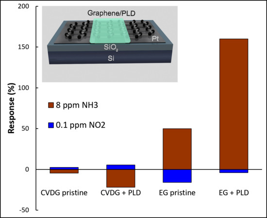
3.2. The Role of Sensor Functionalisation

All sensor measurements in this work were done at room temperature (293–298 K), mainly under continuous excitation with ultraviolet (UV) light (λ = 365 nm), except for several experiments performed without UV exposure for comparison. The influence of graphene functionalisation on the response to NH3 gas is illustrated for CVD and epitaxial graphene sensors in Figure 4. The response is defined as a relative change of conductance G: S = (GG0)/G0, where G0 is the conductance in synthetic air.
The conductivity of CVD graphene and epitaxial graphene sensors changes to the opposite direction after introducing NH3 into the test chamber. This was in accordance with the most prominent difference between Si/SiO2/CVDG and SiC/EG given their doping pattern in terms of majority charge carriers, p and n, respectively. In general, CVD graphene exhibits p-type conductivity and gas response at normal atmospheric conditions, primarily because of chemical doping by adsorbed oxygen and water molecules [31,32], and possibly, due to interaction with ≡Si–O–H groups on the oxidised silicon substrate. In the case of epitaxial graphene grown on the Si face of 4H-SiC (0001), however, electrons are most often the major carriers, because of charge transfer from the SiC substrate [33,34]. Bearing in mind that NH3 acts as a hole acceptor (electron donor) with respect to pristine graphene [1], the conductivity of CVD graphene is expected to decrease, and that of epitaxial graphene to increase, in accordance with observations. A different behaviour of EG without UV light (see the red curve in Figure 4b) is discussed in the next Section 3.3.
The electrical response dynamics of a 2D chemiresistor follows the kinetics of adsorption and chemical processes taking place on the surface. In general, the time dependent gas response to NH3 and the subsequent recovery curves can be suitably fitted with double exponential functions that give much better approximation than single exponentials:
G ( t ) = G 0 + A 1 [ 1 e ( t t 0 ) t 1 ] + A 2 [ 1 e ( t t 0 ) t 2 ] ,
in Equation (1), G0 is the initial conductance and G(t) is the conductance at time t; and t0 is the initial moment of time, when the respective stepwise change in gas composition is introduced. The time-independent coefficients A1 and A2 are amplitudes of conductance change. Characteristic times t1 and t2 are inverse first-order rate constants for adsorption and desorption kinetics of gas molecules for pristine or V2O5 functionalised graphene [35].
In principle, a single exponential response corresponds to a single type of adsorption site available for molecules in the surface of graphene sensor. In contrast, the double exponential response (Equation (1)) would describe the situation where two sites with different adsorption and desorption rate constants exist [35]. In addition, double-exponential response and recovery kinetics may originate from competitive adsorption of different gas species, besides NH3. For instance, H2O and O2 are known to readily adsorb on graphene surface and influence the electrical properties of graphene [31,32].
Baseline of the sensor signal (that is, conductivity in synthetic air at some definite relative humidity level) is extremely stable. However, after exposing the sensor to some analyte gas, signal recovery to the baseline can take quite a long time, even when UV light excitation is used. This can be seen in Figure 4, where the sensor signal does not relax completely back to the baseline before the next NH3 gas injection. This was because the signal relaxation was not exponential but tended to be double-exponential, whereas one of the exponents had quite a large time constant. The reasons behind this slow recovery can be several and depend on the exact mechanism behind the sensor response: high desorption energy barrier of NH3 molecule, or slow re-oxidation of V2O4 to V2O5, or some slow charge balancing processes between graphene and substrate etc.
A slow response and recovery of the graphene-based gas senor signal is quite common in the literature [1,3,4,8]. It depends on the practical task at hand, but generally, the fast sensor response and recovery is preferred in applications. However, preliminary experiments in our lab have shown that there can be certain graphene/functionalising material combinations in which case the gas responses and recoveries can be considerably faster. In addition, using short heat pulses during sensor work or doping with precious metals and nanoparticles are other possibilities to speed up the processes.
The results depicted in Figure 4 and Table 1 and Table 2 clearly show that, as compared to the pristine sensors, the response to NH3 was considerably improved after functionalisation using PLD. The relative response amplitudes to 8 ppm NH3, under UV light excitation, increased from 5 to 22%, and from 50 to 160% for CVDG and EG samples, respectively. Further, much faster characteristic response times were measured on both types of sensors (Table 1 lines 1 and 4, Table 2 lines 1 and 4), but the improvement of response and recovery dynamics was more drastic for the CVDG sensor. The increase of the gas response amplitude probably arose from increased density of energetically favourable adsorption sites or/and increased charge transfer between the graphene/V2O5 system and NH3 adsorbate molecules [15]. Such an improvement can arise from the strong adsorption ability of NH3 on V2O5 and possible redox reactions on the surface of V2O5 [36,37]. Similarly, fairly good NH3 gas sensing properties of semiconducting V2O5 thin films have been demonstrated by Huotari et al. [38].

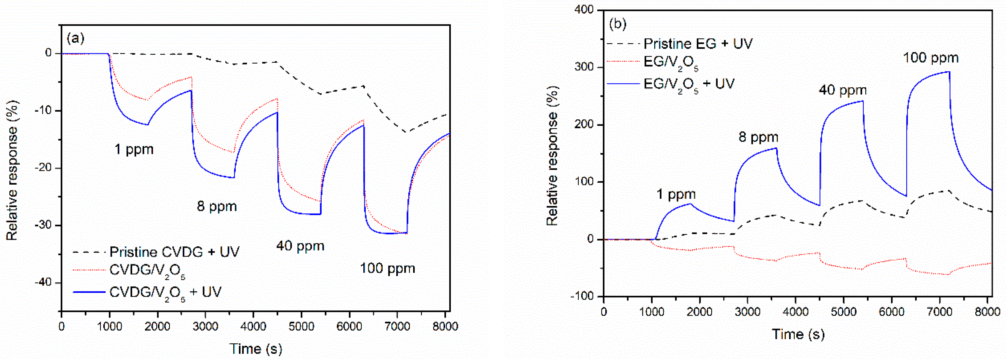
3.3. Effect of UV Excitation

Simultaneous exposure to UV light can enhance the sensing performance of graphene-based gas sensors drastically. By using UV irradiation, a considerably quicker response to tested gases, and also a faster recovery of the signal, has been reported [11,19,39]. This effect is likely a consequence of cleaning the surface from interfering or passivating gases. The results have been rationalised as photoinduced desorption of oxygen and water molecules, thereby vacating additional adsorption sites on graphene for the target gas. The effect of adsorption activation can be seen in the case of a CVD graphene sensor at lower gas concentrations where the response time and response amplitude improve considerably under UV light illumination (Figure 4a and Table 1). The recovery time of the CVDG sensor also shortened to some extent due to increased desorption.
In case of the EG sensor, the effect of UV light was particularly drastic, as the response to NH3 gas without UV light was characteristic of a p-type sensor (i.e., the conductivity decreased upon adding NH3), whilst it changed to the n-type response under the UV light. Previously, a switch from an n- to p-type response has been observed for epitaxial graphene gas sensors under increasing concentrations of NO2 [40]. The effect was explained in terms of withdrawal of electrons from EG by adsorption of electron-accepting molecular dopant NO2, which results in a lower concentration of free electrons, making the holes a major charge carrier. Besides water vapour and O2, which act as p-type dopants when adsorbing onto graphene in the ambient air [31,32], there may be yet undetermined adsorbing gases capable of strongly p-doping both the transferred CVD graphene and epitaxial graphene on SiC [41,42]. Therefore, the p-type response of an EG sensor sample is probably caused by adsorbed water vapour, O2 and other molecules, which can chemically p-dope graphene and cause n- to p-type switching of pristine graphene, as well as the EG/SiC/V2O5 system. As discussed before, the EG functionalisation with V2O5 did not influence the conductivity and defectiveness of epitaxial graphene samples, and is, therefore, probably not accompanied by a major change in electronic properties (mobility and concentration of charge carriers) of epitaxial graphene. Under the UV light exposure, the photo-activated desorption of molecules responsible for p-doping results in epitaxial graphene exhibiting n-type conductivity.

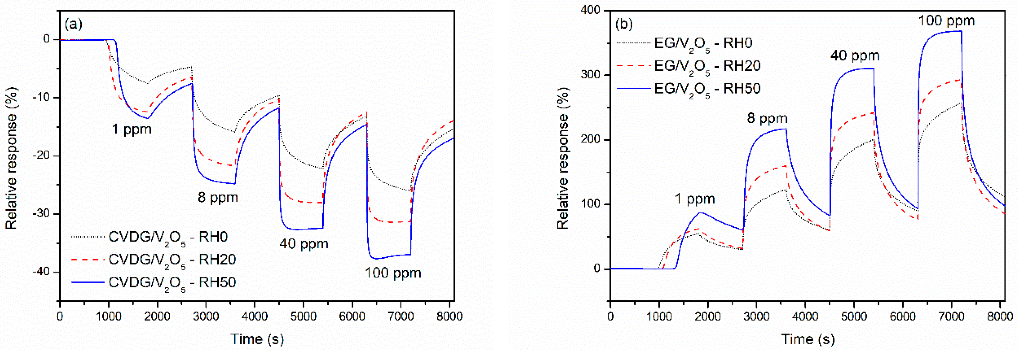
3.4. Influence of Humidity

In order to clarify the possible effect of varying humidity level on NH3 gas sensing properties, the measurements were carried out under variable relative humidity (RH%) levels of RH0, RH20 and RH50. The results are depicted in Figure 5. Clearly, the response time and amplitude improved with the increasing humidity level for both CVD and epitaxial graphene sensors. Under RH50, as compared to RH0 conditions, the characteristic response time t2 at 8 ppm NH3 decreased by 2.1 and 2.6 times for CVDG and EG sensors, respectively. At the same time, the response amplitude increased from 16% to 25% for CVDG, and from 131% to 216% for EG sensor. This clearly implies an important role of H2O in the NH3 adsorption mechanism on the surface of sensing layer.
The adsorption of ammonia on V2O5 has been thoroughly investigated to improve the catalytic reduction of NO2 in the presence of NH3, an important technology for detoxification of internal combustion engines exhausts. Two strongly bound species are typically observed as a result of the reaction of NH3 with V2O5 adsorption sites: one with the surface OH group (Brønsted acid site), forming a positively charged NH4+, and the other with the oxygen vacancy (Lewis acid site), forming a species, which is denoted as “coordinated NH3” [43]. Although a theoretical study conducted by Yin et al. [44] indicates that adsorption of NH3 takes place at both sites, adsorption at the Brønsted site is probably energetically more favourable than adsorption at Lewis site. According to Lin et al. [45], the number of Brønsted surface sites on V2O5 is directly related to the presence of water vapor. As a consequence of increasing H2O concentration in the system, a number of Lewis adsorption sites are converted to Brønsted sites (surface OH groups) by H2O adsorption on Lewis sites [45]. Therefore, a faster and larger response under humid measuring conditions of functionalised graphene sensor indicates the favourable role of Brønsted-type adsorption sites over the Lewis-type sites in V2O5.

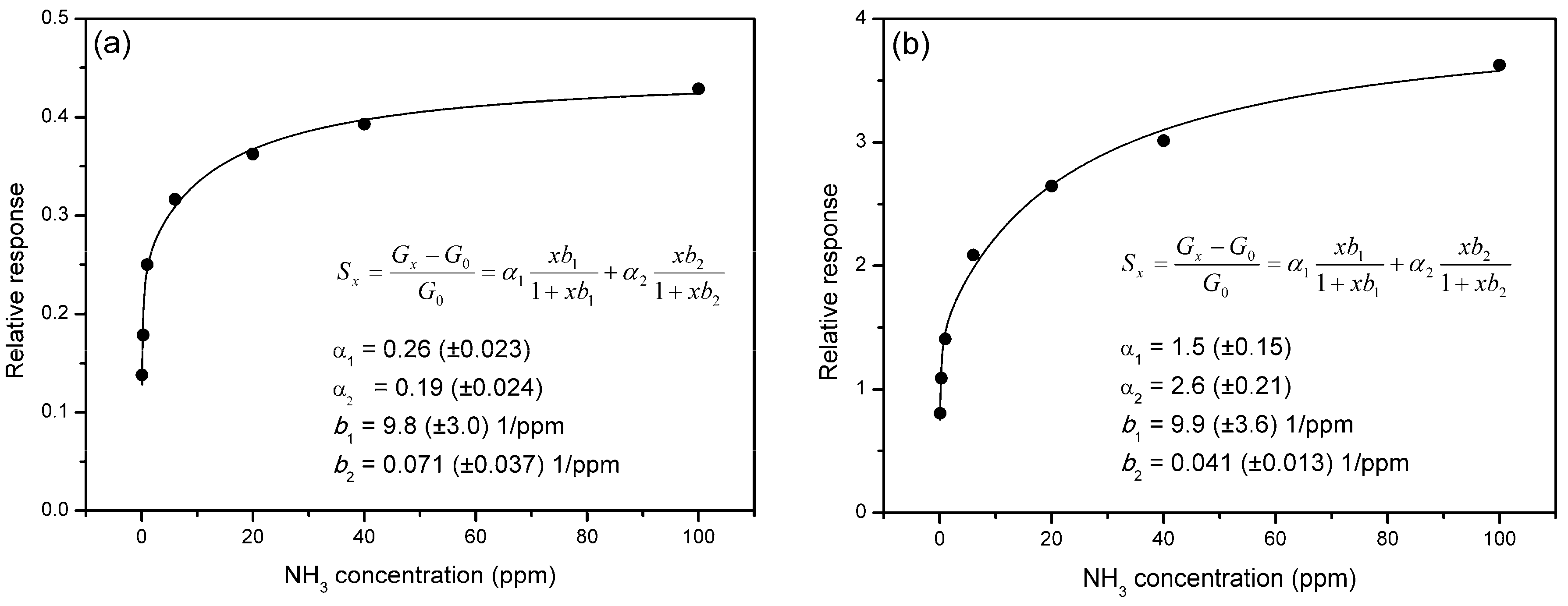
3.5. Langmuir Model Fitting of Sensor Response

In Figure 6, the stationary relative response of graphene sensors functionalised with V2O5 is plotted against NH3 concentration between 0.1 and 100 ppm. The response to NH3 gas in this concentration range was between 0.14 and 0.43 for the CVDG sensor and between 0.80 and 3.63 for the EG sensor. The dependence of responses on NH3 concentration followed a Langmuir-type ratiometric function. However, it turned out that stationary responses could not be fitted with a single-site Langmuir adsorption model, but closely followed a two-site Langmuir model [35]:
S x = G x G 0 G 0 = α 1 x b 1 1 + x b 1 + α 2 x b 2 1 + x b 2 ,
where b1 and b2 are the affinity constants, and α1 and α2 are transduction coefficients, according to the simplified transducer function model for CVD graphene oxygen sensor in [35]. Of course, Equation (2) presumes that transduction coefficients do not depend on the surface coverage, i.e., the change of carrier density and mobility per unit change of coverage does not depend on coverage itself, assuming no screening effects or interactions between adsorbates [35]. The Langmuir function is applicable in the case of a homogenous surface with a single type of adsorption site with a definite adsorption energy. In this case, only the first half of Equation (2) is needed to describe the system. If one assumes the existence of two sites for gas adsorption with different energetic parameters, the model leads to Equation (2), which was used for fitting the experimental data. Fitting of data points in Figure 6 yielded the following values of parameters for the CVDG sensor: α1 = 0.26 (±0.023), α2 = 0.19 (±0.024), b1 = 9.8 (±3.0) 1/ppm, b2 = 0.071 (±0.037) 1/ppm; and the following parameters for the EG sensor: α1 = 1.5 (±0.15), α2 = 2.6 (±0.21), b1 = 9.9 (±3.6) 1/ppm, b2 = 0.041 (±0.013) 1/ppm.
Here, two important aspects are to be noted:
(a)
The transduction coefficients α1 and α2 were both much smaller in case of the CVD graphene sensor, which means either a smaller influence of gas adsorption on the conductivity, or a lower concentration of total active adsorption sites.
(b)
The values of corresponding affinity constants b1 and b2 were very close for both types of graphene sensors, which mean that rate constants for adsorption and desorption were similar for both types of functionalised graphene.
The point (a) is discussed further below. The last deduction is also clearly evident from data in Table 1 and Table 2 where it can be seen that characteristic times for the response and recovery were nearly the same for functionalised graphene sensors. This means that the type of defects and their adsorption energies were almost the same in the case of functionalised CVD and epitaxial graphene. In addition, the ratios α12 amounted to 1.4 and 0.58 for CVDG and EG sensors, respectively, which means that the proportion of high affinity sites was considerably higher in the case of the CVD graphene or that their influence on the sensor’s conductivity was proportionally lower in the case of the EG sensor.

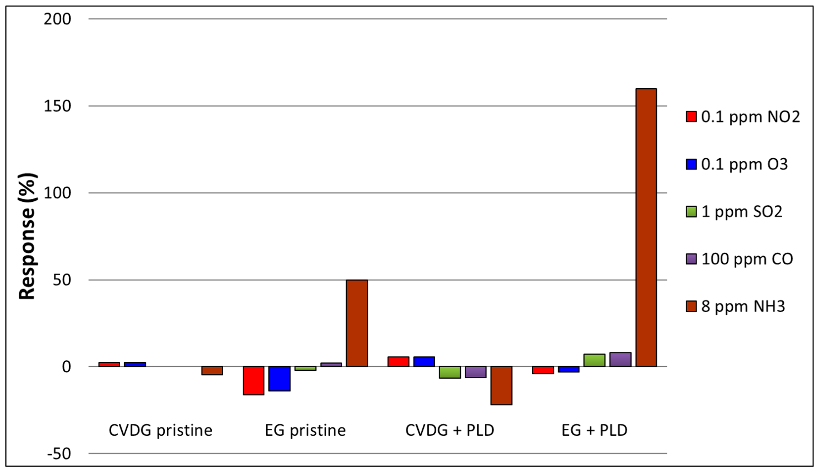
3.6. Sensor Selectivity

In sensors built on a single layer graphene and other graphene-related materials, the sensitivity to strongly oxidizing NO2 gas is generally much higher than that to other gases from the list of important gaseous pollutants. Strong binding and large charge transfer undoubtedly accompany NO2 molecule adsorption on either pristine, highly defective, or doped graphene [2,3]. Still, theoretical considerations indicate that the reducing NH3 molecule can also interact strongly with defects or dopants in graphene, and this is confirmed to a certain extent by experimental evidence [3].
The responses of our CVD and epitaxial graphene sensor devices to several polluting gases are compared in Figure 7. We have already shown previously [15] that single layer CVD graphene functionalised with laser deposited V2O5 was considerably more selective to NH3 gas, rather than to NO2. PLD functionalisation of CVD graphene with Ag or ZrO2, in the contrary, resulted in a higher selective response towards NO2 gas [15]. The same tendency is also seen in Figure 7. Compared to the pristine sensors of both types of graphene, the response to NH3 gas increased considerably through functionalisation, and at the same time, the response to NO2 gas diminished, as in the case of EG, or increased only slightly, as in the case of CVDG.
The functionalisation with V2O5 also enhanced the response to CO and SO2 gases for both types of sensors. Reactions to O3 and NO2 gases were quite similar, which was expected, as both molecules are strongly oxidizing, with electron affinity (EA) of 2.1028 eV and 2.273 eV [46], respectively.

4. Discussion

Pulsed laser deposition (PLD) was used to create a sub-nanometer V2O5 layer on graphene samples, either synthesized using chemical vapour deposition (CVD graphene) and transferred to Si/SiO2, or epitaxial graphene on a SiC substrate. Raman analysis showed that the defectiveness of CVD graphene increased drastically following PLD, which is an expected result of bombardment with a high energy PLD plasma species. By contrast, the defect concentration of epitaxial graphene is not affected by an identical PLD process, which implies considerable resilience against defect creation. This finding is in accordance with the fact that the electrical conductivity of the SiC/EG sample did not change after the PLD of V2O5, while the conductivity of CVD graphene was substantially reduced.
As a possible explanation, we refer to self-healing phenomenon, i.e., reknitting of holes in the graphene during annealing at elevated temperatures [47], or even at room temperature under scanning electron beam [48]. Chen et al. [47] reported the partial recovery of Raman peaks and conductivity of the damaged graphene after annealing at 300 °C. We have also noticed partial recovery of the structure and conductivity of PLD treated CVD graphene samples after keeping them in vacuum at 150 °C. By contrast, at room temperature, the healing process is unlikely, resulting in severe defect creation in case of CVD graphene on Si/SiO2 substrate subject to PLD plasma.
Since the self-healing does not occur at 295 K, the negligible deterioration of structure and conductivity in the epitaxial graphene could rather mean considerably higher energy threshold for defect creation. The substrate supporting graphene can play a major role under a flux of highly energetic particles (≈1 MeV), in which case the majority of defects found in graphene are created using the backscattered ions or sputtered atoms from the substrate [49]. For impinging particles having considerably lower energy (up to 10 keV), the indirect defect creation mechanism may still predominate over direct damage in the case of supported graphene [50]. The damage threshold energy was much higher for supported graphene, as compared to suspended graphene [49,50].
Bearing in mind a much tighter graphene-to-support contact, resilience to plasma treatment of SiC/EG can be understood. The transition layer between the sp2 graphene and the sp3 bulk material in SiC/EG is covalently bound to SiC substrate and serves as a template during epitaxial growth of graphene on the Si face of SiC [20]. Thus, every atom of growing graphene is in an optimal position, and the graphene closely follows the substrate surface topography. On the other hand, CVDG transferred onto the Si/SiO2 surface can be quasi-suspended, with the van der Waals contact area probably much less than 100%. In other words, the potential for C atoms in epi-graphene has a much deeper minimum. Thus, in qualitative terms, SiC/EG is more durable under the bombardment with high velocity particles, owing to the stronger bond of the graphene sheet with the underling substrate.
A large enhancement of response to the reducing NH3 gas was achieved for both types of graphene sensors as a result of laser-deposited, thin V2O5 functionalising layer. The magnitude of the relative response of SiC/EG/V2O5 sensor was particularly noteworthy, for instance, amounting to 310% for 40 ppm NH3 at 50% relative humidity. The stationary gas response to the lowest NH3 concentration that could be tested, 0.1 ppm, was 14% and 80% at 20% relative humidity for CVDG and SiC/EG, respectively.
Perfect graphene is relatively inert with respect to chemisorption due to the negligible amount of dangling bonds and a lack of charged atoms on the surface [2,3]. Pristine graphene samples always contain, often unidentified, dopant atoms, defects and organic residues left from the polymer film. Some of these species may even be beneficial when considering the gas adsorption ability. The defects or dopant atoms in the graphene lattice, or atom clusters on graphene surface, can promote adsorption of gaseous pollutants. The effect of adsorption on electric characteristics is also modified [7,51]. Some gas sensitivity, usually in conjunction with very slow sensor recovery at room temperature, is characteristic of pristine graphene, indicating the presence of binding sites with high adsorption energy, occurring at a low density in CVD [3], epitaxial [4], and exfoliated graphene [1]. During functionalisation using PLD, a high number of point defects is formed by bombardment with high energy atoms in the case of CVD graphene. More importantly, the system is modified by adding functionalising oxide material [6,15]. Basing on results shown in Figure 4 and data in Table 1 and Table 2, an increased response and faster dynamics was obvious for functionalised sensors. Functionalised graphene has a higher density of gas adsorption sites with suitable binding energies, resulting in a larger and faster sensor response.
The response dependence on NH3 concentration is well approximated using a two-site Langmuir model, which yielded two affinity constants b1 and b2, with a difference by two orders of magnitude in both graphenes. However, the corresponding affinities were similar in both instances, showing that CVDG/V2O5 and SiC/EG/V2O5 sensors have sites with similar adsorption energies, i.e., the adsorption sites belonged to the functionalising V2O5 layer, and did not depend on the type of the graphene. The comparable NH3 adsorption affinities of both types of graphene would produce similar responses and recovery times of sensors (Table 1 and Table 2).
We were able to advance only tentative explanations about the elementary mechanisms, based on NH3 adsorption and conversion processes on V2O5 surface that are quite extensively covered in the literature on heterogeneous catalysis (see, for example, [36,37]). Among our main findings is the biphasic response kinetics and the amplitude enhancement in the presence of humidity. The possible surface redox reactions taking place in case of graphene/V2O5 sensor were previously discussed in [15]. Broadly speaking, V5+ was perhaps reduced to V4+ by ammonia and the polaron thus formed migrated in the V2O5 lattice and finally reached graphene. The experiments potentially allowing one to distinguish between different mechanisms of graphene conductivity change, as well as to establish the chemical reactions between NH3 and O2 on the surface are in progress.
As can be observed form the measurement results in Figure 5 and Figure 7, both pristine and functionalised epitaxial graphene gas sensors had nearly ten times higher relative response to NH3 gas than the corresponding CVD graphene sensors. This was reflected in the transduction coefficients α1 and α2 in the Langmuir model (Equation (2)), which were both much smaller in the case of CVD graphene. The major part of the more sensitive nature of EG was most probably related to the particular feature of gas sensing mechanism of the graphene. It was found by Schedin et al. [1] that charge transfer is the main mechanism of gas sensitivity in the case of exfoliated graphene sheet placed on top of the Si/SiO2 substrate, e.g., the gas adsorption solely modified the concentration of free charge carriers in graphene without changing their mobility. If we assume the same for our sensors, then the change of carrier mobility, caused by the NH3 adsorption was smaller than the effect of carrier concentration, and the gas response amplitude S is determined by a relative change of charge carrier numbers Δn/n0 [35]:
S = G G 0 G 0 = n ˜ Δ θ n 0 ,
where Δ θ is the fractional coverage change for the adsorbed species, n0 is the carrier concentration in the absence of adsorbate gas, and the constant n ˜ characterises the change of carrier density per unit change of coverage.
The amount of charge transferred per unit change of coverage (i.e., density of adsorption sites and charge transferred per site) was similar for both types of graphene sensors. It follows that the lower initial concentration of carriers n0 of the graphene would correspond to a stronger gas response, and vice versa. In sensors used in this work, the conductivity of pristine CVD graphene was about 15 times higher than that for epitaxial graphene. Given that typical carrier mobility is not very different for pristine samples of CVDG and EG, 1000–3000 and ≈1000 cm2·V−1·s−1, respectively, the charge carrier density in CVDG should be about one order of magnitude higher than that in EG. This conclusion is well supported by the literature data on the typical electronic doping levels of SiC/EG and Si/SiO2/CVDG.
Both epitaxial graphene grown on Si-terminated 4H-SiC (0001) and CVD graphene transferred to Si/SiO2 are typically highly doped, owing to interactions with the underlying substrate or surface adsorbates, i.e., water, oxygen and other adsorbate molecules [41,42]. Room temperature charge carrier concentration, due to doping effects are typically near 1012 cm−2 in the case of SiC/EG [41,52,53] and near 1013 cm−2 in the case of Si/SiO2/CVDG [42]. Since adsorption sites seem to be energetically similar for both types of sensors, the difference in the response magnitudes to NH3 (by an order of magnitude) probably arose as a result of the lower initial doping level of SiC/EG. In other words, the Fermi energy level being closer to the Dirac point allowed for higher sensitivity to chemical doping, induced by adsorbing NH3 molecules. The proximity of the Fermi level to a Dirac point in SiC/EG was supported by the fact that under UV light, which is capable of removing the major atmospheric dopants, the response of EG-based sensors switched from p- to n-type.

5. Conclusions

The functionalisation of CVD-grown and epitaxial graphene with V2O5 enhanced the response and improved the selectivity of chemiresistive sensors with respect to ammonia. The analysis of sensor kinetics implied the presence of similar adsorption sites in both kinds on functionalised graphenes, indicating that the deposited V2O5 nanophase was a predominating NH3 receptor. The difference in the magnitudes of relative gas response was a result of different charge carrier type and concentration of graphene samples. Epitaxial graphene on SiC was remarkably resistant to PLD plasma. The signals of sensors on SiC/EG platform were larger, faster and more reversible than those for CVD graphene. However, the transferability of CVD graphene onto almost any surface could be of great value.
Graphene is almost ideally suited as a signal transducer material in conductive sensors. Since pristine graphene is a relatively weak and non-specific adsorbent, the progress will essentially depend on the quality of receptor function created by means of functionalisation. Only time will tell whether graphene is superior to other categories of thin conductors, such as nanoSMOX (semiconducting metal oxides) and TMD (transition metal dichalcogenides) [54,55,56].

Author Contributions

Conceptualization, M.K., R.J., H.A., J.E. and R.Y.; methodology, R.J., H.A., I.R., M.K.; validation, M.K., T.K. and A.B.; formal analysis, M.K. and T.K.; investigation, M.K. and T.K.; resources, J.E. and R.Y.; writing—original draft preparation, M.K. and I.R.; writing—review and editing, M.K., J.E., R.Y., R.J., H.A., I.R., T.K., T.A., A.B.; visualisation, M.K.; supervision, R.J. and H.A.; project administration, R.J. and H.A.; funding acquisition, H.A. and R.J.

Funding

This project has received funding from the European Union’s Horizon 2020 research and innovation program under the grant agreement No 785219 and by the EU through the European Regional Development Fund (TK141 “Advanced materials and high-technology devices for energy recuperation systems”). The work was also supported by institutional research funds IUT34-27 and IUT2-24 of the Estonian Ministry of Education and Science. J.E. and R.Y. would like to thank financial support from the Swedish Foundation for Strategic Research (SSF), through the grants GMT14-0077 and RMA15-024.

Acknowledgments

The authors would like to thank Aarne Kasikov for sensor electrode preparation, Helina Seemen and Jekaterina Kozlova for SEM imaging, and Ahti Niilisk for help with Raman measurements.

Conflicts of Interest

The authors declare no conflict of interest. The funders had no role in the design of the study; in the collection, analysis, or interpretation of data; in the writing of the manuscript, or in the decision to publish the results.

References

  1. Schedin, F.; Geim, A.K.; Morozov, S.V.; Hill, E.W.; Blake, P.; Katsnelson, M.I.; Novoselov, K.S. Detection of individual gas molecules adsorbed on graphene. Nat. Mater. 2007, 6, 652–655. [Google Scholar] [CrossRef] [PubMed] [Green Version]
  2. Zhang, Y.-H.; Chen, Y.-B.; Zhou, K.-G.; Liu, C.-H.; Zeng, J.; Zhang, H.-L.; Peng, Y. Improving gas sensing properties of graphene by introducing dopants and defects: A first-principles study. Nanotechnology 2009, 20, 185504. [Google Scholar] [CrossRef] [PubMed]
  3. Lee, G.; Yang, G.; Cho, A.; Han, J.W.; Kim, J. Defect-engineered graphene chemical sensors with ultrahigh sensitivity. Phys. Chem. Chem. Phys. 2016, 18, 14198–14204. [Google Scholar] [CrossRef] [PubMed]
  4. Eriksson, J.; Puglisi, D.; Kang, Y.H.; Yakimova, R.; Lloyd Spetz, A. Adjusting the electronic properties and gas reactivity of epitaxial graphene by thin surface metallization. Phys. B Condens. Matter 2014, 439, 105–108. [Google Scholar] [CrossRef] [Green Version]
  5. Zhao, M.; Dong, F.; Yan, L.; Xu, L.; Zhang, X.; Chen, P.; Song, Z.; Chu, W. High efficiency room temperature detection of NO2 gas based on ultrathin metal/graphene devices. RSC Adv. 2016, 6, 84082–84089. [Google Scholar] [CrossRef]
  6. Kodu, M.; Berholts, A.; Kahro, T.; Avarmaa, T.; Kasikov, A.; Niilisk, A.; Alles, H.; Jaaniso, R. Highly sensitive NO2 sensors by pulsed laser deposition on graphene. Appl. Phys. Lett. 2016, 109, 113108. [Google Scholar] [CrossRef]
  7. Zhang, J.; Zhao, C.; Hu, P.A.; Fu, Y.Q.; Wang, Z.; Cao, W.; Yang, B.; Placido, F. A UV light enhanced TiO2/graphene device for oxygen sensing at room temperature. RSC Adv. 2013, 3, 22185–22190. [Google Scholar] [CrossRef]
  8. Rodner, M.; Bahonjic, J.; Mathisen, M.; Gunnarsson, R.; Ekeroth, S.; Helmersson, U.; Ivanov, I.G.; Yakimova, R.; Eriksson, J. Performance tuning of gas sensors based on epitaxial graphene on silicon carbide. Mater. Design 2018, 153, 153–158. [Google Scholar] [CrossRef]
  9. Mu, H.; Wang, K.; Xie, H. Effects of the fabrication temperature and oxygen flux on the properties and nitrogen dioxide sensitivity of the tin oxides-tin/graphene hybrid sensor. J. Mater. Res. 2016, 31, 1993–2003. [Google Scholar] [CrossRef]
  10. Eason, R. (Ed.) Pulsed Laser Deposition of Thin Films: Applications-Led Growth of Functional Materials; Wiley-Interscience (Online Service): Hoboken, NJ, USA, 2006; ISBN 9780470052129. [Google Scholar]
  11. Chen, G.; Paronyan, T.M.; Harutyunyan, A.R. Sub-ppt gas detection with pristine graphene. Appl. Phys. Lett. 2012, 101, 053119. [Google Scholar] [CrossRef] [Green Version]
  12. Novikov, S.; Lebedeva, N.; Satrapinski, A.; Walden, J.; Davydov, V.; Lebedev, A. Graphene based sensor for environmental monitoring of NO2. Sens. Actuators B Chem. 2016, 236, 1054–1060. [Google Scholar] [CrossRef]
  13. Eriksson, J.; Puglisi, D.; Strandqvist, C.; Gunnarsson, R.; Ekeroth, S.; Ivanov, I.G.; Helmersson, U.; Uvdal, K.; Yakimova, R.; Lloyd Spetz, A. Modified epitaxial graphene on SiC for extremely sensitive and selective gas sensors. Mater. Sci. Forum 2016, 858, 1145–1148. [Google Scholar] [CrossRef]
  14. Gruber, M.; Hermann, K. Elementary steps of the catalytic NOx reduction with NH3: Cluster studies on reactant adsorption at vanadium oxide substrate. J. Chem. Phys. 2013, 138, 094704. [Google Scholar] [CrossRef] [PubMed]
  15. Kodu, M.; Berholts, A.; Kahro, T.; Kook, M.; Ritslaid, P.; Seemen, H.; Avarmaa, T.; Alles, H.; Jaaniso, R. Graphene functionalised by laser-ablated V2O5 for a highly sensitive NH3 sensor. Beilstein J. Nanotechnol. 2017, 8, 571–578. [Google Scholar] [CrossRef] [PubMed]
  16. Jaaniso, R.; Tan, O.K. (Eds.) Semiconductor Gas Sensors; Woodhead Publ.: Cambridge, UK, 2013; ISBN 9780857098665. [Google Scholar]
  17. Kodu, M.; Berholts, A.; Kahro, T.; Eriksson, J.; Yakimova, R.; Avarmaa, T.; Renge, I.; Alles, H.; Jaaniso, R. Highly sensitive NH3 sensors using CVD and epitaxial graphene functionalised with vanadium(V) oxide: A comparative study. Proceedings 2018, 2, 854. [Google Scholar] [CrossRef]
  18. Yakimova, R.; Virojanadara, C.; Gogova, D.; Syväjärvi, M.; Siche, D.; Larsson, K.; Johansson, L.I. Analysis of the formation conditions for large area epitaxial graphene on SiC substrates. Mater. Sci. Forum 2010, 645–648, 565–568. [Google Scholar] [CrossRef]
  19. Berholts, A.; Kahro, T.; Floren, A.; Alles, H.; Jaaniso, R. Photo-activated oxygen sensitivity of graphene at room temperature. Appl. Phys. Lett. 2014, 105, 162111. [Google Scholar] [CrossRef]
  20. Yazdi, G.R.; Iakimov, T.; Yakimova, R. Epitaxial graphene on SiC: A review of growth and characterization. Crystals 2016, 6, 53. [Google Scholar] [CrossRef]
  21. Ferrari, A.C.; Meyer, J.C.; Scardaci, V.; Casiraghi, C.; Lazzeri, M.; Mauri, F.; Piscanec, S.; Jiang, D.; Novoselov, K.S.; Roth, S.; et al. Raman spectrum of graphene and graphene layers. Phys. Rev. Lett. 2006, 97, 1–4. [Google Scholar] [CrossRef] [PubMed]
  22. Ferrari, A.C.; Basko, D.M. Raman spectroscopy as a versatile tool for studying the properties of graphene. Nat. Nanotechnol. 2013, 8, 235–246. [Google Scholar] [CrossRef] [PubMed] [Green Version]
  23. Lee, D.S.; Riedl, C.; Krauss, B.; von Klitzing, K.; Starke, U.; Smet, J.H. Raman spectra of epitaxial graphene on SiC and of epitaxial graphene transferred to SiO2. Nano Lett. 2008, 8, 4320–4325. [Google Scholar] [CrossRef] [PubMed]
  24. Bouhafs, C.; Zakharov, A.A.; Ivanov, I.G.; Giannazzo, F.; Eriksson, J.; Stanishev, V.; Kühne, P.; Iakimov, T.; Hofmann, T.; Schubert, M.; et al. Multi-scale investigation of interface properties, stacking order and decoupling of few layer graphene on C-face 4H-SiC. Carbon 2017, 116, 722–732. [Google Scholar] [CrossRef]
  25. Röhrl, J.; Hundhausen, M.; Emtsev, K.V.; Seyller, T.; Graupner, R.; Ley, L. Raman spectra of epitaxial graphene on SiC (0001). Appl. Phys. Lett. 2008, 92, 201918. [Google Scholar] [CrossRef]
  26. Robinson, J.A.; Puls, C.P.; Staley, N.E.; Stitt, J.P.; Fanton, M.A.; Emtsev, K.V.; Seyller, T.; Liu, Y. Raman topography and strain uniformity of large-area epitaxial graphene. Nano Lett. 2009, 9, 964–968. [Google Scholar] [CrossRef] [PubMed]
  27. Das, A.; Pisana, S.; Chakraborty, B.; Piscanec, S.; Saha, S.K.; Waghmare, U.V.; Novoselov, K.S.; Krishnamurthy, H.R.; Geim, A.K.; Ferrari, A.C.; et al. Monitoring dopants by Raman scattering in an electrochemically top-gated graphene transistor. Nat. Nanotechnol. 2008, 3, 210–215. [Google Scholar] [CrossRef] [PubMed] [Green Version]
  28. Wang, H.; Wang, Q.; Cheng, Y.; Li, K.; Yao, Y.; Zhang, Q.; Dong, C.; Wang, P.; Schwingenschlögl, U.; Yang, W.; et al. Doping monolayer graphene with single atom substitutions. Nano Lett. 2012, 12, 141–144. [Google Scholar] [CrossRef] [PubMed]
  29. Ferrari, A.C.; Robertson, J. Interpretation of Raman spectra of disordered and amorphous carbon. Phys. Rev. B 2000, 61, 14095–14107. [Google Scholar] [CrossRef]
  30. Cançado, L.G.; Jorio, A.; Ferreira, E.H.M.; Stavale, F.; Achete, C.A.; Capaz, R.B.; Moutinho, M.V.O.; Lombardo, A.; Kulmala, T.S.; Ferrari, A.C. Quantifying defects in graphene via Raman spectroscopy at different excitation energies. Nano Lett. 2011, 11, 3190–3196. [Google Scholar] [CrossRef] [PubMed]
  31. Ryu, S.; Liu, L.; Berciaud, S.; Yu, Y.J.; Liu, H.; Kim, P.; Flynn, G.W.; Brus, L.E. Atmospheric oxygen binding and hole doping in deformed graphene on a SiO2 substrate. Nano Lett. 2010, 10, 4944–4951. [Google Scholar] [CrossRef] [PubMed]
  32. Yang, Y.; Brenner, K.; Murali, R. The influence of atmosphere on electrical transport in graphene. Carbon 2012, 50, 1727–1733. [Google Scholar] [CrossRef]
  33. Varchon, F.; Feng, R.; Hass, J.; Li, X.; Nguyen, B.N.; Naud, C.; Mallet, P.; Veuillen, J.Y.; Berger, C.; Conrad, E.H.; et al. Electronic structure of epitaxial graphene layers on SiC: Effect of the substrate. Phys. Rev. Lett. 2007, 99, 3–6. [Google Scholar] [CrossRef] [PubMed]
  34. Emtsev, K.V.; Bostwick, A.; Horn, K.; Jobst, J.; Kellogg, G.L.; Ley, L.; McChesney, J.L.; Ohta, T.; Reshanov, S.A.; Röhrl, J.; et al. Towards wafer-size graphene layers by atmospheric pressure graphitization of silicon carbide. Nat. Mater. 2009, 8, 203–207. [Google Scholar] [CrossRef] [PubMed] [Green Version]
  35. Jaaniso, R.; Kahro, T.; Kozlova, J.; Aarik, J.; Aarik, L.; Alles, H.; Floren, A.; Gerst, A.; Kasikov, A.; Niilisk, A.; et al. Temperature induced inversion of oxygen response in CVD graphene on SiO2. Sens. Actuators B Chem. 2014, 190, 1006–1013. [Google Scholar] [CrossRef]
  36. Sun, D.; Liu, Q.; Liu, Z.; Gui, G.; Huang, Z. Adsorption and oxidation of NH3 over V2O5/AC surface. Appl. Catal. B Environ. 2009, 92, 462–467. [Google Scholar] [CrossRef]
  37. Centeno, M.A.; Carrizosa, I.; Odriozola, J.A. NO–NH3 coadsorption on vanadia/titania catalysts: Determination of the reduction degree of vanadium. Appl. Catal. B Environ. 2001, 29, 307–314. [Google Scholar] [CrossRef]
  38. Huotari, J.; Bjorklund, R.; Lappalainen, J.; Lloyd Spetz, A. Pulsed laser deposited nanostructured vanadium oxide thin films characterized as ammonia sensors. Sens. Actuators B Chem. 2015, 217, 22–29. [Google Scholar] [CrossRef]
  39. Lin, J.; Zhong, J.; Kyle, J.R.; Penchev, M.; Ozkan, M.; Ozkan, C.S. Molecular absorption and photodesorption in pristine and functionalized large-area graphene layers. Nanotechnology 2011, 22, 355701. [Google Scholar] [CrossRef] [PubMed]
  40. Pearce, R.; Iakimov, T.; Andersson, M.; Hultman, L.; Spetz, A.L.; Yakimova, R. Epitaxially grown graphene based gas sensors for ultra sensitive NO2 detection. Sens. Actuators B Chem. 2011, 155, 451–455. [Google Scholar] [CrossRef]
  41. Panchal, V.; Giusca, C.E.; Lartsev, A.; Martin, N.A.; Cassidy, N.; Myers-Ward, R.L.; Gaskill, D.K.; Kazakova, O. Atmospheric doping effects in epitaxial graphene: Correlation of local and global electrical studies. 2D Materials 2016, 3, 8–11. [Google Scholar] [CrossRef]
  42. Melios, C.; Centeno, A.; Zurutuza, A.; Panchal, V.; Giusca, C.E.; Spencer, S.; Silva, S.R.P.; Kazakova, O. Effects of humidity on the electronic properties of graphene prepared by chemical vapour deposition. Carbon 2016, 103, 273–280. [Google Scholar] [CrossRef]
  43. Gruber, M.; Hermann, K. Elementary steps of the catalytic NOx reduction with NH3: Cluster studies on reaction paths and energetics at vanadium oxide substrate. J. Chem. Phys. 2013, 139, 244701. [Google Scholar] [CrossRef] [PubMed]
  44. Yin, X.; Han, H.; Gunji, I.; Endou, A.; Ammal, S.S.C.; Kubo, M.; Miyamoto, A. NH3 adsorption on the Brönsted and Lewis acid sites of V2O5 (010): A periodic density functional study. J. Phys. Chem. B 1999, 103, 4701–4706. [Google Scholar] [CrossRef]
  45. Lin, C.-H.; Bai, H. Adsorption behavior of moisture over a vanadia/titania catalyst: A study for the selective catalytic reduction process. Ind. Eng. Chem. Res. 2004, 43, 5983–5988. [Google Scholar] [CrossRef]
  46. Lide, D.R. (Ed.) CRC Handbook of Chemistry and Physics, 89th ed.; CRC Press: Boca Raton, FL, USA, 2008. [Google Scholar]
  47. Chen, J.; Shi, T.; Cai, T.; Xu, T.; Sun, L.; Wu, X.; Yu, D. Self healing of defected graphene. Appl. Phys. Lett. 2013, 102, 103107. [Google Scholar] [CrossRef]
  48. Zan, R.; Ramasse, Q.M.; Bangert, U.; Novoselov, K.S. Graphene reknits its holes. Nano. Lett. 2012, 12, 3936–3940. [Google Scholar] [CrossRef] [PubMed]
  49. Li, W.; Wang, X.; Zhang, X.; Zhao, S.; Duan, H.; Xue, J. Mechanism of the defect formation in supported graphene by energetic heavy ion irradiation: The substrate effect. Sci. Rep. 2015, 5, 1–6. [Google Scholar] [CrossRef] [PubMed]
  50. Zhao, S.; Xue, J.; Wang, Y.; Yan, S. Effect of SiO2 substrate on the irradiation-assisted manipulation of supported graphene: A molecular dynamics study. Nanotechnology 2012, 23, 285703. [Google Scholar] [CrossRef] [PubMed]
  51. Zhou, M.; Lu, Y.H.; Cai, Y.Q.; Zhang, C.; Feng, Y.P. Adsorption of gas molecules on transition metal embedded graphene: A search for high-performance graphene-based catalysts and gas sensors. Nanotechnology 2011, 22, 385502. [Google Scholar] [CrossRef] [PubMed]
  52. Tzalenchuk, A.; Lara-Avila, S.; Kalaboukhov, A.; Paolillo, S.; Syväjärvi, M.; Yakimova, R.; Kazakova, O.; Janssen, T.J.B.M.; Fal’ko, V.; Kubatkin, S. Towards a quantum resistance standard based on epitaxial graphene. Nat. Nanotechnol. 2010, 5, 186–189. [Google Scholar] [CrossRef] [PubMed] [Green Version]
  53. Eriksson, J.; Pearce, R.; Iakimov, T.; Virojanadara, C.; Gogova, D.; Andersson, M.; Syväjärvi, M.; Lloyd Spetz, A.; Yakimova, R. The influence of substrate morphology on thickness uniformity and unintentional doping of epitaxial graphene on SiC. Appl. Phys. Lett. 2012, 100, 241607. [Google Scholar] [CrossRef] [Green Version]
  54. Joshi, N.; Hayasaka, T.; Liu, Y.; Liu, H.; Oliveira, O.N.; Lin, L. A review on chemiresistive room temperature gas sensors based on metal oxide nanostructures, graphene and 2D transition metal dichalcogenides. Microchim. Acta 2018, 185, 213. [Google Scholar] [CrossRef] [PubMed]
  55. Liu, X.; Ma, T.; Pinna, N.; Zhang, J. Two-dimensional nanostructured materials for gas sensing. Adv. Funct. Mater. 2017, 27, 1702168. [Google Scholar] [CrossRef]
  56. Zhang, J.; Liu, X.; Neri, G.; Pinna, N. Nanostructured materials for room-temperature gas sensors. Adv. Mater. 2016, 28, 795–831. [Google Scholar] [CrossRef] [PubMed]
Figure 1. Photographs of gas sensor devices based on (a) PLD-functionalised CVD graphene on a Si/SiO2 substrate, and (b) epitaxial graphene on a SiC substrate. Gaps between the electrodes are 1 × 4 mm2 and 1 × 2 mm2 for CVD and epitaxial graphene, respectively. The CVD graphene sheet on top of electrodes appears as a darker pink area in (a) due to slightly different reflection properties. The areas of laser deposition of V2O5 are marked with dashed lines.
Sensors 19 00951 g001
Figure 2. SEM images of pristine and PLD-treated graphene surfaces: (a) pristine CVD graphene, (b) CVD graphene functionalised with V2O5, (c) pristine epitaxial graphene on SiC and (d) the same functionalised with V2O5.
Sensors 19 00951 g002
Figure 3. (a) Typical Raman spectra of CVD graphene in sensor device, recorded between the electrodes before and after laser deposition of V2O5: strong defect related peaks D and D’ emerge after deposition of V2O5. (b) Raman spectra of SiC/EG before and after deposition of V2O5. Lower signal to noise ratio in the lower trace was due to diminished laser power by a factor of 17. Defect related peaks D and D’ were not created noticeably in case of SiC/EG/V2O5.
Sensors 19 00951 g003
Figure 4. Electric conduction response of sensors based on V2O5 functionalised (a) CVD graphene on Si/SiO2, and (b) EG on SiC, to varying NH3 concentrations at the room temperature. Results for pristine graphene are shown as a reference. Permanent UV light was on during the measurements, except for a single dark run shown for comparison. Relative humidity was 20%. All time intervals of gas exposure and recovery are 900 s.
Sensors 19 00951 g004
Figure 5. Influence of humidity content on gas responses of sensors based on V2O5 functionalised (a) CVD graphene on Si/SiO2, and (b) EG on SiC to varying NH3 concentrations at the room temperature. Permanent UV light was on during the measurements; the time intervals of gas exposure and recovery were 900 s.
Sensors 19 00951 g005
Figure 6. Dependence of stationary relative response amplitudes on NH3 concentration (black dots) for (a) CVD graphene and (b) epitaxial graphene sensors functionalised with V2O5. The continuous lines are fitting curves to two-site Langmuir adsorption model (Equation (2)). The coefficients of the modelled curves are also shown.
Sensors 19 00951 g006
Figure 7. Comparison of the response amplitudes to different polluting gases of CVD graphene and epitaxial graphene sensors with and without laser deposited V2O5 layer.
Sensors 19 00951 g007
Table 1. Bi-exponential fitting parameters of functionalised CVD graphene sensor response and recovery curves at 8 ppm NH3, as shown in Figure 4 and Figure 5, with Equation (1). The coefficients t1 and t2 are time constants in the exponential functions. Response amplitude (A1 + A2)/G0 is shown in %. RH stands for relative humidity.
CVD Graphene on Si/SiO2ResponseRecovery
Line No.Sample/Conditionst1 (s)t2 (s)Response (%)t1 (s)t2 (s)
1Pristine, UV, RH20791887−4.71607-
2V2O5, no UV, RH2025363−1847466
3V2O5, UV, RH023329−1643640
4V2O5, UV, RH2021226−2241427
5V2O5, UV, RH5019158−2562478
Table 2. Bi-exponential fitting parameters of functionalised epitaxial graphene sensor response and recovery curves at 8 ppm NH3, shown in Figure 4 and Figure 5, with Equation (1). The coefficients t1 and t2 are time constants in exponential functions. Response amplitude (A1 + A2)/G0 is shown in %. RH stands for relative humidity.
Epitaxial Graphene on SiCResponseRecovery
Line No.Sample/Conditionst1 (s)t2 (s)Response (%)t1 (s)t2 (s)
1Pristine, UV, RH2014369550658-
2V2O5, no UV, RH2016443−3956610
3V2O5, UV, RH02347413141496
4V2O5, UV, RH201927116030392
5V2O5, UV, RH502618221657440

