
Bidirectional Interface Resonant Converter for Wide Voltage Range Storage Applications


Electrical Engineering, Faculty of Sciences and Technology, University Le Havre Normandie, 76600 Le Havre, France
*
Author to whom correspondence should be addressed.
Sustainability 2022, 14(1), 377; https://0-doi-org.brum.beds.ac.uk/10.3390/su14010377
Submission received: 16 November 2021
/
Revised: 17 December 2021
/
Accepted: 27 December 2021
/
Published: 30 December 2021
(This article belongs to the Special Issue Efficiency and Sustainability of the Distributed Renewable Hybrid Power Systems Based on the Energy Internet, Blockchain Technology and Smart Contracts-Volume II)
Abstract
:In this paper, a bidirectional zero voltage switching (ZVS) resonant converter with narrow control frequency deviation is proposed. Wide input–output voltage range applications, such as flywheel or supercapacitors storage units are targeted. Due to symmetrical topology of resonant circuit interfaces, the proposed converter has similar behavior in bidirectional operating mode. We call it Dual Active Bridge Converter (DABC). The proposal topology of the converter is subjected to multi resonant circuits which make it necessary to study with multiscale approaches. Thus, first harmonic approximation and use of selective per unit parameters are established in (2) Methods. Then, the forward direction and backward direction of power flux exchange are detailed according to switching sequences. Switching frequency control must be completed within a narrow range. So, the frequency range deterministic parameters are emphasized in the design procedure in (3) Methods. A narrow range of switching frequency and a wide range voltage control must be ensured to suit for energy storage units, power electronic devices capabilities and electromagnetic compatibility. A 3 kW test bench is used to validate operation principles and to proof success of the developed design procedure. The interest of proposed converter is compared to other solutions from the literature in (4) Results.
1. Introduction
In the last decade, the converters used in electric vehicles, smart grids and renewable energies applications have had significant progress in term of electric performances [1,2]. In numerous cases, the performances are obtained by means of the integration of Energy Storage Systems (ESS) such as batteries, supercapacitors or flywheels in DC-bus using bidirectional DC/DC converters. The converters ensure the ESS charge and discharge operations according to the power balance [3]. Different topologies of bidirectional DC/DC converters are proposed in the literature [4,5,6]. Non-isolated bidirectional topologies were suggested to interface batteries and supercapacitors as described in [7]. Indeed, many specific systems require galvanic isolation especially for safety reasons. The operation with high switching frequencies allows reducing the size of the passive components [8]. Use of hard switching in turn off operations unfortunately increases the converter losses. To overcome this problem, the soft switching technique must be applied, which increases the efficiency of the converter [9]. Phase-shifted Dual Active Bridge (DAB) converter has been widely investigated in the literature [10,11]. In [12,13], the authors propose a phase shift control strategy combined with duty cycle control to extend the soft switching capability of the DAB converter.
The control strategy is based on the synchronized phase-shift control with duty-cycle one. To improve the efficiency of the DAB converter, a resonant circuit is added to the basic topology to obtain a resonant converter [14,15]. Using this technique, the soft switching zone can be significantly extended. The series resonant circuit can ensure Zero Voltage Switching (ZVS) capability of the converter, but it can be subjected to fail for light load or no-load operating conditions [16,17]. Using parallel resonant circuits allows no-load operation, but this would come at the expense of a high resonant current almost independent of the load. Thus, exchanged internal energy and the conduction losses are unnecessarily large [18]. The combination of series and parallel circuits, such as LCC resonant converter [19,20] is expected to offer a converter with better characteristics. This topology can operate from rated power to no-load with small internal energy circulating. However, it causes high switching losses for wide voltage range applications. Among the different resonant DC/DC converters, LLC resonant converter has attracted the attention of researchers [21,22,23,24]. This topology can achieve the soft switching for both sides of the converter, and can operate in buck or boost mode. However, it is still a classic series resonant converter in backward mode because the inductances of transformer do not participate in the resonant operation. This reduces significantly the efficiency in the backward mode and penalizes LLC topology for bidirectional current applications [25], such as interfacing batteries and supercapacitors. CLLC resonant converters are proposed in [26,27,28]. These converters suffer from high reactive power when the switching frequency deviates from the resonant frequency during low load conditions. Modified LLC resonant converters with hybrid control are proposed in [29,30] to reduce the reactive power. However, they are still not suitable for wide voltage range systems and suffer due to high power losses in power semiconductors switch-off operations. A qualitative comparison between the results achieved by some bidirectional resonant converters in literature is presented in Table 1, and related behaviors are described in [31,32,33].
The proposed topology aims to obtain the followings performs compared to referenced solutions in Table 1:
- A bidirectional current operation required for energy storage units;
- A switching frequency control within a narrow range for forward and backward operations;
- A turn-off losses and inner circulating energy limitation using a wide range DC-voltage variation; Soft start at the resonant frequency.
The paper is organized as follow: Section 2 gives the topology, the characteristic and operating principle of the novel converter. Modeling and global sizing based on the first harmonic approach is given. The details of operating sequences and per-unit variables definition are given to help for relevant analysis. The design procedure and soft switching (ZVS) performances of the converter are presented in Section 3. The experimental test bench developed in laboratory and results are presented and discussed in Section 4 to show the feasibility of the proposed solution. Concluding remarks are given in Section 5.
2. Operating Principle and Main Characteristics of the Proposed Novel Converter
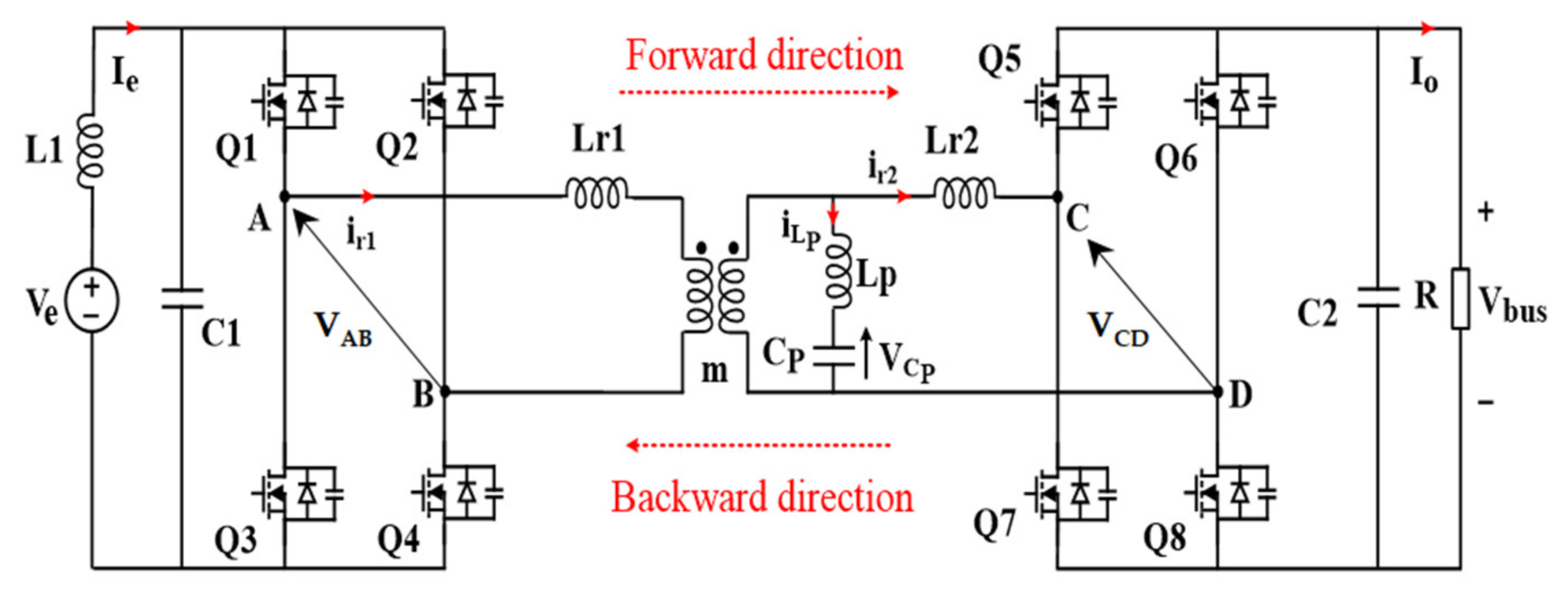
The topology of the proposed resonant converter is presented in Figure 1. It is composed of two active full bridges for bidirectional operations, a high frequency transformer and a symmetric resonant circuit. This last one includes two series inductances (Lr1, Lr2) and a parallel inductance-capacitance (Lp, Cp).
2.1. Forward Mode Analysis
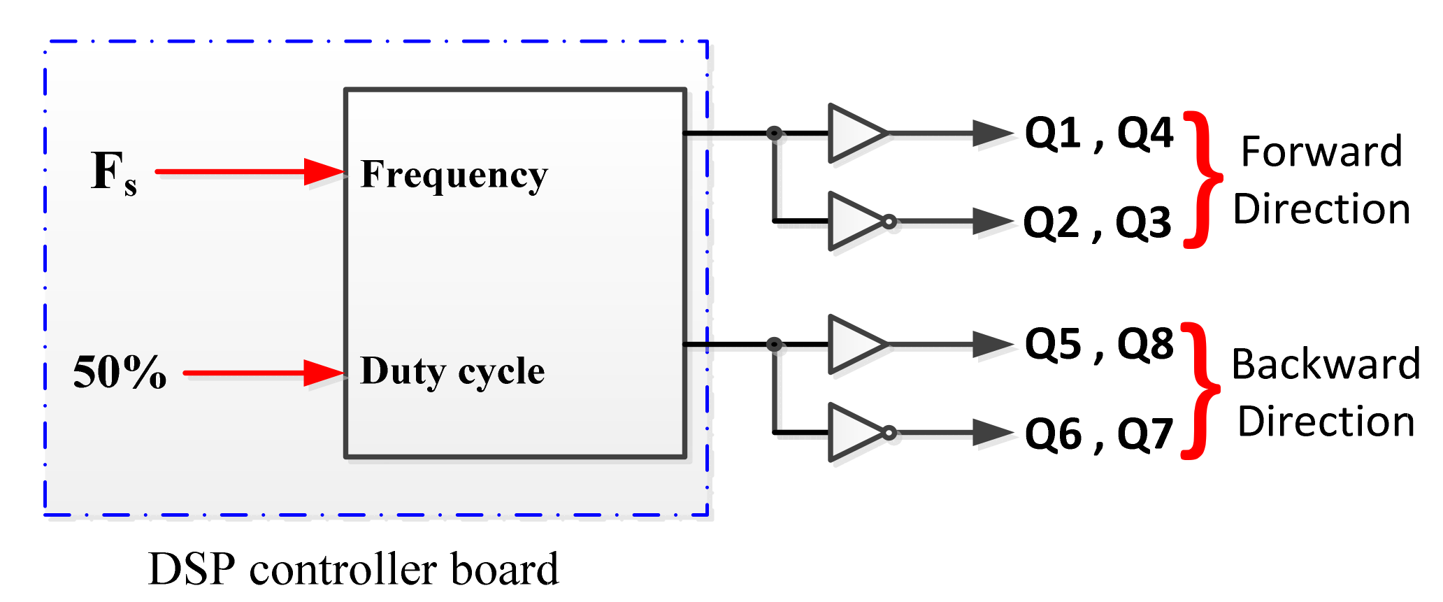
In forward mode, the switches Q1–Q4 are controlled simultaneously using variable frequency PWM signal with a duty cycle of 50%. The switching signals of Q2–Q3 are in complementary logic with Q1–Q4 ones. In this mode, the MOSFET switches of Q5–Q8 and Q6–Q7 at the DC-bus side are turned OFF. So, only the diode rectifier operates in this case. Energy is then forwarded from the DC-source Ve to the DC-bus side Vbus. The voltage between A and B (VAB) of the Figure 1 is a square waveform. It is analytically expressed by Equation (1), where n is the harmonic frequency order, and f1 is the fundamental frequency.
First Harmonic Approximation (FHA) is adopted assuming the active energy is mainly attached to the fundamental frequency. This condition is achieved by filtering the current nearby the resonant frequency of the LC–LL circuit. Fundamental of is given in (2). More information about the method can be found in [18].
The output voltage of the resonant circuit given in Figure 1 is also assumed as a square wave form, and its fundamental component is given in (3), where φv is the phase angle.
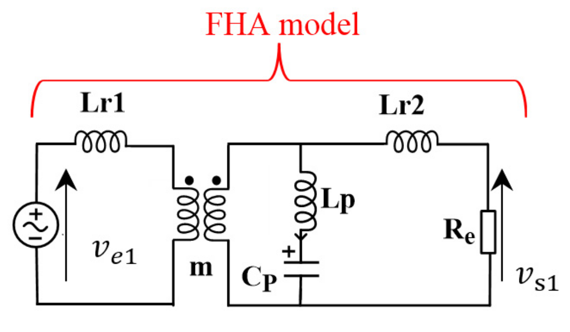
The output impedance through the diodes bridge is reflected by an equivalent resistance Re expressed in (4). R is a resistance-like load on DC-bus [34], and I0 is the average current from the rectifier. The FHA model of the converter is presented in Figure 2 and the corresponding analytical model is given in (5).
The voltage gain (G) based on the equivalent model analysis is given in (6).
The FHA response of the proposed circuit can be better analyzed in a per-unit (p.u.) system with the adopted parameters described below:
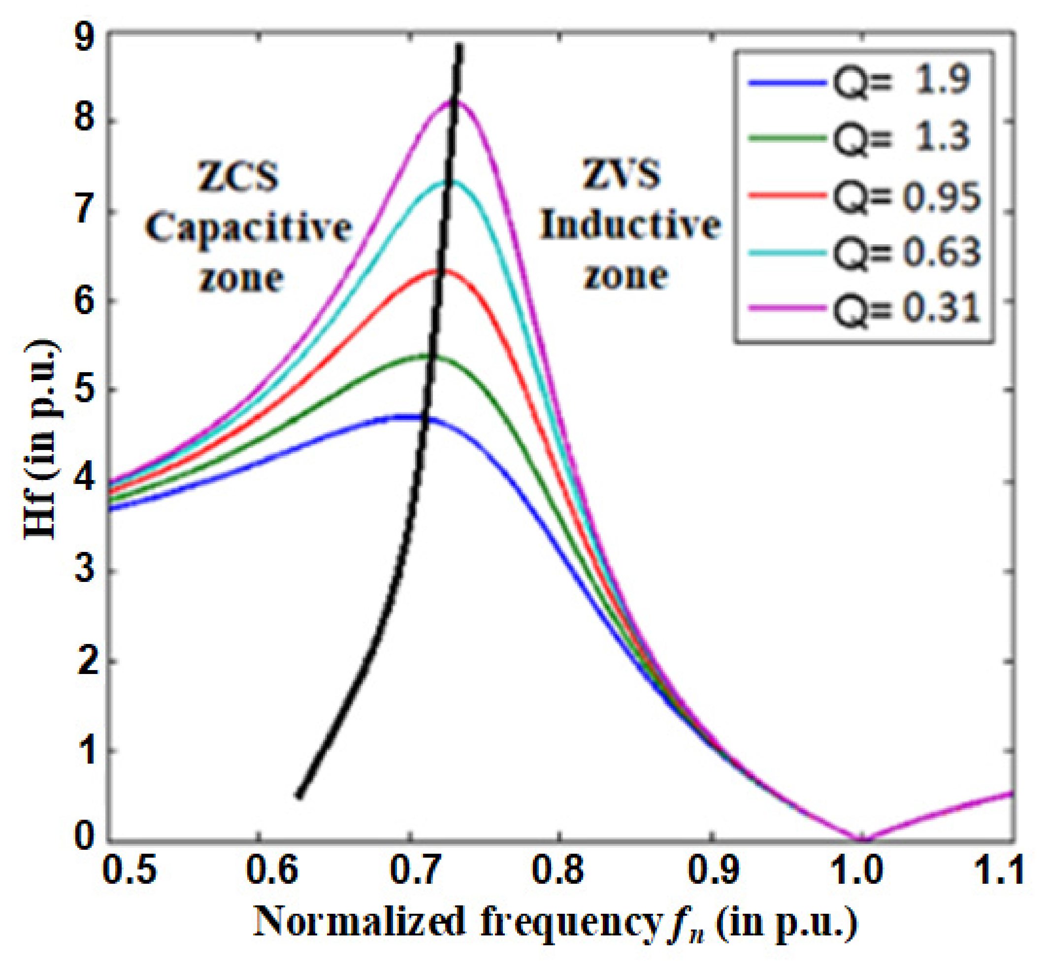
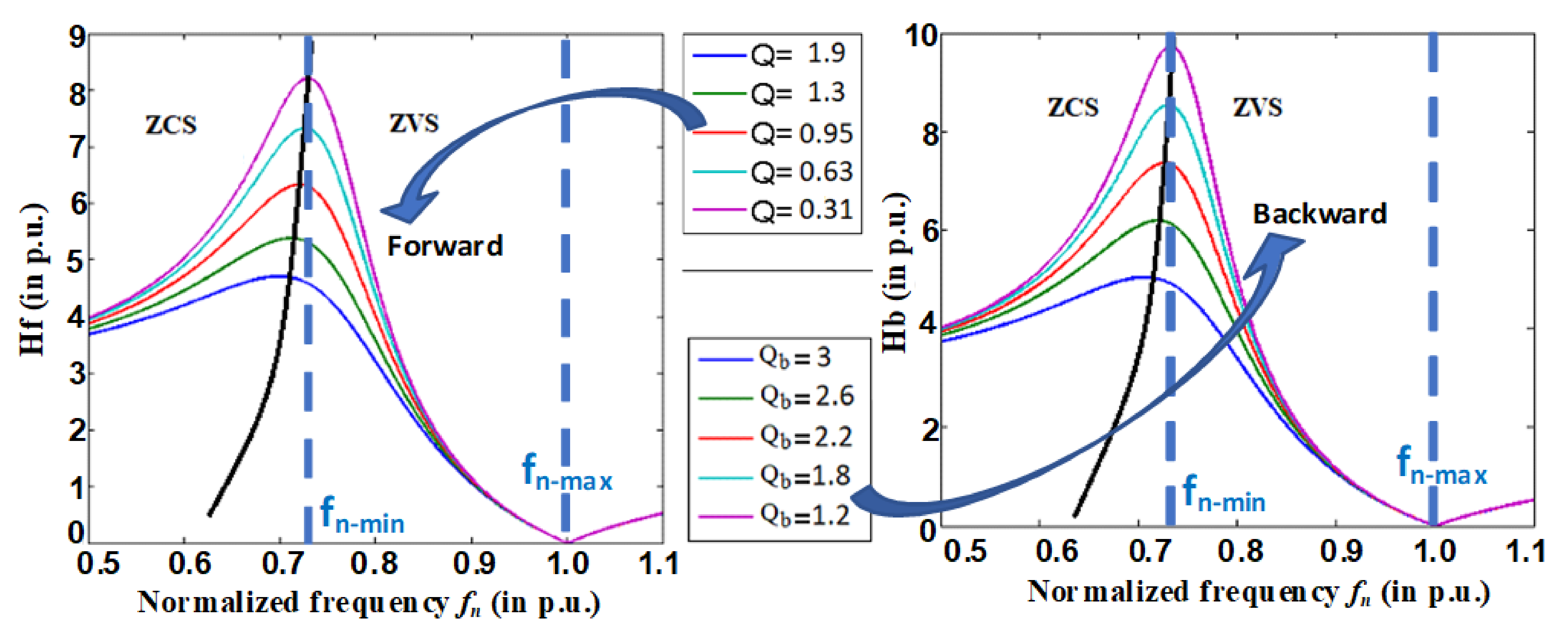
where, is the quality factor, is the normalized frequency, is the series coupled Lp-Cp resonant frequency. and are respectively the normalized values of primary and secondary inductances ratio in per-unit. The resulting output–input DC voltages ratio (Hf) is given in (11).
For , the voltage ratio Hf versus the normalized frequency calculated for different load conditions (i.e., Q) is shown in Figure 3. The favorite operation zone for ZVS is located in 0.72 < fn < 1.
2.2. Backward Mode Analysis
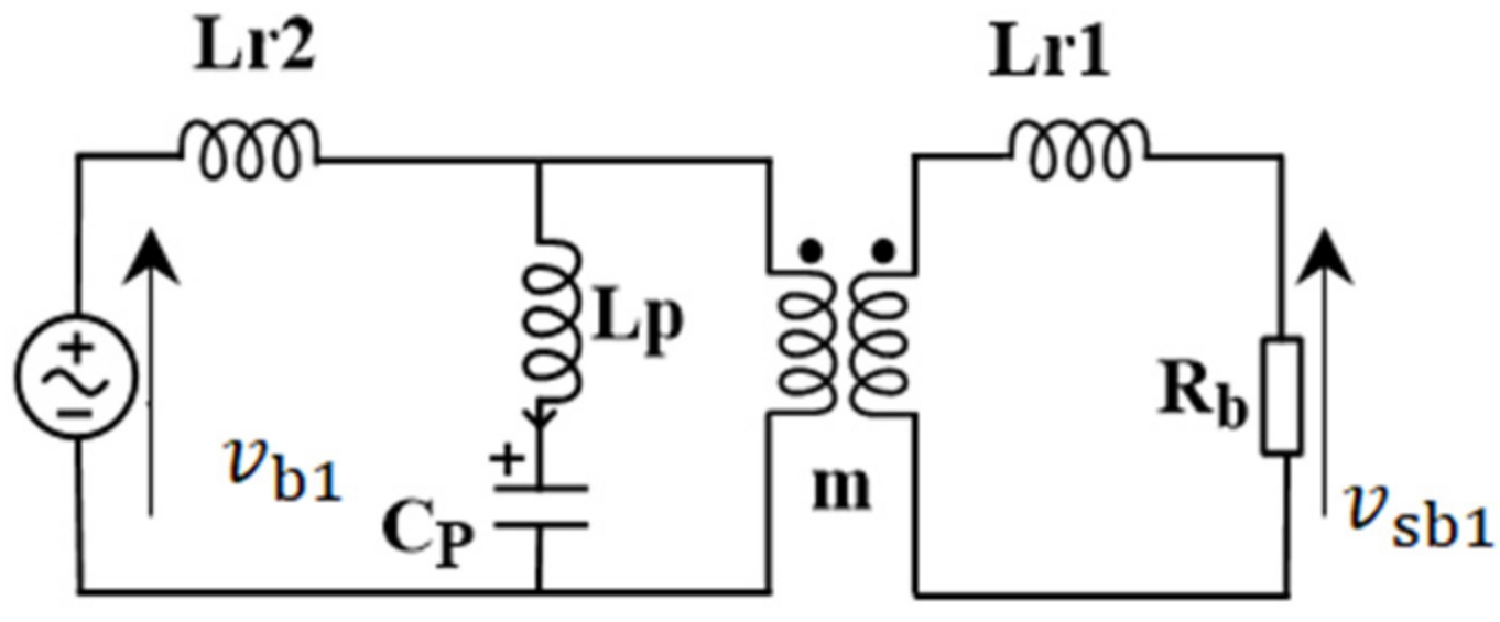
In backward mode of Figure 1, the switches Q5–Q8 and Q6–Q7 are controlled by variable switching frequency. The MOSFET switches of Q1–Q4 and Q2–Q3 are here turned OFF. In this mode, the energy is transferred from the DC-bus to DC-source which is assumed to be reversible (supercapacitors energy storage unit). The equivalent model of the converter in backward mode is presented in Figure 5 and analytical model is given in (12).
The input impedance of the resonant circuit is described in (13). The quality factor is given in (14), and the voltage gain in backward mode (Hb) is presented in (15).
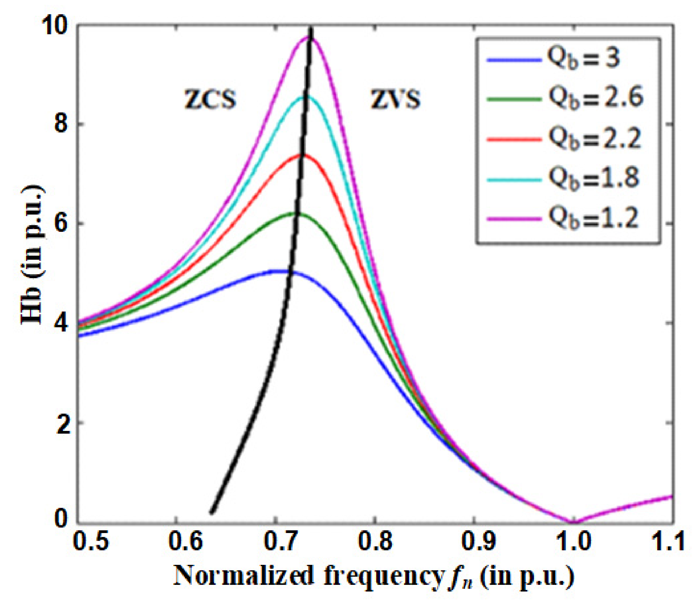
Figure 6 shows the voltage gain of the backward mode versus for different values of the quality factor . We can see that the converter in the backward mode has exactly the same behavior as the forward mode. This means similar operation capabilities in the same restricted frequency domain. If the same tuned values of is assumed, only the quality factor will determine the operation frequency fs within 0.72 < < .
2.3. Operation Principles Analysis
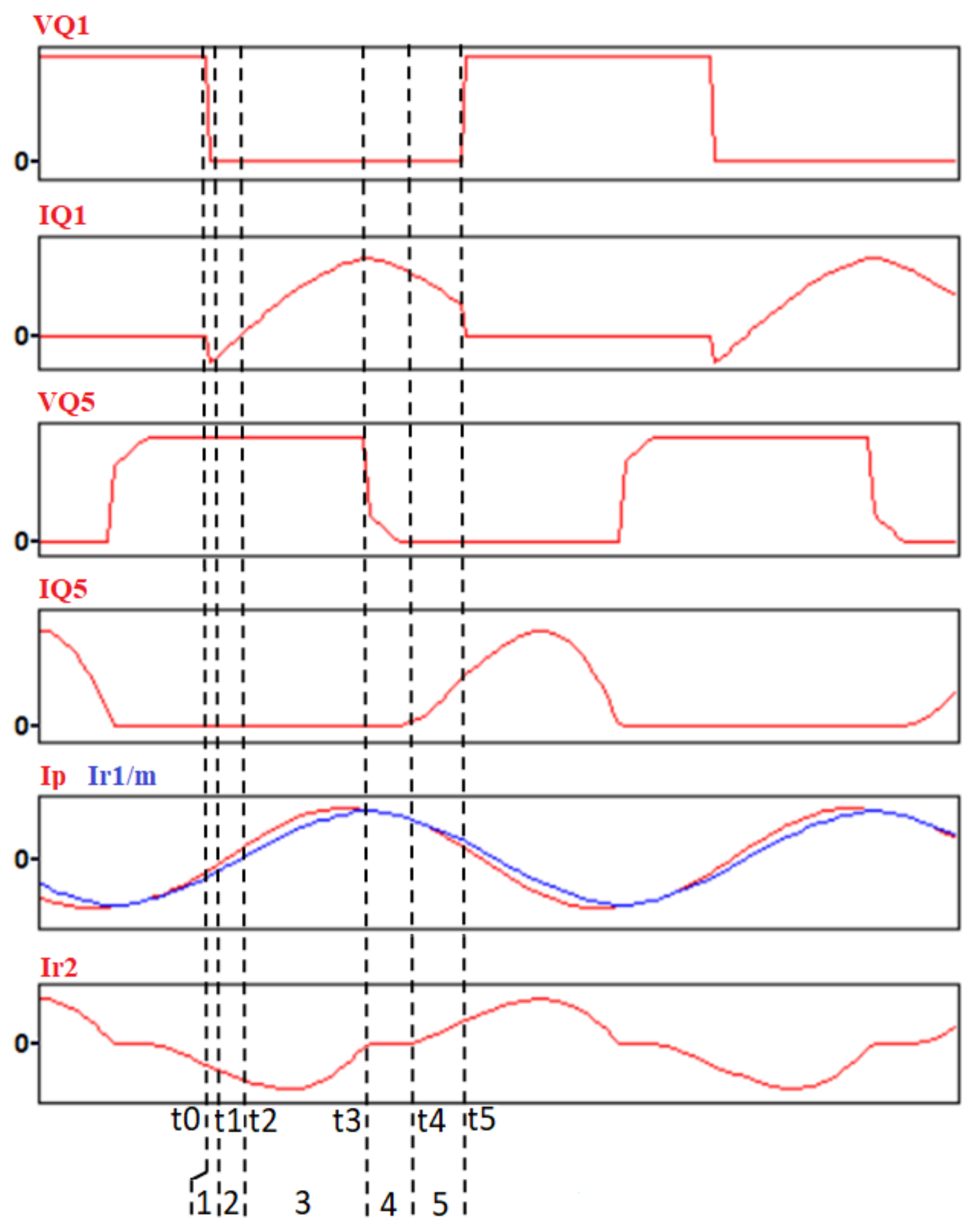
The symmetric bidirectional resonant circuit ensures the same behavior of the converter in both forward and backward modes. Thus, only the principle of the forward operating mode will be discussed in this subsection. Operating waveforms in forward mode are illustrated in Figure 7. Switching conditions are also seen.
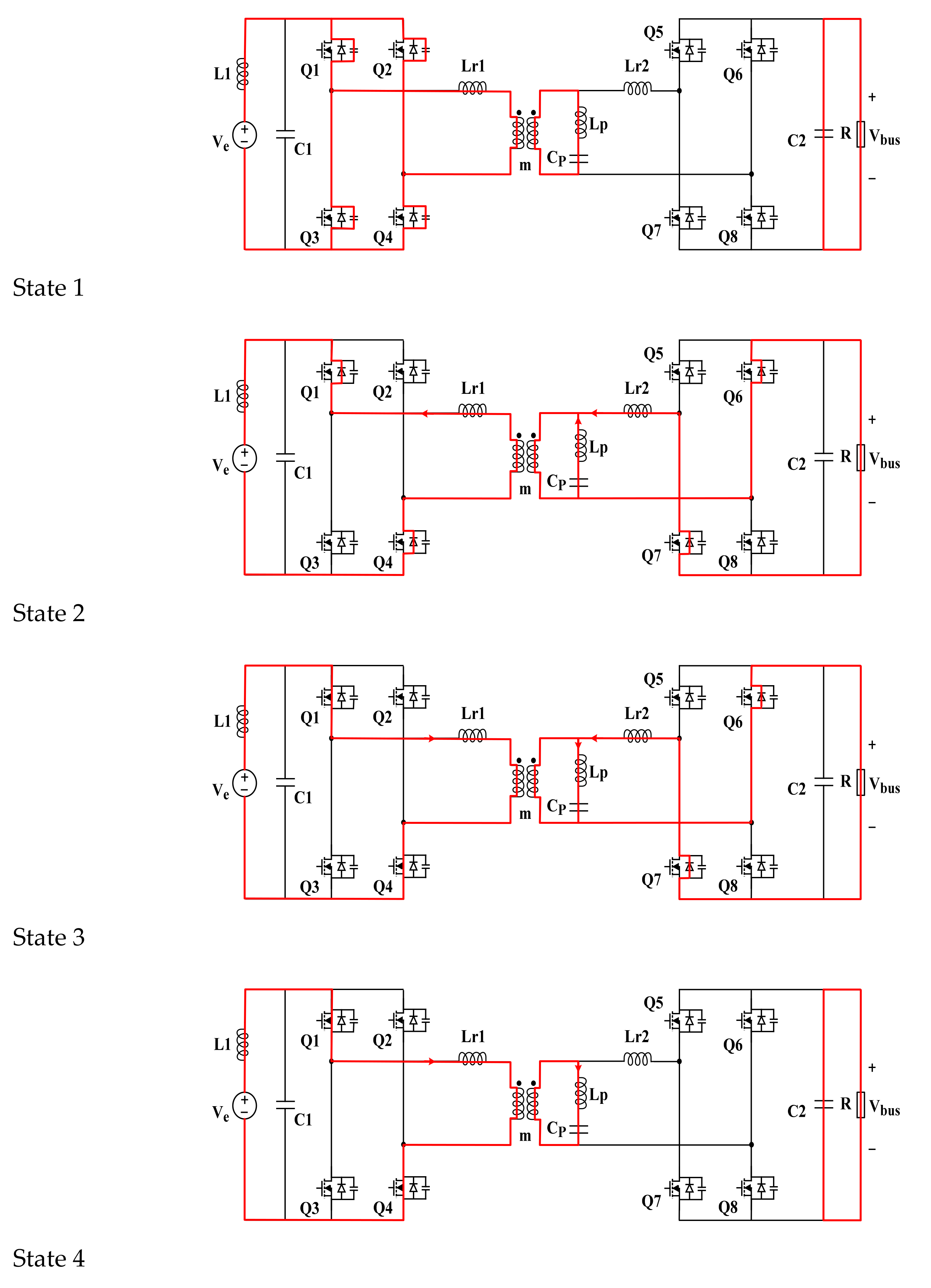
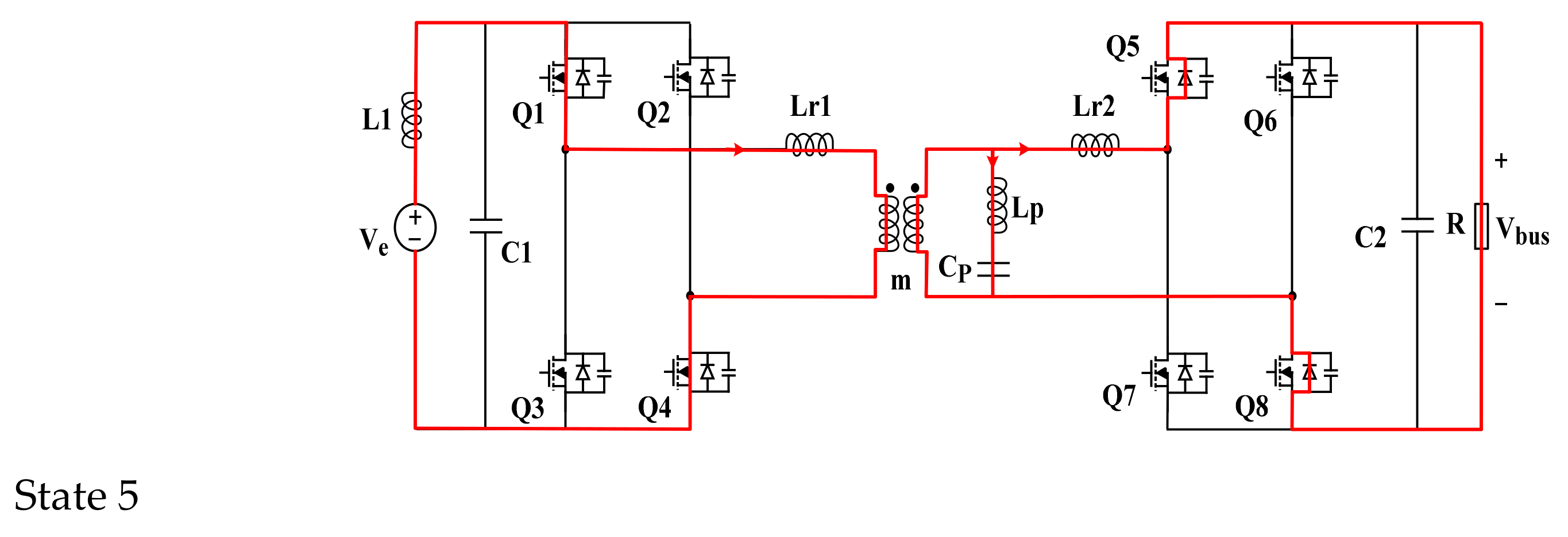
Referring to this figure, the operating states of the converter in forward mode can be divided into five states for a half switching period. The operating sequences are gathered in Figure 8, which shows the active circuits’ paths participating to power exchanges.
State 1 (t0 < t < t1): This mode begins at t0 when Q2 and Q3 are turned off. The current in the inductance Lr1 discharges the parallel capacitor of Q1 and Q4 and charges the parallel capacitor of Q2 and Q3. This state ends when the voltages across Q1 and Q4 (VQ1, VQ4) go to zero and those of Q2 and Q3 (VQ2, VQ3) reach the input voltage.
State 2 (t1 <t < t2): After the full discharge of the parallel capacitors of Q1 and Q4, the negative resonant current ir1 flows through the diodes of Q1 and Q4. The energy stored in the resonant circuit is fed back to the input side, to discharge the capacitor Cp. The expressions of the currents and voltages of resonant components in this mode are defined as follows:
where,
State 3 ( < t <): At , the resonant current changes the direction and the current flowing trough Q1 and Q4 becomes positive. Thus, Q1 and Q4 turn on with ZVS. The current is negative. Hence, the diodes of Q6 and Q7 are conducting to transfer the energy from the DC-source to DC-bus side. The expressions of different resonant currents and voltages in this mode are given as follows:
State 4 ( < t <): This state begins when the resonant current reaches the magnetizing current. The secondary current becomes zero and the capacitor supplies energy to the load. In the primary side, the resonant current charges the resonant circuit. The expressions of the resonant currents and voltages are given in (24) and (25), respectively.
where,
State 5 ( < t < ): At , the current changes the sign and it becomes positive. Thus, the diodes of Q6 and Q7 turn off with ZCS and the body diodes of Q5 and Q8 turn on to deliver the energy to the load. The resonant currents and voltage in this mode are given by the following equations:
The operating principles analysis for the next half cycle is the same as detailed above.
3. Converter Design Method
The design of the converter must ensure essential criteria to have a better efficiency of the converter in both forward and backward mode. The criteria to be met are as follows:
- The switching frequency must be high to minimize the size of the magnetic and capacity components.
- ZVS for the input switches (inverter) and ZCS-ZVS for the output rectifier diodes should be ensured to reduce the switching losses. The converter must perform that regardless of the direction of energy transfer and terminal voltages conditions within a predefined range.
- The converter should ensure a sufficient voltage gain for all load and input voltage conditions.
- The switching frequency range should be as narrow as possible regardless of the direction of energy transfer, the load and the input voltage conditions. In these conditions, the circulating energy is to be kept reduced.
To ensure these criteria, a design procedure will be presented for a 3 kW resonant circuit test bench. The proposed converter was designed to serve as energy path between a variable DC-source with a voltage range of 60~240 V and a 270 V DC-bus. The maximum power of the converter corresponds to the resistance R and the maximum quality factor is Qmax.
R = 24.3 Ω; Qmax = 1.9
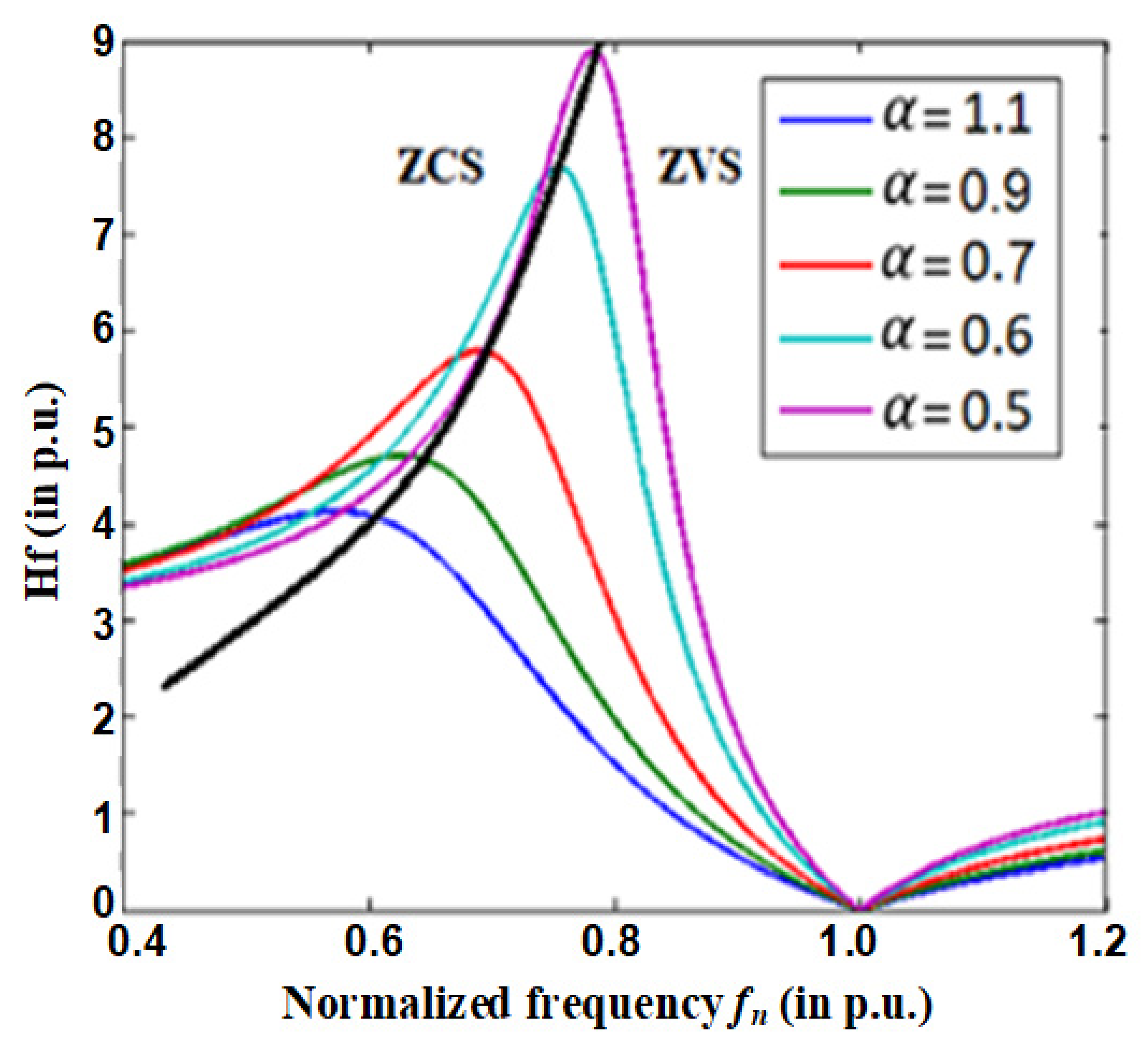
Referring to Figure 4, the maximum voltage gain decreases if increases. The next step is to define the value of that ensures the maximum voltage gain for Qmax. Based on Figure 4, the required maximum voltage gain can be achieved for or less. The switching frequency range and the voltage gain rely on . A small value of involves a narrow switching frequency range. However, should not be very small in order to not induce relatively large size of the inductance . The converter must operate in the ZVS region to ensure soft switching by switches control. The minimum switching frequency is the frequency that gives the maximum voltage gain corresponding to the maximum delivered power. This frequency should be located in the ZVS region, as mentioned previously. The switching frequency increases from the minimum value and the voltage gain decreases until it reaches zero for no-load operation, theoretically corresponding to the resonant frequency . The DC-bus voltage level is controlled to 270 V while the DC-source voltage varies between 60 V and 240 V. So, the converter is with a voltage gain range of 1.1254.5 in forward mode. In backward mode, the converter is in buck mode depending on the changes of roles through transformer terminals and parameters of consequent quality factor Qb.
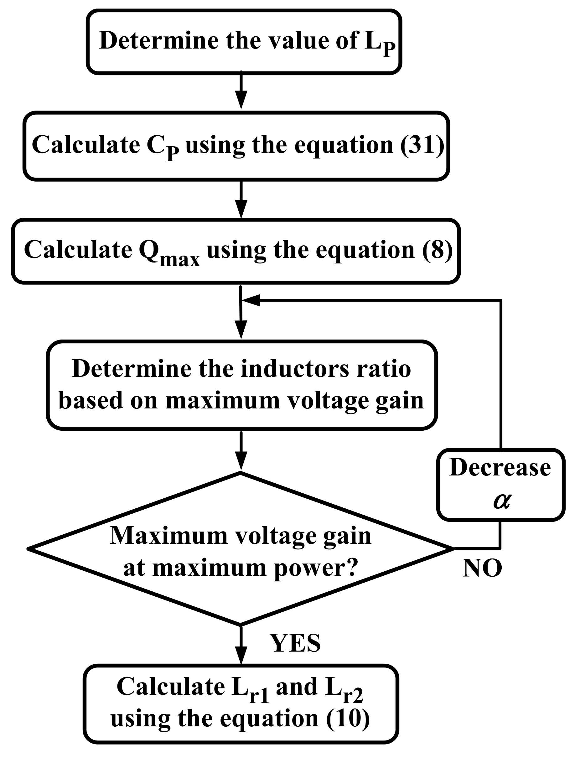
Figure 9 shows the operating regions of the converter in forward and backward modes. The parallel inductance should be chosen to ensure the required voltage gain. A small value of allows to have a high voltage gain with ZVS for all load conditions. However, a very small value of will increase the circulating energy and the conduction losses. Once is defined, is calculated using Equation (10). The critical parameter to respect is the capacitor current to reduce the volume of connected capacitors. For this reason, the parallel components Cp and Lp are placed on the secondary of the transformer with a high transformer turn ratio to decrease the current of the capacitor and to increase the voltage capability. Parallel capacitor is calculated using Equation (31), and the transformer turn ratio is set according to Equation (32). The series inductance is then calculated using Equation (10).
The design procedure of the proposed converter is described in Figure 10.
4. Experimental Test Bench and Results
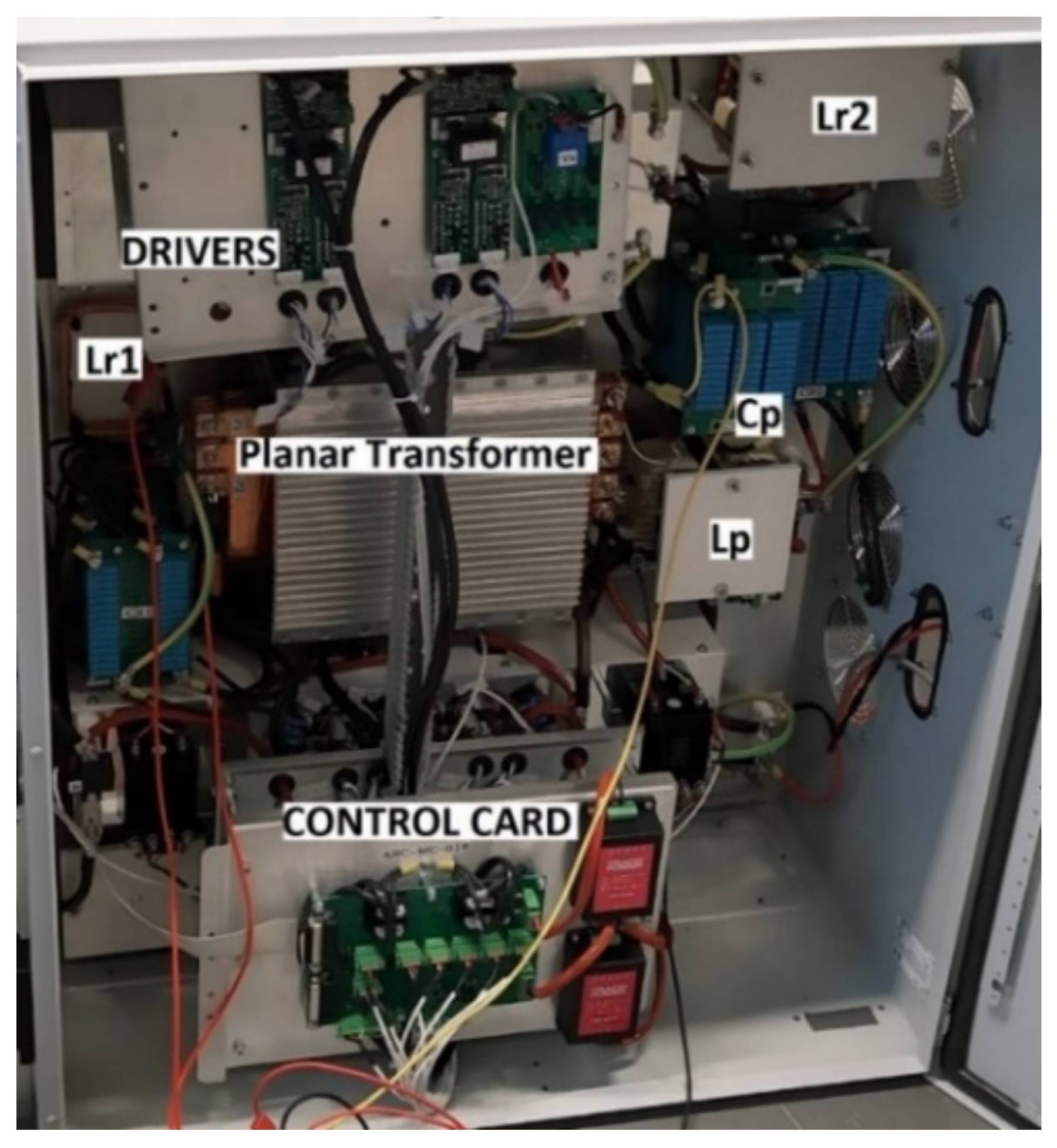
In order to verify the design method and to test the proposed bidirectional resonant converter topology, a laboratory test bench with a 3 kW resonant circuit was built. It was integrated in a 12 kW Dual Active Bridge converter designed for the other laboratory works. The experimental test bench is shown in Figure 11. The characteristics of this test bench are given in Table 2 and the reference of the 800V/39A MOSFETs is IXFN44N80P.
Figure 12 presents the open loop control strategy, where the frequency fs is an input parameter. This switching frequency is adjusted through DS1103 controller board which generates the control signals to maintain the DC-bus voltage at a desired level. To verify the soft-switching over the full operating range of the converter, some experimental tests are done with various input voltage and for different loads powers in both forward and backward mode.
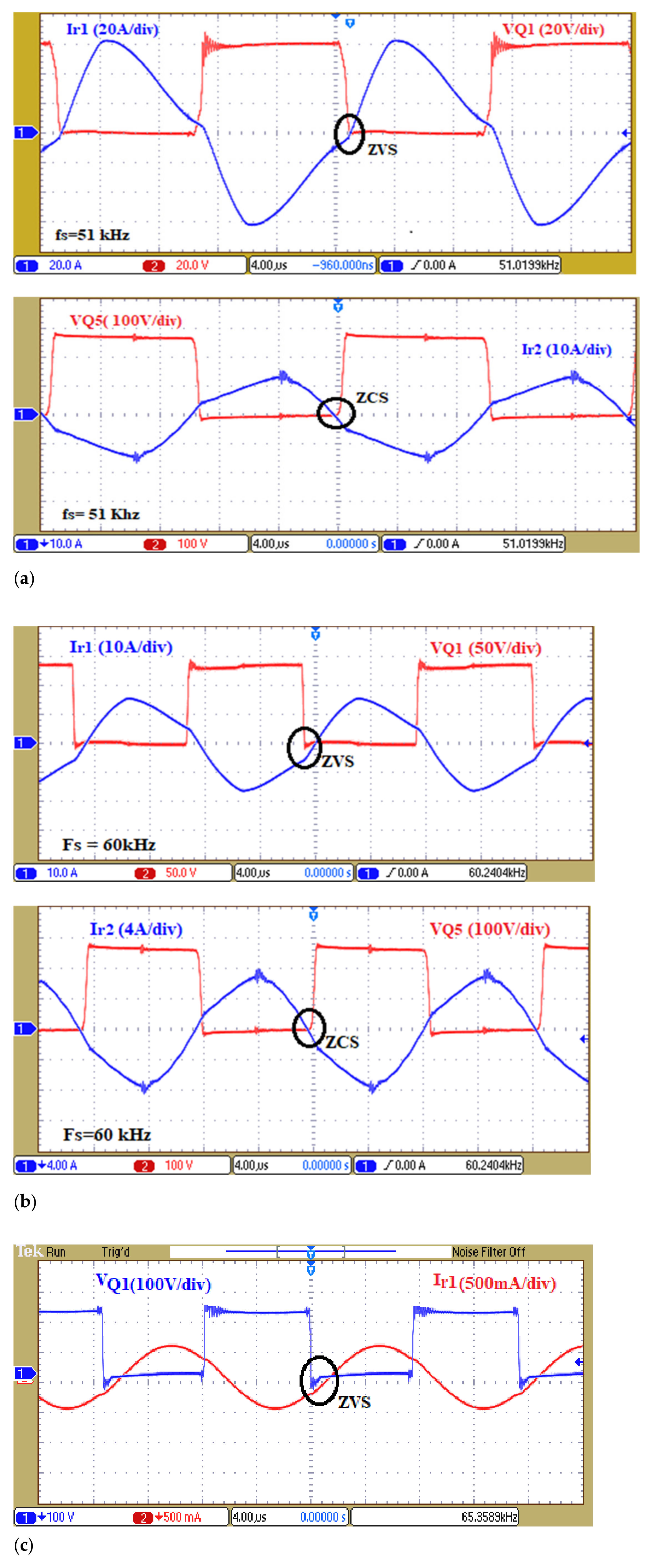
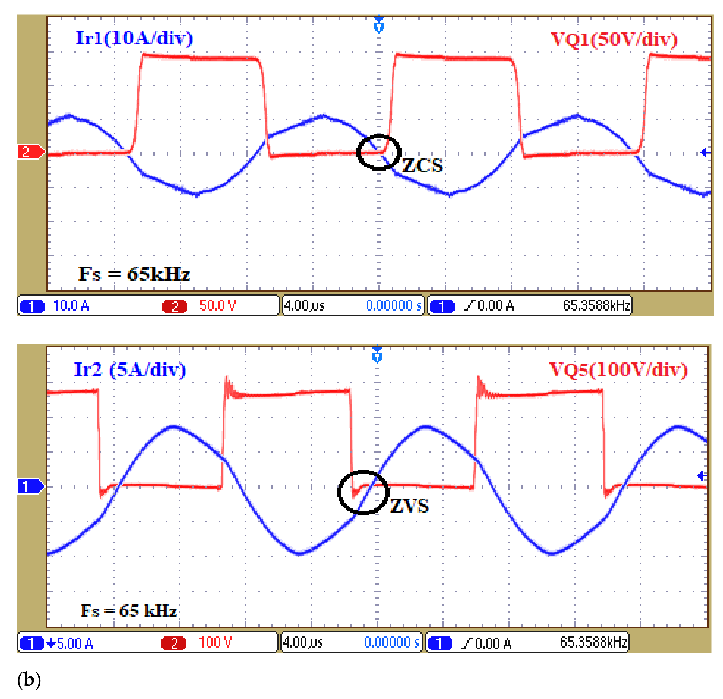
Figure 13 shows experimental waveforms in forward mode. It is seen that ZVS is reached for the primary switches of the inverter. Further, the rectifier diodes turn off with ZCS regardless the load variations and the input voltage value. We also notice the narrow variation of the switching frequency which is typically shown in Figure 3 and Figure 4 with the variations of the load and the input voltage such as:
- fs = 51kHz for Ve = 60 V and P = 3 kW (full load);
- fs = 60 kHz for Ve = 140 V and P = 1.5 kW (half load);
- fs = 60 kHz for Ve = 100 V and P = 0.35 kW (low load).
- fs = 63 kHz for Ve = 240 V and P = 0 kW (no-load).
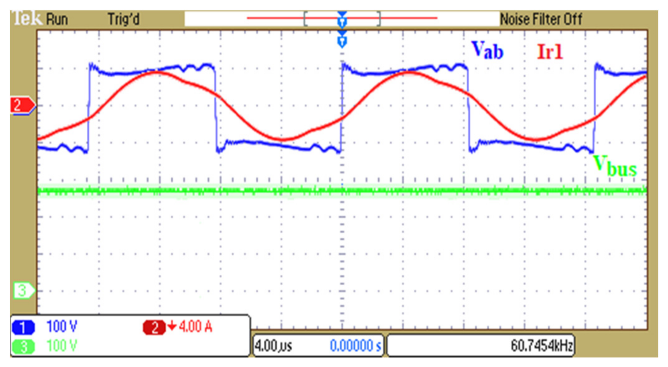
The narrow frequency range reduces internal energy circulating and the turn off losses. Figure 14 presents the Vab voltage at the primary side in forward mode, and the resonant current ir1. We can see that the current lags the voltage. Then, ZVS is always reached.
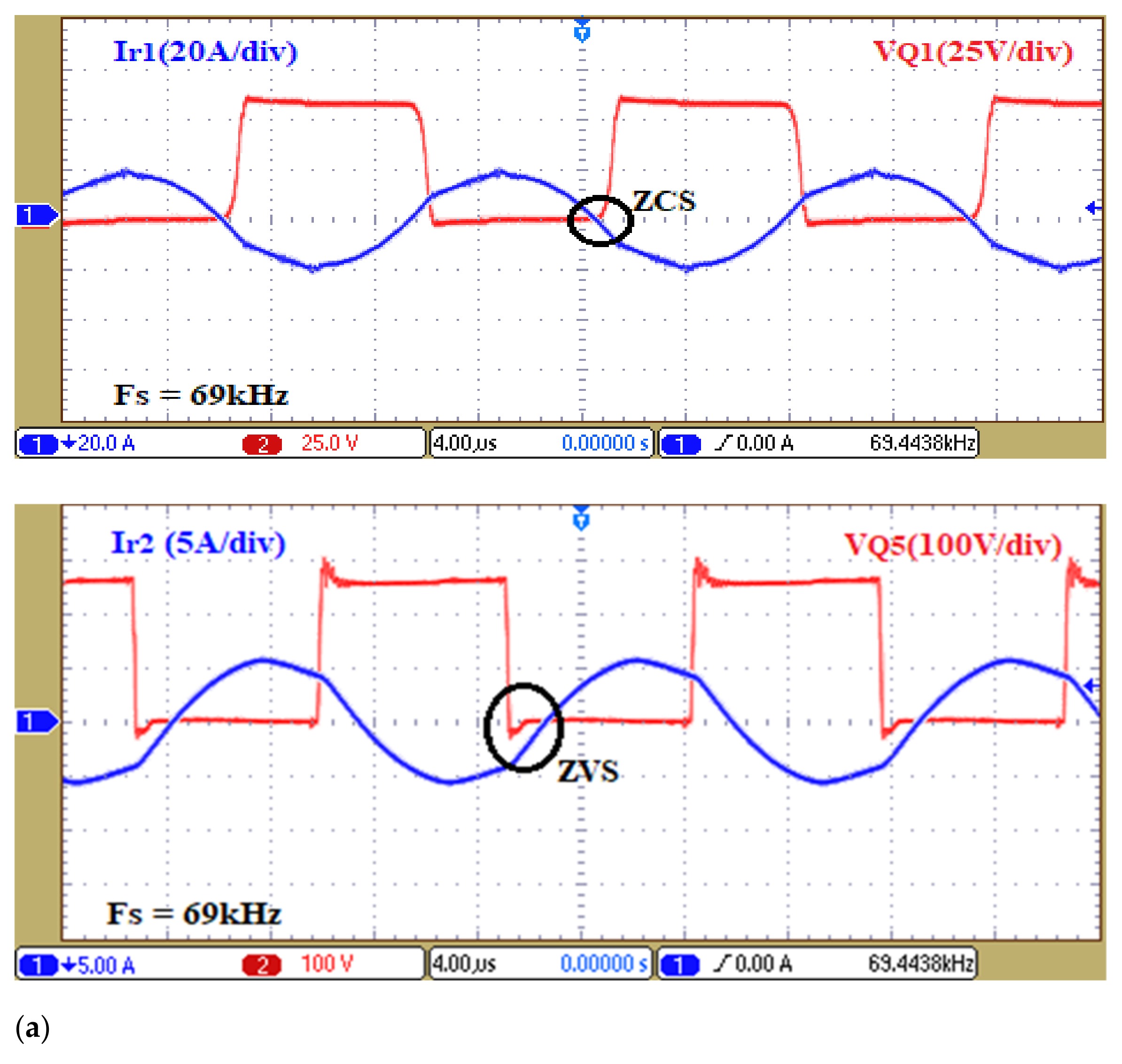
Figure 15 shows experimental waveforms in backward mode for different load conditions and DC-source voltage. The active switches Q5~Q8 are turned on with ZVS and the diodes of Q1~Q4 are turned off with ZCS regardless load and voltage conditions. Note that the switching frequency range in backward mode is also very narrow, which proves also the analyzed behavior in Figure 6.
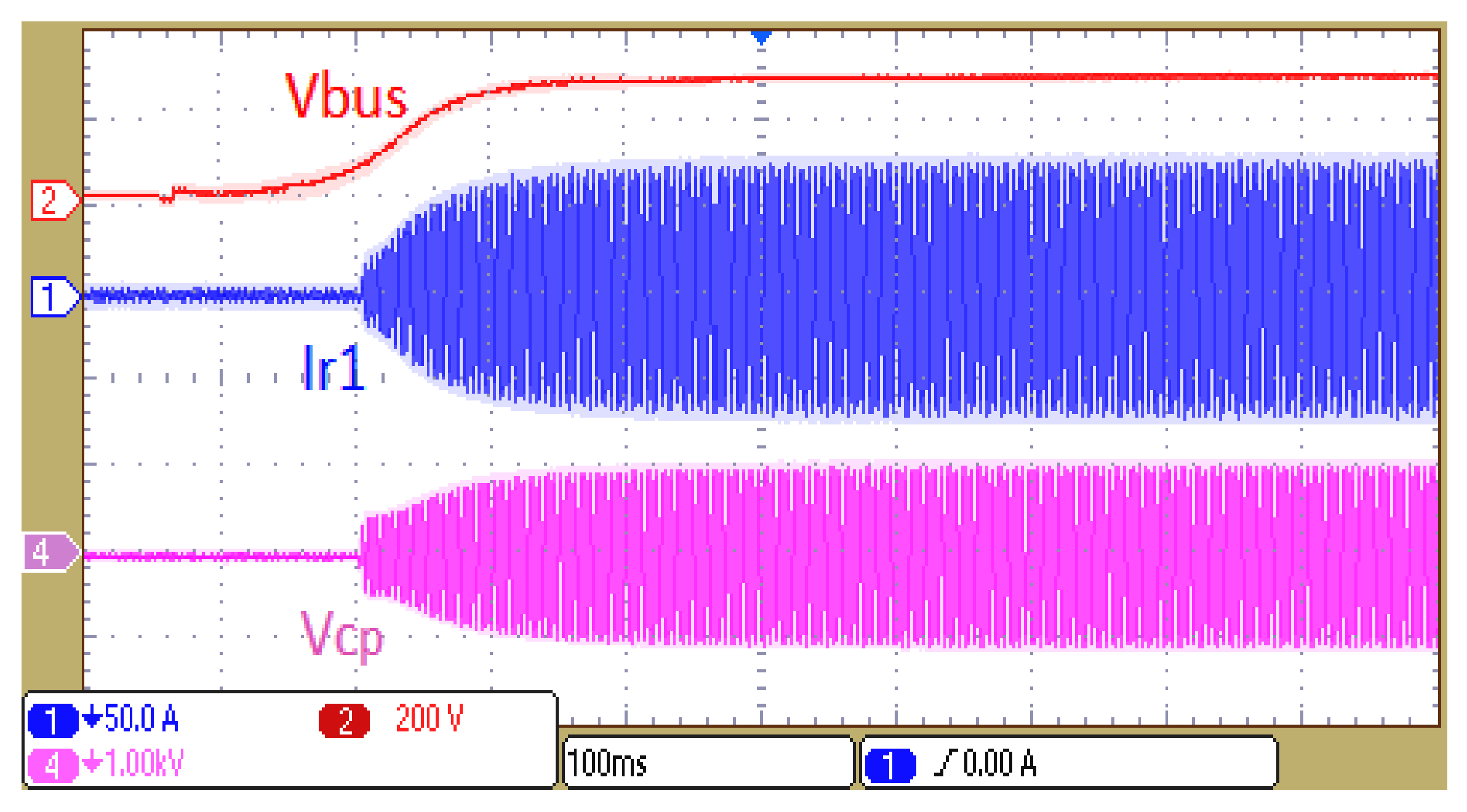
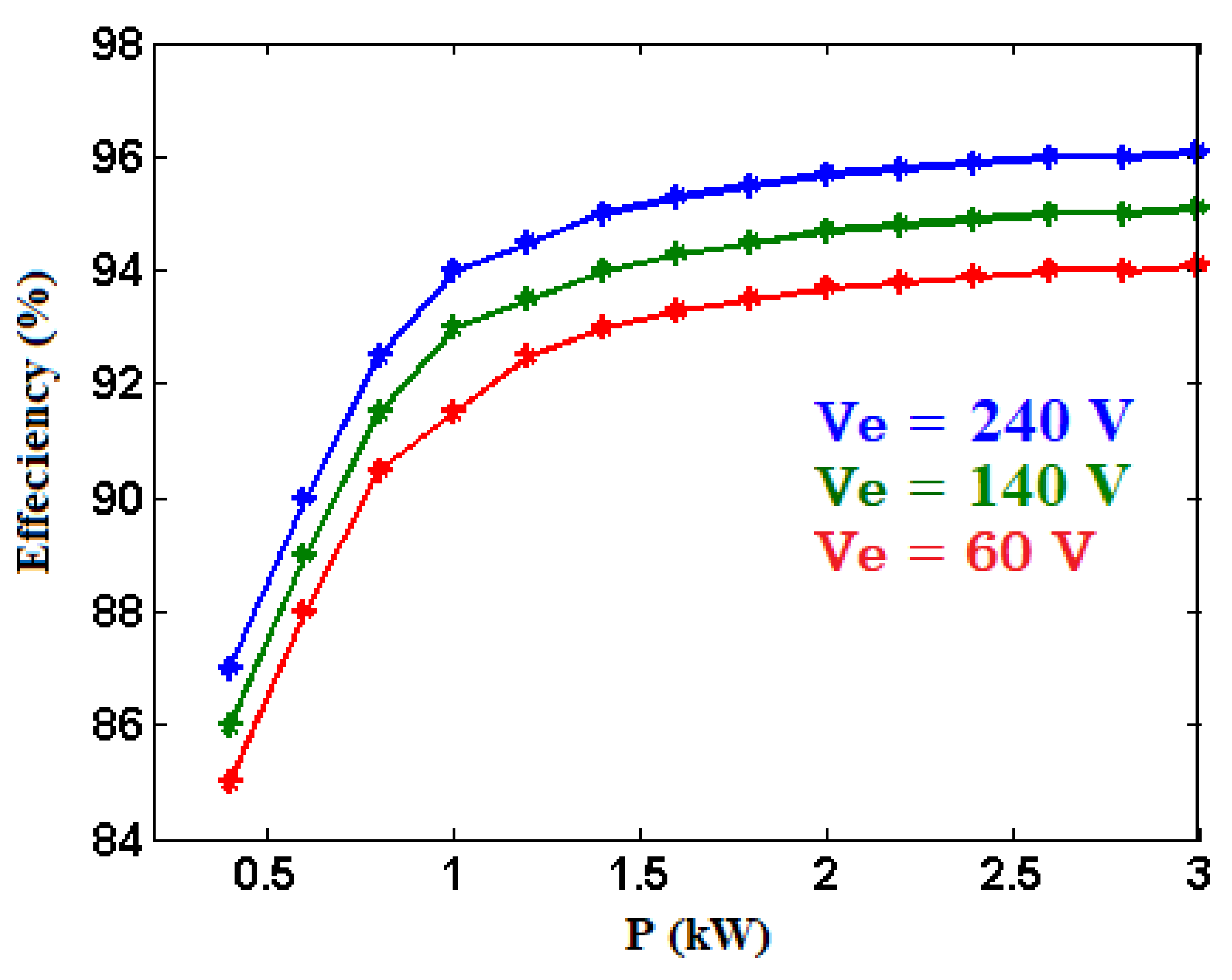
Figure 16 shows the experimental waveforms of , and during startup. We notice the soft startup of the converter with no voltage or current peaks. This is due to the zero-voltage gain at the starting resonant frequency which demonstrates another advantage of the proposed topology. Figure 17 shows the measured efficiency of the converter in forward mode versus the power for different input voltages. The maximum efficiency is about 96% at 3 kW when the DC-source voltage is more significant (240 V in this case). The converter efficiency reduces when the input voltage decreases because the input current increases.
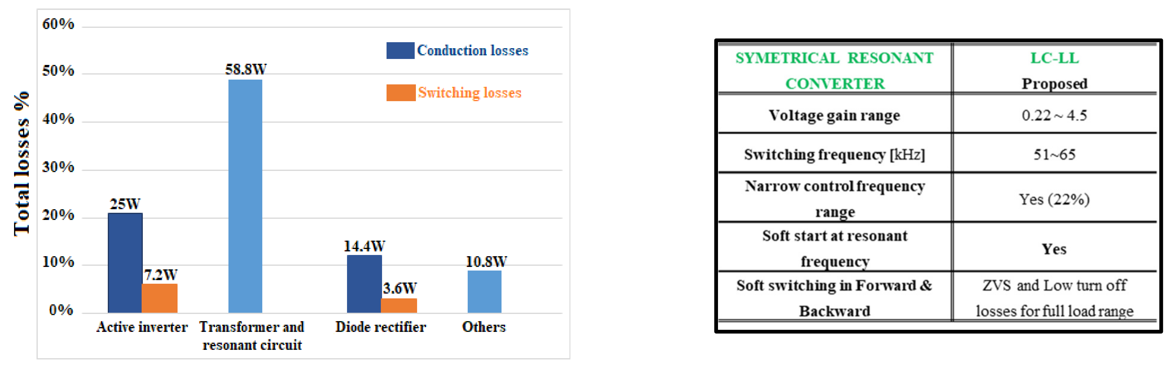
Note that the efficiency of the converter can be increased by using low power loss components with the electric wiring optimizing. Figure 18 presents the power losses distribution in the converter for a full load condition, where the losses in the transformer and the resonant circuit reach 49% of the total losses (120 W). On the other hand, the losses in the active inverter are about 27% of the total losses, while the losses in the diode rectifier are almost 15% of the total losses. The conduction losses are higher compared to those of switching, in order of 3.5 times for the inverter and 4 times for the rectifier. The conduction losses in the inverter reach 21% of the total losses and they are 12% of the total losses in the diode rectifier. Due to soft switching, the switching losses in the inverter and in the rectifier diodes are reduced. They are 6% and 3% of the total losses, respectively. Figure 18 gives also the characteristics of the converter compared to the other ones summarized previously in Table 1.
5. Conclusions
This paper presents a bidirectional resonant converter for wide voltage range applications. Due to the symmetric resonant circuit, the converter has the same behavior in both energies transfer modes. The voltage gain varies from zero to a maximum value in the suitable ZVS region. So, ZVS for active switches of the inverter side and ZCS for the diodes of the rectifier side are achieved regardless the input voltage, the energy transfer direction and the load conditions. Proposed converter topology has the capability to operate under wide voltage range 60~240 V. Control of the power flow is carried out in a predetermined narrow fundamental switching frequency band which increases significantly the efficiency by reducing the circulating energy and the turn off losses. In addition, the proposed converter has no voltage gain at the resonant frequency and so, no specific startup strategy is needed. The experimental results of the 3 kW resonant circuit test bench validate the feasibility of the proposed converter. Moreover, they prove the effectiveness of the proposed design procedure for the developed converter.
Author Contributions
Conceptualization, methodology, validation, formal analysis, investigation, data curation, writing—original draft preparation, writing—review and editing, visualization, M.A., A.P., M.B.C., B.D.; supervision, project administration, funding acquisition, A.P., M.B.C., B.D. All authors have read and agreed to the published version of the manuscript.
Funding
This article has been funded by the council of Normandy Region (France).
Institutional Review Board Statement
Not applicable.
Informed Consent Statement
Not applicable.
Data Availability Statement
The data presented in this study are available on request from the corresponding authors.
Acknowledgments
This work was supported by University of Le Havre Normandy and is funded by Normandy region in France.
Conflicts of Interest
The authors declare no conflict of interest.
References
- Vinnikov, D.; Chub, A.; Kosenko, R.; Zakis, J.; Liivik, E. Comparison of Performance of Phase-Shift and Asymmetrical Pulsewidth Modulation Techniques for the Novel Galvanically Isolated Buck–Boost DC–DC Converter for Photovoltaic Applications. IEEE J. Emerg. Sel. Top. Power Electron. 2016, 5, 624–637. [Google Scholar] [CrossRef]
- Prabhakaran, P.; Agarwal, V. Novel Four-Port DC–DC Converter for Interfacing Solar PV–Fuel Cell Hybrid Sources with Low-Voltage Bipolar DC Microgrids. IEEE J. Emerg. Sel. Top. Power Electron. 2020, 8, 1330–1340. [Google Scholar] [CrossRef]
- Sha, D.; Chen, D.; Zhang, J. A Bidirectional Three-Level DC–DC Converter with Reduced Circulating Loss and Fully ZVS Achievement for Battery Charging/Discharging. IEEE J. Emerg. Sel. Top. Power Electron. 2018, 6, 993–1003. [Google Scholar] [CrossRef]
- Kardan, F.; Alizadeh, R.; Banaei, M.R. A New Three Input DC/DC Converter for Hybrid PV/FC/Battery Applications. IEEE J. Emerg. Sel. Top. Power Electron. 2017, 5, 1771–1778. [Google Scholar] [CrossRef]
- Bellache, K.; Camara, M.B.; Dakyo, B. Transient Power Control for Diesel-Generator Assistance in Electric Boat Applications Using Supercapacitors and Batteries. IEEE J. Emerg. Sel. Top. Power Electron. 2017, 6, 416–428. [Google Scholar] [CrossRef]
- Faraji, R.; Farzanehfard, H. Soft-Switched Nonisolated High Step-Up Three-Port DC–DC Converter for Hybrid Energy Systems. IEEE Trans. Power Electron. 2018, 33, 10101–10111. [Google Scholar] [CrossRef]
- Pires, V.F.; Foito, D.; Cordeiro, A. A DC–DC Converter with Quadratic Gain and Bidirectional Capability for Batteries/Supercapacitors. IEEE Trans. Ind. Appl. 2018, 54, 274–285. [Google Scholar] [CrossRef]
- Wang, L.; Zhu, Q.; Yu, W.; Huang, A.Q. A Medium-Voltage Medium-Frequency Isolated DC–DC Converter Based on 15-kV SiC MOSFETs. IEEE J. Emerg. Sel. Top. Power Electron. 2017, 5, 100–109. [Google Scholar] [CrossRef]
- Sayed, K. Zero-voltage soft-switching DC–DC converter-based charger for LV battery in hybrid electric vehicles. IET Power Electron. 2019, 12, 3389–3396. [Google Scholar] [CrossRef]
- Akagi, H.; Kinouchi, S.-I.; Miyazaki, Y. Bidirectional Isolated Dual-Active-Bridge (DAB) DC-DC Converters Using 1.2-kV 400-A SiC-MOSFET Dual Modules. CPSS Trans. Power Electron. Appl. 2016, 1, 33–40. [Google Scholar] [CrossRef]
- De Din, E.; Siddique, H.A.B.; Cupelli, M.; Monti, A.; De Doncker, R.W. Voltage Control of Parallel-Connected Dual-Active Bridge Converters for Shipboard Applications. IEEE J. Emerg. Sel. Top. Power Electron. 2018, 6, 664–673. [Google Scholar] [CrossRef]
- Xu, G.; Sha, D.; Xu, Y.; Liao, X. Hybrid-Bridge-Based DAB Converter with Voltage Match Control for Wide Voltage Conversion Gain Application. IEEE Trans. Power Electron. 2017, 33, 1378–1388. [Google Scholar] [CrossRef]
- Dung, N.A.; Chiu, H.; Lin, J.; Hsieh, Y.; Liu, Y. Efficiency optimisation of ZVS isolated bidirectional DAB converters. IET Power Electron. 2018, 11, 1499–1506. [Google Scholar] [CrossRef]
- Mukherjee, S.; Kumar, A.; Chakraborty, S. Comparison of DAB and LLC DC–DC Converters in High-Step-Down Fixed-Conversion-Ratio (DCX) Applications. IEEE Trans. Power Electron. 2021, 36, 4383–4398. [Google Scholar] [CrossRef]
- Du, Y.; Bhat, A.K.S. Analysis and Design of a High-Frequency Isolated Dual-Tank LCL Resonant AC–DC Converter. IEEE Trans. Ind. Appl. 2015, 52, 1566–1576. [Google Scholar] [CrossRef]
- Salem, M.; Jusoh, A.; Idris, N.R.N.; Alhamrouni, I. Performance study of series resonant converter using zero voltage switching. In Proceedings of the 2014 IEEE Conference on Energy Conversion (CENCON), Johor Bahru, Malaysia, 13–14 October 2014; pp. 96–100. [Google Scholar] [CrossRef]
- Liu, G.; Jang, Y.; Jovanović, M.M.; Zhang, J.Q. Implementation of a 3.3-kW DC–DC Converter for EV On-Board Charger Employing the Series-Resonant Converter with Reduced-Frequency-Range Control. IEEE Trans. Power Electron. 2016, 32, 4168–4184. [Google Scholar] [CrossRef]
- Outeiro, M.; Buja, G.; Czarkowski, D. Resonant Power Converters: An Overview with Multiple Elements in the Resonant Tank Network. IEEE Ind. Electron. Mag. 2016, 10, 21–45. [Google Scholar] [CrossRef]
- Soeiro, T.; Muhlethaler, J.; Linner, J.; Ranstad, P.; Kolar, J.W. Automated Design of a High-Power High-Frequency LCC Resonant Converter for Electrostatic Precipitators. IEEE Trans. Ind. Electron. 2012, 60, 4805–4819. [Google Scholar] [CrossRef]
- Yang, R.; Ding, H.; Xu, Y.; Yao, L.; Xiang, Y. An Analytical Steady-State Model of LCC type Series–Parallel Resonant Converter with Capacitive Output Filter. IEEE Trans. Power Electron. 2013, 29, 328–338. [Google Scholar] [CrossRef]
- Wei, Y.; Luo, Q.; Mantooth, A. Comprehensive analysis and design of LLC resonant converter with magnetic control. CPSS Trans. Power Electron. Appl. 2019, 4, 265–275. [Google Scholar] [CrossRef]
- Li, M.; Ouyang, Z.; Andersen, M.A.E. High frequency LLC resonant converter with magnetic shunt integrated planar transformer. IEEE Trans. Power Electron. 2018, 34, 2405–2415. [Google Scholar] [CrossRef] [Green Version]
- Kundu, U.; Yenduri, K.; Sensarma, P. Accurate ZVS Analysis for Magnetic Design and Efficiency Improvement of Full-Bridge LLC Resonant Converter. IEEE Trans. Power Electron. 2017, 32, 1703–1706. [Google Scholar] [CrossRef]
- Buccella, C.; Cecati, C.; Latafat, H.; Pepe, P.; Razi, K. Observer-Based Control of LLC DC/DC Resonant Converter Using Extended Describing Functions. IEEE Trans. Power Electron. 2015, 30, 5881–5891. [Google Scholar] [CrossRef]
- Jiang, T.; Chen, X.; Zhang, J.; Wang, Y. Bidirectional LLC resonant converter for energy storage applications. In Proceedings of the 2013 Twenty-Eighth Annual IEEE Applied Power Electronics Conference and Exposition (APEC), Long Beach, CA, USA, 17–21 March 2013. [Google Scholar] [CrossRef]
- Sun, J.; Yuan, L.; Gu, Q.; Duan, R.; Lu, Z.; Zhao, Z. Design-Oriented Comprehensive Time-Domain Model for CLLC Class Isolated Bidirectional DC-DC Converter for Various Operation Modes. IEEE Trans. Power Electron. 2019, 35, 3491–3505. [Google Scholar] [CrossRef]
- Liu, Y.; Du, G.; Wang, X.; Lei, Y. Analysis and Design of High-Efficiency Bidirectional GaN-Based CLLC Resonant Converter. Energies 2019, 12, 3859. [Google Scholar] [CrossRef] [Green Version]
- Zou, S.; Lu, J.; Mallik, A.; Khaligh, A. Bi-Directional CLLC Converter with Synchronous Rectification for Plug-In Electric Vehicles. IEEE Trans. Ind. Appl. 2017, 54, 998–1005. [Google Scholar] [CrossRef]
- Jiang, T.; Zhang, J.; Wu, X.; Sheng, K.; Wang, Y. A Bidirectional Three-Level LLC Resonant Converter with PWAM Control. IEEE Trans. Power Electron. 2016, 31, 2213–2225. [Google Scholar] [CrossRef]
- EKim, E.-S.; Oh, J.-S. High-Efficiency Bidirectional LLC Resonant Converter with Primary Auxiliary Windings. Energies 2019, 12, 4692. [Google Scholar] [CrossRef] [Green Version]
- Zhang, Y.; Zhang, D.; Li, J.; Zhu, H. Bidirectional LCLL Resonant Converter with Wide Output Voltage Range. IEEE Trans. Power Electron. 2020, 35, 11813–11826. [Google Scholar] [CrossRef]
- Jiang, T.; Zhang, J.; Wu, X.; Sheng, K.; Wang, Y. A Bidirectional LLC Resonant Converter with Automatic Forward and Backward Mode Transition. IEEE Trans. Power Electron. 2015, 30, 757–770. [Google Scholar] [CrossRef]
- Zahid, Z.; Dalala, Z.M.; Chen, R.; Chen, B.; Lai, J.S. Design of Bidirectional DC–DC Resonant Converter for Vehicle-to-Grid (V2G) Applications. IEEE Trans. Transporta. Electrif. 2015, 1, 232–244. [Google Scholar] [CrossRef]
- Outeiro, M.T.; Buja, G. Comparison of resonant power converters with two, three, and four energy storage elements. In Proceedings of the IECON 2015—41st Annual Conference of the IEEE Industrial Electronics Society, Yokohama, Japan, 9–12 November 2015. [Google Scholar] [CrossRef]
Figure 1.
Proposed bidirectional topology of novel resonant converter.

Figure 2.
Equivalent model of the proposed converter in forward mode.

Figure 3.
Voltage gain of the converter in forward mode for .

Figure 4.
Voltage gain of the converter in forward mode (Q = 1.9).

Figure 5.
Equivalent model of the converter in backward mode.

Figure 6.
Voltage gain of the proposed converter in backward mode.

Figure 7.
Waveforms of the converter in forward mode.

Figure 8.
Operating states of the converter in forward mode.


Figure 9.
Proposed converter Forward and Backward operating regions.

Figure 10.
Flowchart of the proposed design procedure.

Figure 11.
Proposed resonant converter test bench.

Figure 12.
Open loop control strategy of the converter.

Figure 13.
Experimental waveforms of the converter in forward mode: (a) Ve = 60 V, P = 3 kW (full load); (b) Ve = 140 V, P = 1.5 kW (half load); (c): Ve = 240 V at no load.
Figure 13.
Experimental waveforms of the converter in forward mode: (a) Ve = 60 V, P = 3 kW (full load); (b) Ve = 140 V, P = 1.5 kW (half load); (c): Ve = 240 V at no load.

Figure 14.
Experimental waveforms at P = 0.35 kW and Ve = 100 V.

Figure 15.
Experimental waveforms of the converter in backward mode: (a) Ve = 60 V, P = 1 kW; (b) Ve = 140 V, P = 1.5 kW.
Figure 15.
Experimental waveforms of the converter in backward mode: (a) Ve = 60 V, P = 1 kW; (b) Ve = 140 V, P = 1.5 kW.


Figure 16.
Startup experimental waveforms: where Vbus is the DC-bus voltage, ir1 is the primary resonant current and vCp is the capacitor voltage.
Figure 16.
Startup experimental waveforms: where Vbus is the DC-bus voltage, ir1 is the primary resonant current and vCp is the capacitor voltage.

Figure 17.
Efficiency of the converter in forward mode versus the power for different input voltages.
Figure 17.
Efficiency of the converter in forward mode versus the power for different input voltages.

Figure 18.
Losses distribution and criteria fulfillment of the novel resonant converter.


Table 1.
Comparison of bidirectional resonant converters for wide voltage range applications.
| LCLL [31] | LLC-L [32] | CLLC [33] | |
|---|---|---|---|
| Range of the voltage gain | 0.62~1.125 | 3~5.3 | 0.55~1.12 |
| Switching frequency (kHz) | 65~120 | 60~100 | 40~145 |
| Obtained frequency range percentage | 45% | 40% | 72% |
| Soft start at resonant frequency | No | No | No |
| Soft switching in Forward & Backward | ZVS for full load range; High turn off losses at light load | ZVS for full load range; High turn off losses | ZVS for full load range; High turn off losses |
Table 2.
Characteristics of the built test bench.
| Parameters | Value |
|---|---|
| Input voltage range | 60~240 V |
| Output voltage | 270 V |
| Maximum power | 3 kW |
| Maximum input current | 50 A |
| Switching frequency range | 50~70 kHz |
| Resonant frequency | 70 kHz |
| Transformer turn ratio | 1:4 |
Publisher’s Note: MDPI stays neutral with regard to jurisdictional claims in published maps and institutional affiliations. |
© 2021 by the authors. Licensee MDPI, Basel, Switzerland. This article is an open access article distributed under the terms and conditions of the Creative Commons Attribution (CC BY) license (https://creativecommons.org/licenses/by/4.0/).
Share and Cite
MDPI and ACS Style
Arazi, M.; Payman, A.; Camara, M.B.; Dakyo, B. Bidirectional Interface Resonant Converter for Wide Voltage Range Storage Applications. Sustainability 2022, 14, 377. https://0-doi-org.brum.beds.ac.uk/10.3390/su14010377
AMA Style
Arazi M, Payman A, Camara MB, Dakyo B. Bidirectional Interface Resonant Converter for Wide Voltage Range Storage Applications. Sustainability. 2022; 14(1):377. https://0-doi-org.brum.beds.ac.uk/10.3390/su14010377
Chicago/Turabian StyleArazi, Mouncif, Alireza Payman, Mamadou Baïlo Camara, and Brayima Dakyo. 2022. "Bidirectional Interface Resonant Converter for Wide Voltage Range Storage Applications" Sustainability 14, no. 1: 377. https://0-doi-org.brum.beds.ac.uk/10.3390/su14010377
Note that from the first issue of 2016, this journal uses article numbers instead of page numbers. See further details here.