
Developing a Generalized Multi-Level Inverter with Reduced Number of Power Electronics Components


1
Energy Management Research Center, University of Mohaghegh Ardabili, Ardabil 56199-11367, Iran
2
Department of Electrical Engineering, University of Mohaghegh Ardabili, Ardabil 56199-11367, Iran
3
Faculty of Electrical and Computer Engineering, University of Tabriz, Tabriz 51666-16471, Iran
4
Faculty of Electronics, Communication and Computers, University of Pitesti, 110040 Pitesti, Romania
5
ICSI Energy, National Research and Development Institute for Cryogenic and Isotopic Technologies, 240050 Ramnicu Valcea, Romania
6
Doctoral School, University Politehnica of Bucharest, Splaiul Independentei Street No. 313, 060042 Bucharest, Romania
*
Authors to whom correspondence should be addressed.
Sustainability 2022, 14(9), 5545; https://0-doi-org.brum.beds.ac.uk/10.3390/su14095545
Submission received: 16 March 2022
/
Revised: 10 April 2022
/
Accepted: 27 April 2022
/
Published: 5 May 2022
(This article belongs to the Special Issue Efficiency and Sustainability of the Distributed Renewable Hybrid Power Systems Based on the Energy Internet, Blockchain Technology and Smart Contracts-Volume II)
Abstract
:Reducing the number of components of power electronic converters has been an important research topic over the past few decades. This paper introduces a new structure for a multi-level inverter based on reduced switch basic modules. The proposed basic module requires fewer switches and auxiliary devices. In addition, a lesser number of on-state switches for the synthesis of each voltage level results in less conduction losses, which enhances the converter efficiency. The proposed structure is capable of being implemented in both symmetrical and asymmetrical topologies. This is a merit feature for the proposed topology, which produces high voltage levels with a limited number of elements. The proposed structure is controlled using the fundamental frequency control scheme. The proposed basic module consists of six unidirectional switches and five DC voltage sources, generating five positive voltage levels. The performance of the recommended topology is analyzed from the various circuitry parameters, and a comprehensive comparison carried out with similar recent structures. The presented comparison reveals the advantage of the recommended inverter from different aspects of the circuitry parameters. The suggested structure is simulated using Matlab/Simulink software, and its performance is validated using a laboratory prototype. The results are reported for various steady-state and dynamic conditions.
1. Introduction
Multi-level inverters are widely used in various applications due to their various features, such as low dv/dt stress, modularity, and high-power quality. In high voltage applications, equipment with low and medium voltage levels is often used [1]. Multi-level inverters are usually utilized in high power quality [2], FACTS devices [3], electric vehicles [4], variable speed drives [5], smart grids [6], high voltage applications [7], etc. The traditional multi-level inverters are segmented into three primary categories, which include Diode Clamped Multi-Level Inverter (DC-MLI) or Neutral Point Clamped Multi-Level Inverters (NPC-MLI), Flying Capacitor Multi-Level Inverter (FC-MLI), and Cascade H-Bridge Multi-Level Inverters (CHB-MLI) [8,9]. From the number of circuitry components view, the DC-MLI structure requires multiple diodes if the number of levels increases, making circuit control complex and tedious [1]. In the FC-MLI structure, the voltage balance problem of the capacitors can be solved by using additional switching modes. However, the number of passive components will increase which will be a threat to the reliability of the converter [10]. The CHB-MLI structure is modular and relatively simple compared to the other two topologies. Besides, it does not need additional circuits to match the voltage, but instead uses several isolated DC sources [11]. Despite the simplicity and modularity of CHB-MLIs, adding one module increases four switches and related devices. The need for more circuit devices in the classic topologies of multi-level inverters is a research motivation for new topologies by reducing the number of devices [12].
An advanced configuration was represented in [13] for a symmetrical voltage source multi-level inverter that the high voltage levels are synthesized by extending basic cells. This structure has fewer switches compared to the cascaded H-bridge inverter. However, the number of switches in this topology is still high. In [14], a sub-multi-level structure is introduced, and its cascaded structure was investigated, which requires many switches and drivers. In [14,15], a six-switch H-bridge configuration was utilized for an incremental combination of DC voltage sources. To generalize the voltage levels of this structure, bidirectional switches are considered on both sides of the basic structure. These structures also require a large number of switches. In [16], an extended cascaded structure is introduced, which was based on a basic module and level booster circuit. The number of power electronic devices is high in this structure. An improved symmetric generalized topology was introduced in [17]. This topology consists of two parts, the Level Generation Unit (LGU) and the Polarity Generation Unit (PGU), which uses bidirectional switches. This structure requires a high number of switches, and also the total blocking voltage is significant. In [18], a multi-level cascaded inverter structure was introduced with a new design in symmetrical and asymmetrical topologies, where the number of switches is relatively high. In [19], a bidirectional cascaded multi-level inverter topology was reported, where can operate in symmetrical and asymmetrical modes. This structure was designed by improving the other two structures, which have fewer switches. However, in this inverter, the number of switches and the blocking voltage are also high. In [20], a multi-level inverter for dynamic loads was suggested, which provides two separate structures for symmetrical and asymmetrical topologies. Its symmetrical structure consists of an advanced cascaded H-bridge with many semiconductors. The reference [21] introduces a symmetrical modular multi-level topology with a relatively low number of switches. However, the voltage sources number in this structure is a high value. The reference [22] introduced a switch-ladder structure for a new multi-level converter. This structure was implemented symmetrically and asymmetrically using unidirectional and bidirectional switches. A diode-containing bidirectional structure for a multi-level inverter was reported in [23], which solves the voltage spike problem in such diode-based structures. However, this structure uses a current sensor to realize the current polarity, complicating the control scheme. Also, a generalized diode-containing bidirectional structure for multi-level inverters was represented in [24]. This structure solved the current sensor problem in [23] yet has many switches and considerable blocking voltage. In [25], a modified K-type multi-level inverter structure was reported, utilizing the cascading method to generalize to higher voltage levels. This structure requires eight unidirectional switches to produce seven levels, while the number of switches is not small. A Cross-Switched T-Type (CT-Type) was presented in [26], which used a T-type inverter embedded on either side of the structure to yield more voltage levels. This inverter can operate symmetrically or asymmetrically, while the number of switches was not reduced.
This paper develops a novel configuration for multi-level inverters with symmetrical and asymmetrical topologies. Fewer power electronic devices and fewer switches in the current path of different voltage levels are the main design goals of the recommended topology. These goals make the suggested inverter useful for different applications. The main features of the proposed structure are as follows.
- The proposed basic module has a lesser number of switches, which by generalizing the basic module, the proposed extended structure is realized.
- As the number of switches decreases, the axillary circuit number of devices, including the number of gate drivers, snubber circuits, heat sinks, etc., decreases as well, which reduces the cost and volume of the suggested inverter.
- The voltage stress of the recommended basic module switches is low.
- The maximum number of conducting switches in the current path of each voltage level is low for the proposed structure. Thus, the switches total conduction losses are reduced and the efficiency increased.
The rest of this paper is organized as follows. Section 2 presents the configuration of the suggested MLI converter and its functionality. Section 3 compares the recommended structure with other topologies in terms of circuitry parameters, including switches and gate driver’s number, and total standing voltage (TSV) for different voltage levels. Section 4 presents the mathematical equations and simulations related to losses and efficiency. The analysis of the simulation and laboratory results is reported in Section 5, and finally, the conclusions are presented in Section 6.
2. Suggested Structure
2.1. The Reduced Switch Basic Module
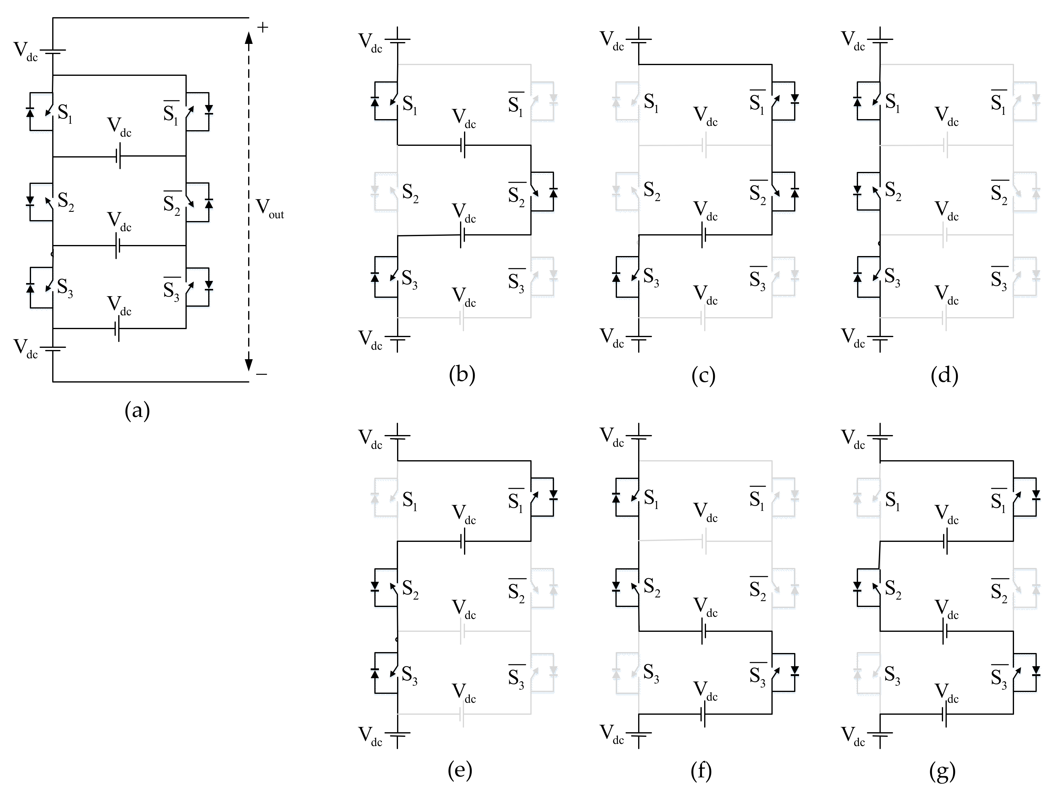
The proposed reduced switch basic module (RSBM) is depicted in Figure 1. It consists of five DC sources and six semiconductor switches along with their anti-parallel diodes. The proposed reduced switch basic module is responsible for producing positive levels. The switches (), (), () of the proposed RSBM operate complementarily. In other words, the conducting switches in the current path of any voltage level are always half of the total switches of the suggested RSBM. The recommended RSBM can produce five positive voltage levels.
The reduced switch basic module consists of three switches S1, S2, S3, and their complementary pairs. According to Figure 1, if the switches S1, S3 are turned on, the output voltage 0 is generated, and if the switch S3 is turned on, the first voltage level is produced. To generate the second voltage level, the switches S1, S2, S3 are turned on, and switches S2, S3 are turned on to generate the third voltage level. The RSBM also generates the fourth voltage level when the switches S1, S2 are turned on, and the fifth voltage level is generated when the switch S2 is turned on. Table 1 demonstrates the switching pattern of the suggested basic module to produce voltage levels. In this table, 1 means on-state, and 0 means off-state for switches. Naturally, complementary switches behave inversely with the main switches.
2.2. Blocking Voltage of the Proposed Reduced Switch Basic Module
Maximum blocking voltage (MBV) indicates the peak voltage across the off-state switch. Considering the MBV of all switches of the converter, the total blocking voltage (TBV) for the converter is obtained, which can be expressed as follows:
The MBV and TBV parameters are an important challenge for multi-level inverters. The parameter MBV is the most important in selecting the voltage rating of switches. The price of the switches is proportional to their allowable voltage rating. Therefore, the lower the MBV value of the converter switches, the lower the total cost. The MBV value for each switch of the proposed basic module is given in the following relations.
The MBV relations of the proposed RSBM reveal that this basic unit can generate five voltage levels using low-voltage rating switches.
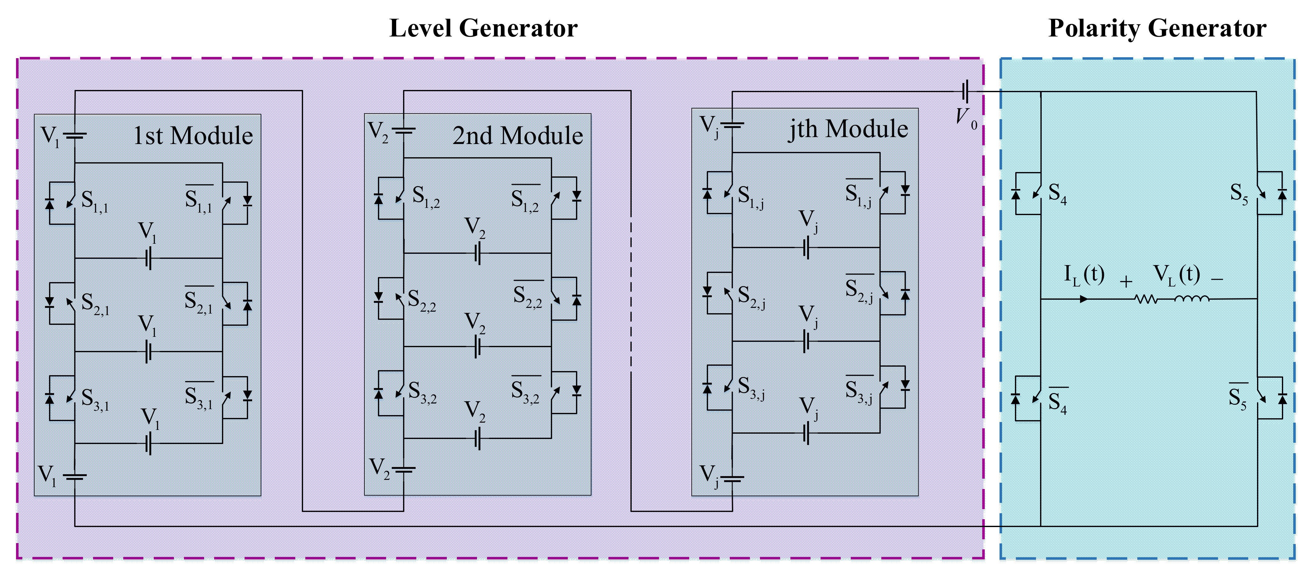
2.3. The Proposed Generalized Inverter Structure
The proposed reduced switch basic module can generate only positive voltage levels. So, a structure must generate positive and negative voltage polarity. The H-bridge module can be used for this purpose. Figure 2 displays the proposed multi-level inverter structure. According to this figure, the proposed structure consists of two parts. The first part is related to the level generator, and the second part is related to the polarity generator. In the proposed multi-level inverter, the reduced switch basic modules are connected in series and form the level generator. All switches of the proposed structure operate complementarily. This means that only half of the switches are in on-state at any output voltage level. In other words, the low number of on-state switches reduces the conduction losses of the switches. The size of voltage sources in the RSBMs can be designed and adjusted both symmetrically and asymmetrically.
In a symmetric topology, the size of voltage sources of the RSBMs is equal. If the voltage source size of the RSBMs is assumed to be Vdc, the following relations provide the various parameters of the proposed multi-level inverter in the symmetric topology.
In the above relations, j shows number of RSBMs, Vj shows the size of the voltage sources of the jth basic module, NL shows the number of output voltage levels that can be synthesized by the topology, NIGBT, and NS show the number of IGBT and switches, respectively. Since the bidirectional switch is not utilized in the structure, the number of switches and IGBTs are equal. NGD shows the number of gate drivers, and the TBV shows the total blocking voltage by the switches of the structure.
In an asymmetric topology, voltage source sizes can have different values using various algorithms. Table 2 presents the allowable algorithms for the size of voltage sources in asymmetric topology, where j represents the jth RSBM.
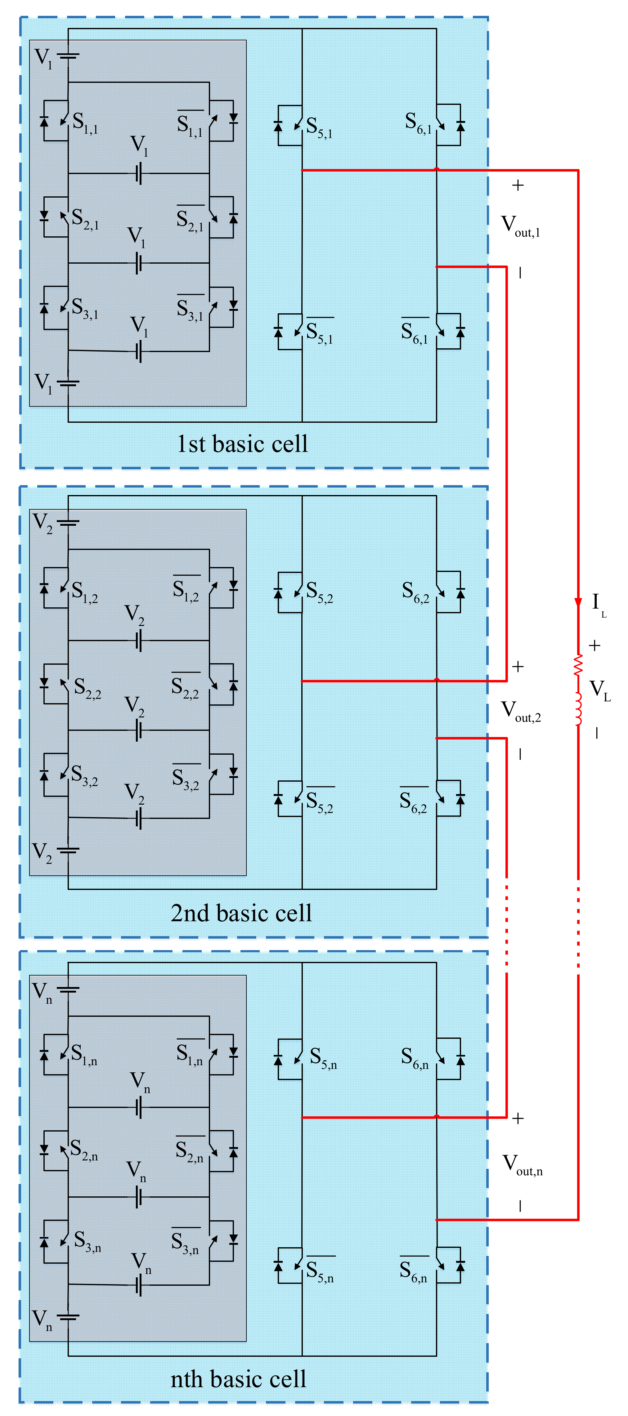
2.4. The Proposed Multi-Level Inverter Structure
The structure shown in Figure 2 with a reduced switch basic module is assumed to be the basic cell. By connecting these cells in series, the cascaded structure of the proposed topology is realized. Figure 3 shows the proposed cascaded topology with n basic cells. The cascading method is also a method for generalizing the proposed structure to achieve high voltage levels by using a small number of sources. In addition, in the cascaded topology, the voltage range of H-bridge switches is limited, and it is possible to achieve medium and even high voltage and power levels using limited Maximum Voltage Blocking (MBV) switches.
In the cascaded topology, the output voltage (VL) is obtained from the output voltage of the multiple basic cells:
In the cascaded topology, different algorithms can be used to generate voltage levels. The cascaded topology can be implemented with the following algorithm.
In this algorithm, the voltage value of independent voltage sources is determined as follows:
In the main structure shown in Figure 2, the voltage sources simply have an incremental combination. However, the voltage sources in the cascaded topology, in addition to incremental combination, can also have a decreasing combination, which leads to a significant increase in the number of output voltage levels. The number of voltage levels, the number of IGBTs, and the number of drivers for the cascaded topology are presented in the following equations.
where n represents the number of basic cells.
One of the advantages of cascaded topology is the replacing capability for the basic cells. If one of the basic cells is damaged, it can be taken out of the circuit, and the structure will continue to work with fewer voltage levels.
3. Efficiency Calculation
In this section, the calculation and simulation of the conduction losses and switching losses are presented to estimate the efficiency of an 11-level basic cell. The conduction losses are divided into two parts: switch conductance losses and anti-parallel diode conduction losses. A detailed analysis of the power losses of a power electronic converter is investigated in the following.
3.1. Conduction Losses
Power electronic switches have conduction losses when conducting the current in ON-state. The conduction losses of the switch and its anti-parallel diode is calculated by the following equations:
where S indicates the switch and D indicates the diode. The voltages vs. and VD are the voltage drop across the switch and the anti-parallel diode in their conduction interval. The resistors RS and RD represent the equivalent resistance of the switch and its anti-parallel diode, i(t) is the current flowing through the switch and the anti-parallel diode at the conduction moments. The parameter α is a switch constant that depends on the switch specifications, which is introduced by the manufacturer in the switch datasheet. The conduction losses are calculated from the sum of the conduction losses presented in Equations (14) and (15). The amount of conduction losses of a multi-level inverter depends on the number of switches conducted at different voltage levels. Considering NS as the conducting number of switches and ND as the conducting anti-parallel diodes in a time interval, the average conduction losses of the converter in an output voltage period can be represented by (16):
3.2. Switching Losses
The switching losses are based on the energy losses due to the non-ideal switch performance. The energy losses include switch ON and OFF losses calculated by Equations (17) and (18):
which EON,j and EOFF,j are the energy dissipation of the switch j at the moments of turning on and off, and are the time intervals required to turn a switch on and off, respectively. The parameters I and are the current that passes through the switch before turning it off, and after turning it on. VS,j is the reverse voltage across the switch after it is turned off. The switching power losses of switches in an output voltage period can be written as follows:
which NON,j and NOEE,j are the number of times that switch turns on and off in a cycle, and f is the output voltage frequency. Finally, the total losses are calculated by Equation (20):
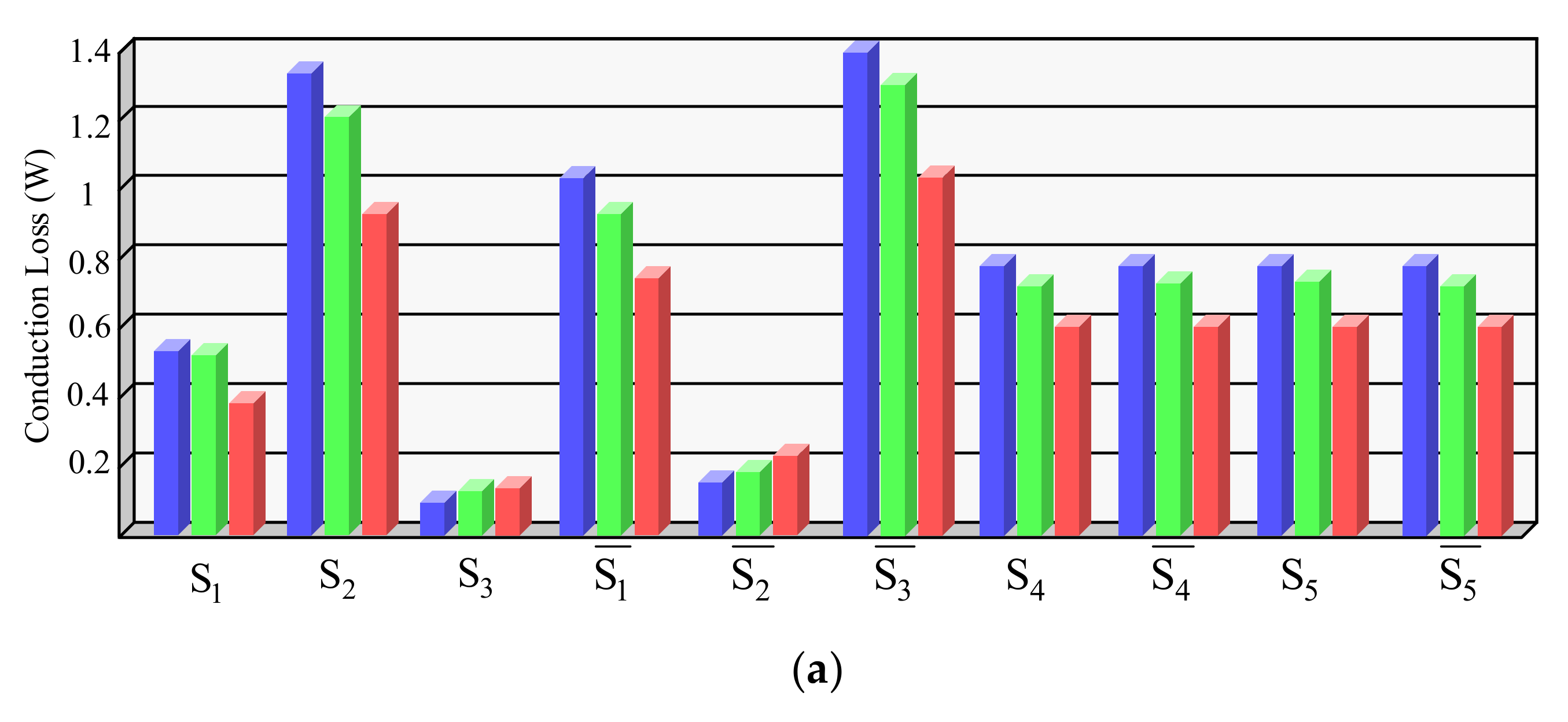
To investigate the efficiency of the proposed 11-level basic cell, power losses on proposed MLI at the output loads Z1 = 50 Ω, Z2 = 50 + j12.56 Ω, and Z3 = 50 + j25.12 Ω are simulated with output voltage steps of 50 V. Figure 4a, b show the conduction and switching power losses for all three types of the loads, respectively. Besides, the efficiency and total losses are also displayed in Figure 4c. To compare the efficiency of the proposed 11-level structure, the efficiency curve for different output power is shown in Figure 5.
4. Comparative Study
In this section, the proposed topology is compared with other recent topologies presented in [13,14,15,16,17,18,19,20,21,22,23,24,25,26,27,28,29,30,31] to evaluate the validity and capability of the proposed MLI. For a fair comparison of the structures, a graph of the number of switches to different voltage levels is presented, and in addition, the NIGBT/NL ratio is calculated and presented in Table 3 for the proposed basic module and the comparative structures. Moreover, Table 3 lists other comparative parameters, including NIGBT (number of IGBTs), NGD (number of drivers), NL (number of voltage levels synthesized by structure), NDC (number of DC voltage source), TBV (total blocking voltage), ND (number of Diodes) and NIGBT, ON (number of conducting IGBTs in each voltage level) for the proposed topology and other symmetric topologies. According to this Table, the presented basic module utilizes fewer switches for various voltage levels.
To fairly compare the number of IGBTs in the proposed structure with other structures, a graph of the number of IGBTs relative to the number of voltage levels (NIGBT/NL) is evaluated. This ratio also provides cost-effectiveness of structures. The larger this ratio, the steeper the slope of the comparison curve, and the more IGBTs are used to achieve higher output voltage levels. Furthermore, the smaller this ratio, the lower the slope of the comparison curve, and the fewer IGBTs are required.
As shown in Figure 6a, using the proposed structure, a large number of voltage levels can be achieved with a smaller number of IGBTs, which produces high-quality output voltage with a smaller number of switches. Some structures use bidirectional common-emitter switches, which makes the number of gate drivers different from the number of IGBTs. For a fair comparison of the number of gate drivers of the proposed structure with other structures, the ratio of the number of gate drivers to the number of voltage levels (NGD/NL) is presented. Figure 6 demonstrates the (NIGBT/NL) and (NGD/NL) diagrams for the proposed and other structures. As shown in Figure 6a, the proposed topology has the lowest slope for (NIGBT/NL) diagram, which means the proposed structure utilizes the lowest number of switches to generate different voltage levels. Figure 6b also shows a comparison of the number of gate drivers, in which the proposed structure does not have the lowest curve slope regarding the number of gate drivers since it has not utilized a bidirectional switch. Nevertheless, the proposed structure still has a relatively good condition regarding the number of gate drivers compared to most comparative structures.
The total blocking voltage (TBV), the sum of the maximum blocking voltage (MBV) of the converter switches, is an essential parameter in comparing and evaluating structures because the voltage rating of required IGBTs for the structure is determined based on the MBV parameter, and the TBV parameter is directly related to the cost of the structure switches. Here, for a fair comparison of the TBV value, a graph of the ratio of this parameter to the number of output voltage levels (TBV/NL) is used, and this graph is plotted for different topologies, as shown in Figure 7. As Figure 7 displays, the proposed structure provides a relatively good TBV compared to other structures.
5. Simulation and Laboratory Results of the Proposed Structure
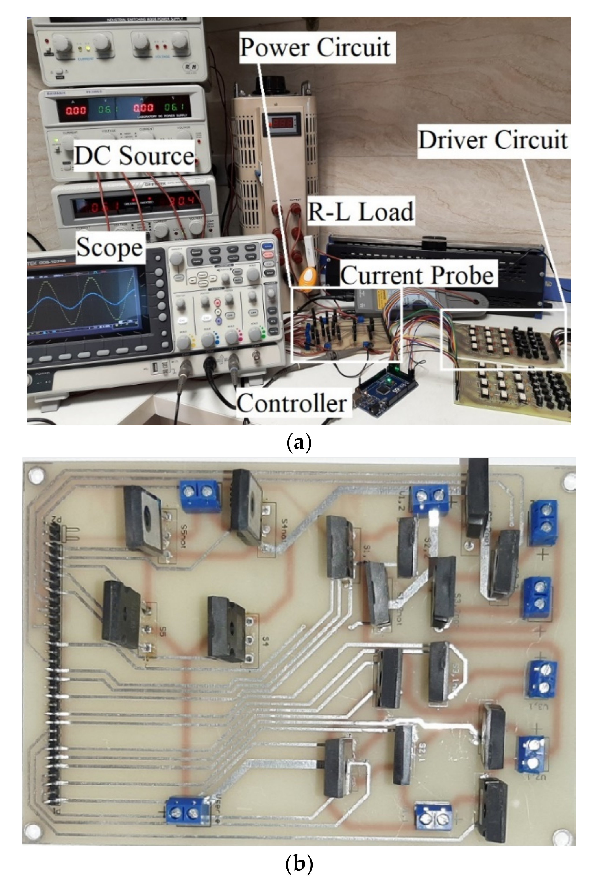
To investigate the performance of the proposed structure, a prototype containing two RSBM is simulated, and a laboratory prototype is implemented. The proposed structure containing two RSBM is investigated for the symmetric and asymmetric topologies. The laboratory sample hardware includes MOSFET IRFP460 power switches. The ARDUINO MEGA2560 microcontroller is used to generate gate pulses, which are isolated and amplified to drive the switches using the TLP250 optocoupler. The laboratory prototype and related instruments are shown in Figure 8.
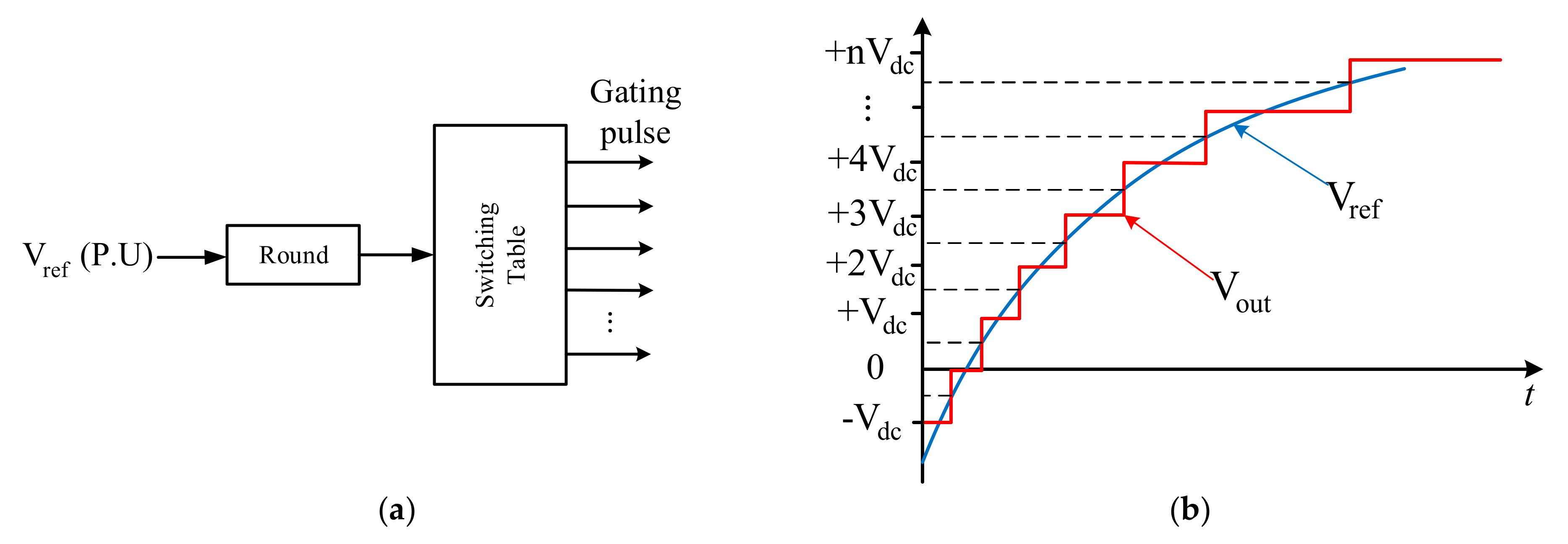
As it is known, multi-level inverter switching methods are classified into two categories according to the switching frequency, which can be low frequency or high frequency, respectively. From the first class it can be mentioned the staircase switching, fundamental frequency switching, active harmonic elimination, nearest level modulation (NLM) and selective harmonic elimination (SHE) technique. The second class includes sinusoidal PWM and space vector modulation (SVM) techniques. The modulation methods in both classes can be easily adapted and implemented to the topology proposed in this paper. The NLM method has been used to generate the switching pulses (see Figure 9a), using an integer that is close to the nearest voltage level as the reference signal. For example, if the voltage is in the range of 1.5 to 2.5, then the reference of 2Vdc will be generated. Figure 9b presents the NLM operation. The switching frequency is not well-known in NLM method. But it is low and is relatively near to output voltage frequency. The output voltage frequency is considered 50 Hz.
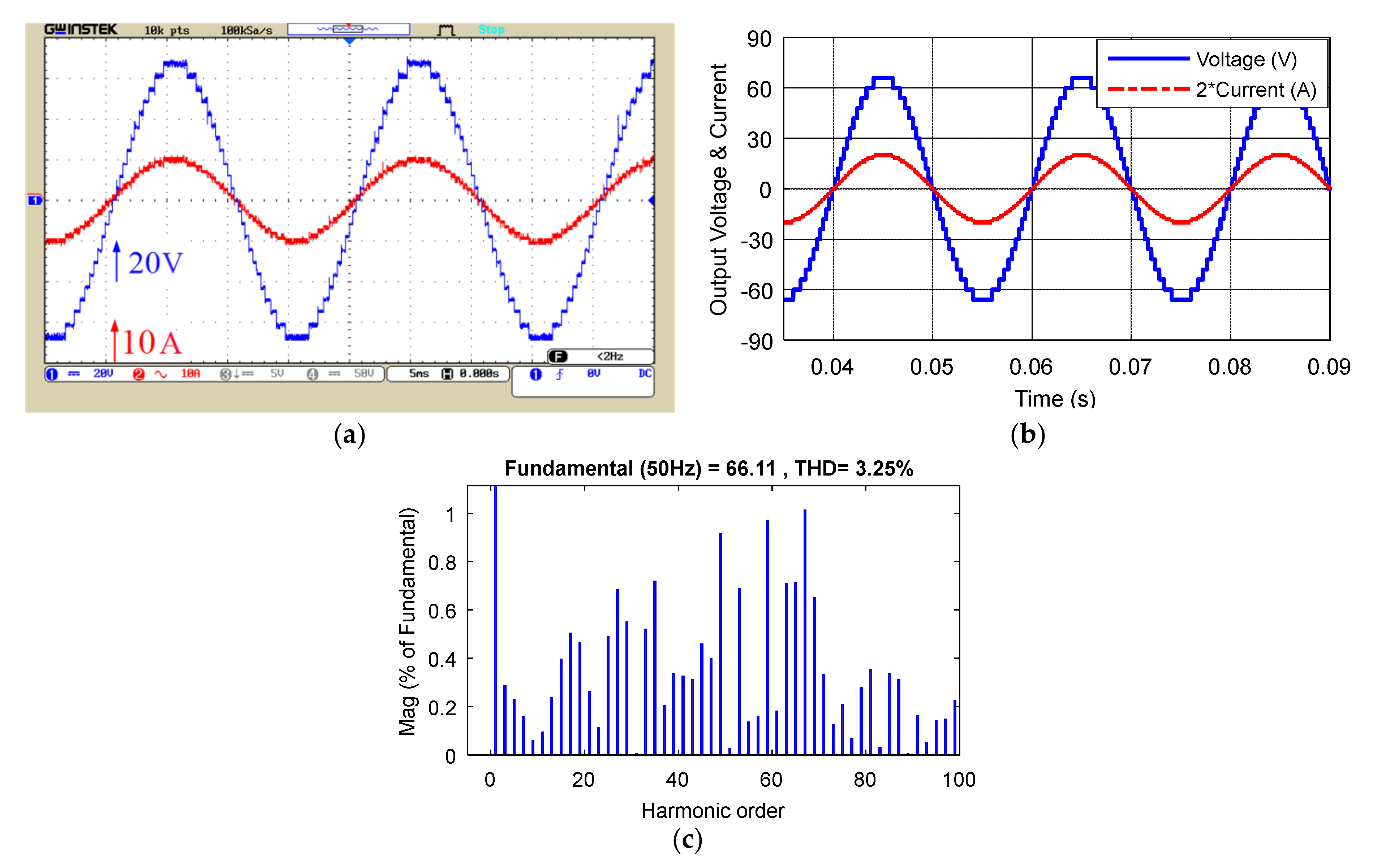
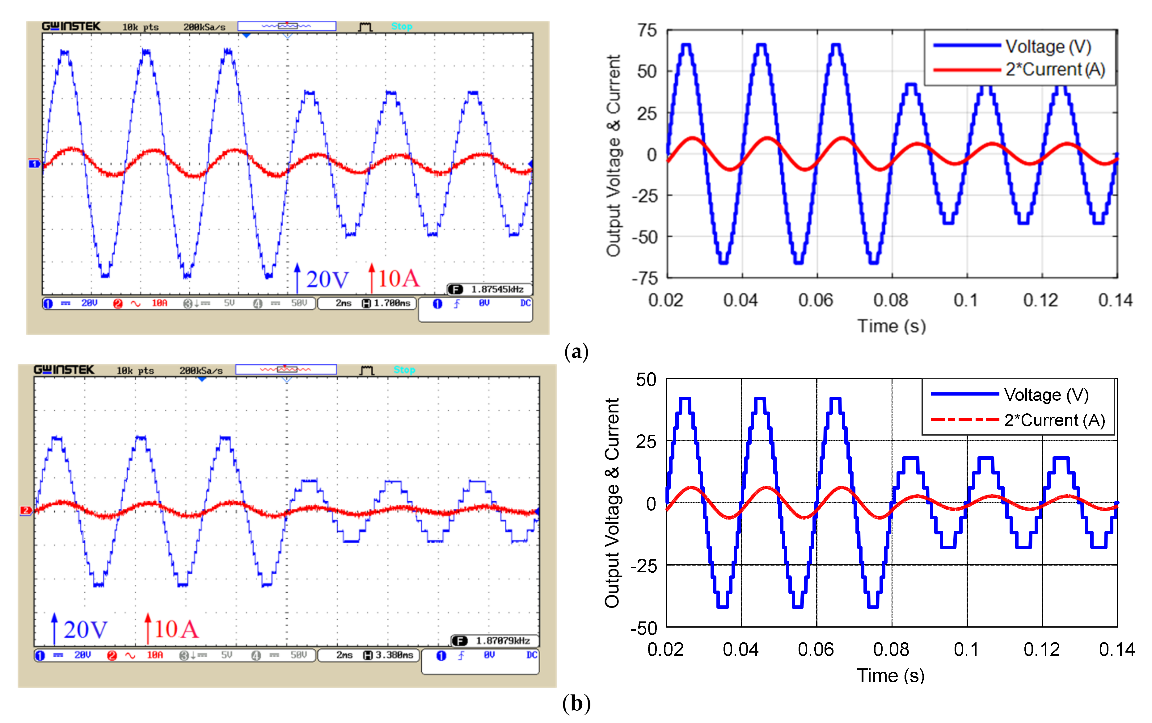
In symmetric topology, the value of DC voltage sources is V0 = V1 = V2 = 6 V. First, the inverter results for a purely resistive load Zload1 = 6.6 Ω are presented in Figure 10. The peak output voltage of the inverter with 11 levels of 6 V steps results in 66 volts. The peak load current, in this case, is 10A. The harmonic spectrum of the proposed topology is presented in Figure 10c, highlighting that the total harmonic distortion (THD) is 3.25%, with advantage in size and cost of the output filter.
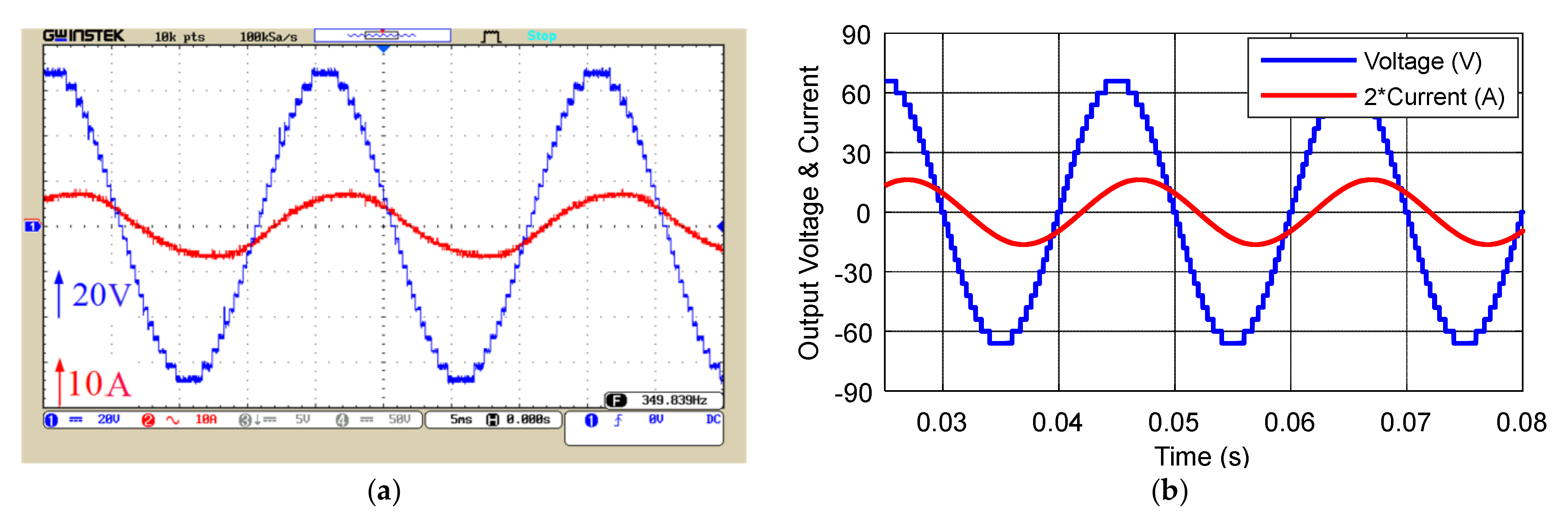
Additionally, Figure 11 displays the results of the proposed structure in the case of symmetric sources for a resistive-inductive load Zload2 = 6.6 + j4.71 Ω. The peak load current in the case of R-L output load is 8.1 A, in which the inductance of the load filters, the current, and the load current is obtained similar to a sine wave.
To analyze and introduce the response of the proposed MLI in a dynamic situation, the modulation index changes abruptly, and the system response is evaluated. It should be noted that, this test is only open loop dynamic responses. As shown in Figure 12, for this purpose, the modulation index is once changed from 1 to 0.65 according to Figure 12a, and again according to Figure 12b, the modulation index is changed from 0.65 to 0.3. The proper performance of the proposed multi-level inverter in dynamic conditions is visible for changing the modulation index in Figure 12.
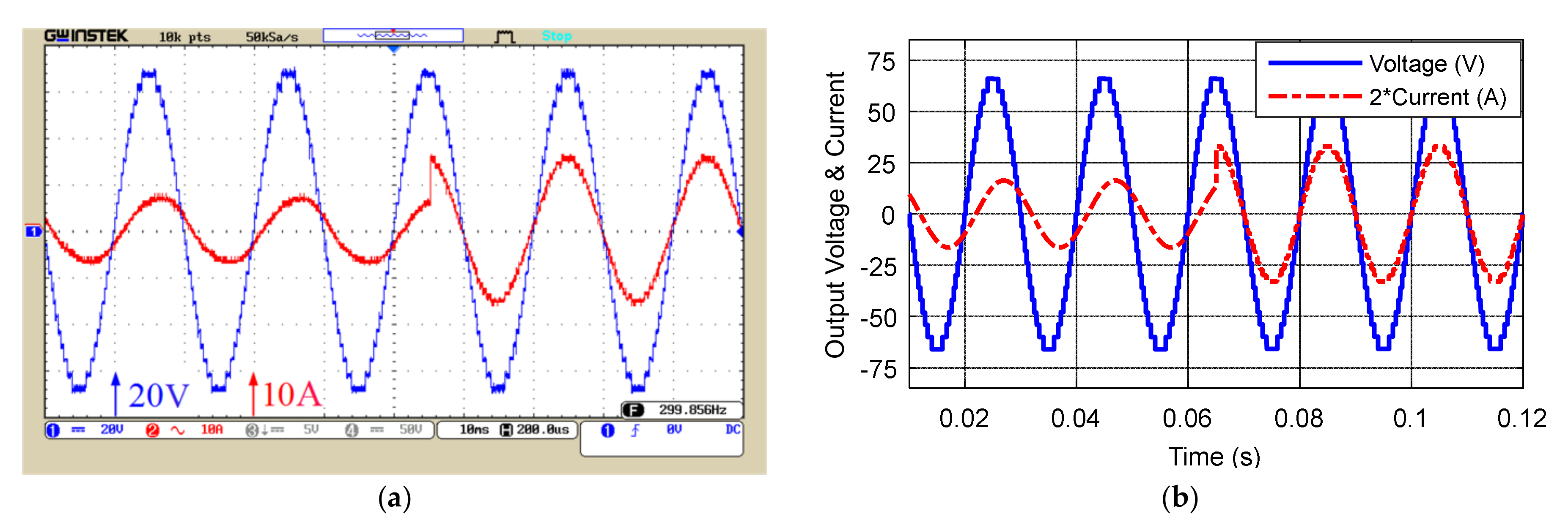
The behavior of the proposed structure for a sudden change in load is evaluated as well. For this purpose, the load changes abruptly from resistive-inductive to pure resistive. Figure 13 illustrates inverter output voltage and current for a sudden change of the resistive-inductive load Zload2 = 6.6 + j4.71 Ω to a purely resistive load Zload3 = 4 Ω. The proposed structure performs well under dynamic load change conditions as well.
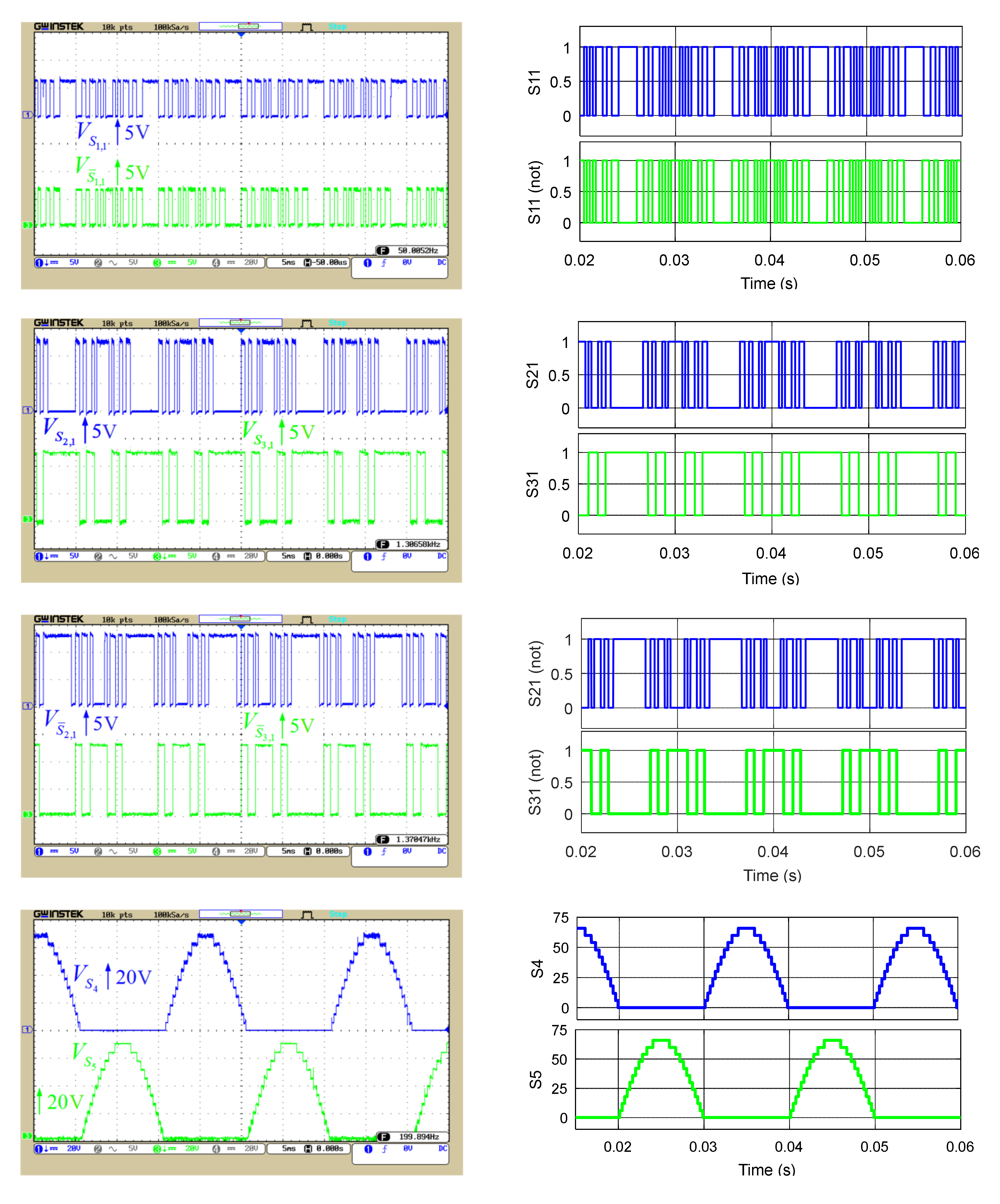
Figure 14 displays the blocking voltage for switches of the proposed structure in the symmetric topology. Based on these curves, the maximum voltage across each switch is determined. These diagrams confirm the correct operation of the proposed structure.
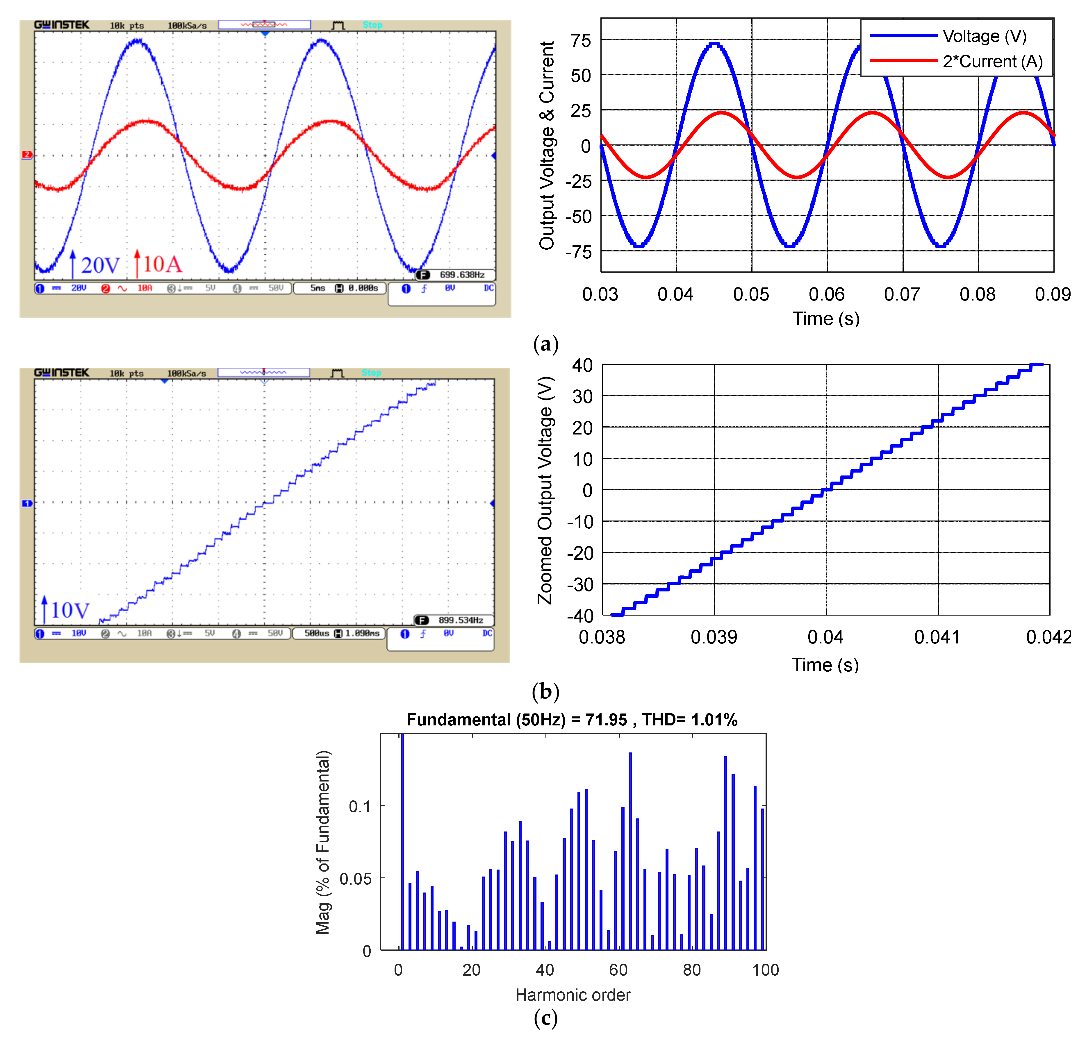
To evaluate the performance of multi-level inverter in asymmetric topology, the value of DC voltage sources is selected based on the proposed fourth algorithm according to Table 2 and assumed as V0 = V1 = 2 V, V2 = 12 V. The performance results of the proposed multi-level inverter with asymmetric topology for a resistive-inductive load are presented in Figure 15. The number of voltage steps increases from 11 levels in the symmetric topology to 36 levels of 2 V steps in the asymmetric topology. In this case, the peak output voltage results in 72 V. The peak load current equals 11.4 A in this condition. Figure 15b displays the zoomed staircase waveform of the output voltage. The proper performance of the proposed structure is clearly shown in this figure in the production of voltage steps. In addition, the THD value is decreased from 3.26% in the symmetric topology to 1.01% in the asymmetric topology. This THD value demonstrates that the asymmetric topology of the suggested MLI can operate properly without any output filter, which results in more reduction in overall size and cost.
Dynamic load testing is necessary to evaluate the capability of the proposed structure in the application of electric motor drives. Based on the simulation results and laboratory results of the prototype, it can be concluded that the performance of the proposed structure is satisfactory, and the proposed topology provides a desirable performance.
6. Conclusions
In this paper, a novel configuration is proposed for multi-level voltage source inverters to reduce the number of switches. The proposed structure uses a reduced switch basic module to generate more output voltage levels. This structure is investigated for symmetric and asymmetric topologies. The efficiency of the structure is presented for different loads and compared with several other structures. The result is shown that the suggested inverter has higher efficiency. Besides, the comparison in terms of circuit devices reveals that the number of switches of the proposed structure is less than other reported structures. This difference in the number of switches is clearly evident at higher levels, and the graph slope of the number of switches to the number of levels is 0.6, which is less than other structures. Also, the number of gate driver, as well as the TBV parameter are in good situation and superior in comparison with most of similar structures. These results make that the proposed structure has a low cost and size. The performance of the proposed structure is confirmed by simulation and laboratory results. In the laboratory prototype, different loading conditions, including resistive load, resistive-inductive load as well as dynamic load, have been used to validate the proposed structure. Modulation index change is also performed for the proposed structure. Results evaluation of simulations and laboratory samples, as well as the results of comparisons, indicate the appropriate performance of the proposed structure.
Author Contributions
Conceptualization, A.S., M.H. and H.S.; methodology, A.S., M.H. and H.S.; software, A.S. and M.H.; validation, M.H. and H.S.; investigation, M.H. and H.S.; resources, N.B.; data curation, N.B.; writing—original draft preparation, A.S., M.H. and H.S.; supervision, H.S. and N.B.; Funding acquisition: N.B.; Visualization: H.S. and N.B.; writing—review and editing: M.H., H.S. and N.B.; project administration, N.B.; Formal analysis: M.H., N.B. and H.S. All authors have read and agreed to the published version of the manuscript.
Funding
This research received no external funding.
Institutional Review Board Statement
Not applicable.
Informed Consent Statement
Not applicable.
Data Availability Statement
Not applicable.
Conflicts of Interest
The authors declare no conflict of interest.
References
- Sunddararaj, S.P.; Srinivasarangan Rangarajan, S. An extensive review of multilevel inverters based on their multifaceted structural configuration, triggering methods and applications. Electronics 2020, 9, 433. [Google Scholar] [CrossRef] [Green Version]
- Ahmed, S.A.M.; Abd El Sattar, M. Dynamic Performance and Effectiveness of Voltage Disturbances on the Improvement of Power Quality for Grid-Connected DFIG System Based Wind Farm. J. Electr. Eng. Electron. Control. Comput. Sci. 2019, 5, 25–30. Available online: https://jeeeccs.net/index.php/journal/article/view/126 (accessed on 3 September 2019).
- Ahmed, S.A.M. Performance Analysis of Power Quality Improvement for Standard IEEE 14-Bus Power System based on FACTS Controller. J. Electr. Eng. Electron. Control Comput. Sci. 2019, 5, 11–18. Available online: https://jeeeccs.net/index.php/journal/article/view/134 (accessed on 3 December 2019).
- Sorlei, I.S.; Bizon, N.; Thounthong, P.; Varlam, M.; Carcadea, E.; Culcer, M.; Iliescu, M.; Raceanu, M. Fuel Cell Electric Vehicles—A Brief Review of Current Topologies and Energy Management Strategies. Energies 2021, 14, 252. [Google Scholar] [CrossRef]
- Benbouhenni, H.; Bizon, N. Improved Rotor Flux and Torque Control Based on the Third-Order Sliding Mode Scheme Applied to the Asynchronous Generator for the Single-Rotor Wind Turbine. Mathematics 2021, 9, 2297. [Google Scholar] [CrossRef]
- Shahzad, U. Significance of Smart Grids in Electric Power Systems: A Brief Overview. J. Electr. Eng. Electron. Control. Comput. Sci. 2020, 6, 7–12. Available online: https://jeeeccs.net/index.php/journal/article/view/141 (accessed on 3 February 2020).
- Onyishi, D.U.; Ofualagba, G. Analysis of the Electricity Distribution Supply in Eastern Nigeria: Current Challenges and Possible Solutions. J. Electr. Eng. Electron. Control Comput. Sci. 2021, 7, 1–8. Available online: https://jeeeccs.net/index.php/journal/article/view/209 (accessed on 3 September 2021).
- Seifi, A.; Hosseinpour, M.; Dejamkhooy, A. A switch-source cell-based cascaded multilevel inverter topology with minimum number of power electronics components. Trans. Inst. Meas. Control 2021, 43, 1212–1225. [Google Scholar] [CrossRef]
- Sarebanzadeh, M.; Hosseinzadeh, M.A.; Garcia, C.; Babaei, E.; Hosseinpour, M.; Seifi, A.; Rodriguez, J. A 15-Level Switched-Capacitor Multilevel Inverter Structure with Self-Balancing Capacitor. IEEE Trans. Circuits Syst. II Express Briefs 2022, 69, 1477–1481. [Google Scholar] [CrossRef]
- Hosseinpour, M.; Seifi, A.; Dejamkhooy, A.; Sedaghati, F. Switch count reduced structure for symmetric bi-directional multilevel inverter based on switch-diode-source cells. IET Power Electron. 2020, 13, 1675–1686. [Google Scholar] [CrossRef]
- Esmaeilzadeh, R.; Ajami, A.; Banaei, M.R. Two-Stage Inverter Based on Combination of High Gain DC-DC Converter and Five-Level Inverter for PV-Battery Energy Conversion. J. Oper. Autom. Power Eng. 2018, 6, 101–110. Available online: http://joape.uma.ac.ir/article_641.html (accessed on 29 February 2018).
- Siddique, M.D.; Mekhilef, S.; Shah, N.M.; Sarwar, A.; Memon, M.A. A new single-phase cascaded multilevel inverter topology with reduced number of switches and voltage stress. Int. Trans. Electr. Energy Syst. 2020, 30, 12191. [Google Scholar] [CrossRef]
- Oskuee, M.R.; Karimi, M.; Ravadanegh, S.N.; Gharehpetian, G.B. An innovative scheme of symmetric multilevel voltage source inverter with lower number of circuit devices. IEEE Trans. Ind. Electron. 2015, 62, 6965–6973. [Google Scholar] [CrossRef]
- Alishah, R.S.; Bertilsson, K.; Vosoughi Kurdkandi, N.; Hosseini, S.H.; Gharehkoushan, A.Z.; Ali, J.S. A New Switched-Ladder Multilevel Converter Structure with Reduced Power Electronic Components. J. Circuits Syst. Comput. 2021, 30, 2150217. [Google Scholar] [CrossRef]
- Jayabalan, M.; Jeevarathinam, B.; Sandirasegarane, T. Reduced switch count pulse width modulated multilevel inverter. IET Power Electron. 2017, 10, 10–17. [Google Scholar] [CrossRef]
- Ponraj, R.P.; Sigamani, T.; Subramanian, V. A developed H-bridge cascaded multilevel inverter with reduced switch count. J. Electr. Eng. Technol. 2021, 16, 1445–1455. [Google Scholar] [CrossRef]
- Peddapati, S. A generalized symmetrical MLI topology with improved commutation. Electr. Eng. 2020, 102, 2617–2635. [Google Scholar] [CrossRef]
- Siddique, M.D.; Mekhilef, S.; Shah, N.M.; Memon, M.A. Optimal design of a new cascaded multilevel inverter topology with reduced switch count. IEEE Access 2019, 7, 24498–24510. [Google Scholar] [CrossRef]
- Samsami, H.; Taheri, A.; Samanbakhsh, R. New bidirectional multilevel inverter topology with staircase cascading for symmetric and asymmetric structures. IET Power Electron. 2017, 10, 1315–1323. [Google Scholar] [CrossRef]
- Dhanamjayulu, C.; Meikandasivam, S. Implementation and comparison of symmetric and asymmetric multilevel inverters for dynamic loads. IEEE Access 2017, 6, 738–746. [Google Scholar] [CrossRef]
- Gohari, A.; Afjei, E.S.; Torkaman, H. Novel symmetric modular hybrid multilevel inverter with reduced number of semiconductors and low-voltage stress across switches. IEEE J. Emerg. Sel. Top. Power Electron. 2019, 8, 4297–4305. [Google Scholar] [CrossRef]
- Alishah, R.S.; Hosseini, S.H.; Babaei, E.; Sabahi, M. A new general multilevel converter topology based on cascaded connection of submultilevel units with reduced switching components, DC sources, and blocked voltage by switches. IEEE Trans. Ind. Electron. 2016, 63, 7157–7164. [Google Scholar] [CrossRef]
- Hosseinpour, M.; Seifi, A.; Rahimian, M.M. A bidirectional diode containing multilevel inverter topology with reduced switch count and driver. Int. J. Circuit Theory Appl. 2020, 48, 1766–1785. [Google Scholar] [CrossRef]
- Hosseini Montazer, B.; Olamaei, J.; Hosseinpour, M.; Mozafari, B. A generalized diode containing bidirectional topology for multilevel inverter with reduced switches and power loss. Int. J. Circuit Theory Appl. 2021, 49, 2959–2978. [Google Scholar] [CrossRef]
- Selvaraj, S.; Kumaresan, G.; Sathik, M.A. Modified “K”-type multilevel inverter topology with reduced switches, DC sources, and power loss. Int. Trans. Electr. Energy Syst. 2020, 30, 12345. [Google Scholar] [CrossRef]
- Meraj, S.T.; Hasan, K.; Masaoud, A. A novel configuration of cross-switched T-type (CT-type) multilevel inverter. IEEE Trans. Power Electron. 2019, 35, 3688–3696. [Google Scholar] [CrossRef]
- Ponraj, R.P.; Sigamani, T. A novel design and performance improvement of symmetric multilevel inverter with reduced switches using genetic algorithm. Soft Comput. 2021, 25, 4597–4607. [Google Scholar] [CrossRef]
- Lee, S.S.; Sidorov, M.; Idris, N.R.; Heng, Y.E. A symmetrical cascaded compact-module multilevel inverter (CCM-MLI) with pulsewidth modulation. IEEE Trans. Ind. Electron. 2017, 65, 4631–4639. [Google Scholar] [CrossRef]
- Siddique, M.D.; Mekhilef, S.; Shah, N.M.; Sarwar, A.; Iqbal, A.; Memon, M.A. A new multilevel inverter topology with reduce switch count. IEEE Access 2019, 7, 58584–58594. [Google Scholar] [CrossRef]
- Ali, J.S.; Alishah, R.S.; Krishnasamy, V. A new generalized multilevel converter topology with reduced voltage on switches, power losses, and components. IEEE J. Emerg. Sel. Top. Power Electron. 2018, 7, 1094–1106. [Google Scholar] [CrossRef]
- Seifi, A.; Hosseinpour, M.; Dejamkhooy, A.; Sedaghati, F. Novel reduced switch-count structure for symmetric/asymmetric cascaded multilevel inverter. Arab. J. Sci. Eng. 2020, 45, 6687–6700. [Google Scholar] [CrossRef]
Figure 1.
(a) The suggested RSBM, (b) , (c) , (d) , (e) , (f) , (g) .

Figure 2.
The proposed generalized inverter structure.

Figure 3.
The proposed cascaded topology.

Figure 4.
(a) Power losses and efficiency curves for the proposed 11-level basic cell topology at three types of loads, (a) Conduction losses, (b) Switching losses, (c) Temperature of switches, (d) Efficiency and total losses.
Figure 4.
(a) Power losses and efficiency curves for the proposed 11-level basic cell topology at three types of loads, (a) Conduction losses, (b) Switching losses, (c) Temperature of switches, (d) Efficiency and total losses.


Figure 5.
Efficiency comparison of the proposed 11-level basic cell with other topologies. [A] Alishah et al., 2021, [B] Jayabalan et al., 2017, [C] Ponraj et al., 2021.
Figure 5.
Efficiency comparison of the proposed 11-level basic cell with other topologies. [A] Alishah et al., 2021, [B] Jayabalan et al., 2017, [C] Ponraj et al., 2021.

Figure 6.
Comparative diagrams including: (a) NIGBT/NL, (b) NGD/NL. [A] Oskuee et al., 2015, [B] Alishah et al., 2021, [C] Jayabalan et al., 2017, [D] Ponraj et al., 2021, [E] Peddapati 2020, [F] Siddique et al., 2019, [G] Samsami et al., 2017, [H] Dhanamjayulu et al., 2017, [I] Gohari et al., 2019, [J] Alishah et al., 2016, [K] Hosseinpour et al., 2020, [L] Hosseini Montazer et al., 2021, [M] Selvaraj et al., 2020, [N] Meraj et al., 2019, [O] Ponraj et al., 2021, [P] Lee et al., 2017, [Q] Siddique et al., 2019, [R] Ali 2018, [S] Seifi et al., 2020.

Figure 7.
TBV/NL diagram for the proposed structure and other structures.* Indicates product symbol. [A] Oskuee et al., 2015, [B] Alishah et al., 2021, [C] Jayabalan et al., 2017, [D] Ponraj et al., 2021, [E] Peddapati 2020, [F] Siddique et al., 2019, [G] Samsami et al., 2017, [H] Dhanamjayulu et al., 2017, [I] Gohari et al., 2019, [J] Alishah et al., 2016, [K] Hosseinpour et al., 2020, [L] Hosseini Montazer et al., 2021, [M] Selvaraj et al., 2020, [N] Meraj et al., 2019, [O] Ponraj et al., 2021, [P] Lee et al., 2017, [Q] Siddique et al., 2019, [R] Ali 2018, [S] Seifi et al., 2020.

Figure 8.
(a) A laboratory prototype of the proposed structure, (b) The power circuit of proposed structure.
Figure 8.
(a) A laboratory prototype of the proposed structure, (b) The power circuit of proposed structure.

Figure 9.
(a) NLM method, (b) The NLM operation.

Figure 10.
The waveforms for resistive output load in symmetric topology, (a) laboratory sample voltage and current, (b) simulation voltage and current, (c) output voltage THD. * Indicates product symbol.
Figure 10.
The waveforms for resistive output load in symmetric topology, (a) laboratory sample voltage and current, (b) simulation voltage and current, (c) output voltage THD. * Indicates product symbol.

Figure 11.
Resistive-inductive load waveforms in symmetric topology, (a) laboratory sample voltage and current, (b) simulation voltage and current. * Indicates product symbol.
Figure 11.
Resistive-inductive load waveforms in symmetric topology, (a) laboratory sample voltage and current, (b) simulation voltage and current. * Indicates product symbol.

Figure 12.
Voltage and current waveforms for changes of the modulation index: (a) from 1 to 0.65 and (b) from 0.65 to 0.3. * Indicates product symbol.
Figure 12.
Voltage and current waveforms for changes of the modulation index: (a) from 1 to 0.65 and (b) from 0.65 to 0.3. * Indicates product symbol.

Figure 13.
Voltage and current waveforms related to load’s dynamic change, (a) laboratory result, (b) simulation result. * Indicates product symbol.
Figure 13.
Voltage and current waveforms related to load’s dynamic change, (a) laboratory result, (b) simulation result. * Indicates product symbol.

Figure 14.
Blocking voltage of the proposed structure switches for symmetric topology.

Figure 15.
The waveforms of Proposed MLI in asymmetric topology (a) voltage and current, (b) zoomed voltage, (c) output voltage THD. * Indicates product symbol.
Figure 15.
The waveforms of Proposed MLI in asymmetric topology (a) voltage and current, (b) zoomed voltage, (c) output voltage THD. * Indicates product symbol.


Table 1.
The switching logic of the RSBM.
| S3 | Vout | ||
|---|---|---|---|
| 1 | 0 | 1 | 0 |
| 0 | 0 | 1 | Vdc |
| 1 | 1 | 1 | 2Vdc |
| 0 | 1 | 1 | 3Vdc |
| 1 | 1 | 0 | 4Vdc |
| 0 | 1 | 0 | 5Vdc |
Table 2.
Proposed algorithms for asymmetric topology voltage source size.
| Proposed Algorithm | Magnitude of dc Voltage Sources | NIGBT | NL | ND |
|---|---|---|---|---|
| 1st proposed algorithm | ||||
| 2nd proposed algorithm | ||||
| 3rd proposed algorithm | ||||
| 4th proposed algorithm |
Table 3.
Comparing the parameters of the proposed topology with other basic topologies.
| NIGBT | NGD | NL | NDC | TBV(* Vdc) | ND | NIGBT,ON | NIGBT/NL | |
|---|---|---|---|---|---|---|---|---|
| [13] | 10 | 10 | 9 | 4 | 22 | 0 | 5 | 1.11 |
| [14] | 12 | 10 | 9 | 4 | 24 | 0 | 7 | 1.33 |
| [15] | 12 | 9 | 7 | 3 | 18 | 0 | 7 | 1.71 |
| [16] | 10 | 10 | 7 | 3 | 20 | 0 | 5 | 1.42 |
| [17] | 10 | 7 | 7 | 3 | 21 | 1 | 4 | 1.42 |
| [18] | 8 | 7 | 7 | 3 | 14 | 0 | 4 | 1.14 |
| [19] | 8 | 7 | 7 | 3 | 18 | 0 | 4 | 1.14 |
| [20] | 5 | 5 | 3 | 2 | 9 | 4 | 2 | 1.66 |
| [21] | 6 | 6 | 7 | 4 | 12 | 0 | 3 | 0.85 |
| [22] | 12 | 10 | 9 | 4 | 24 | 0 | 7 | 1.33 |
| [23] | 11 | 10 | 11 | 5 | 31 | 1 | 5 | 1 |
| [24] | 11 | 10 | 11 | 5 | 31 | 2 | 4 | 1 |
| [25] | 8 | 8 | 7 | 3 | 12 | 0 | 3 | 1.14 |
| [26] | 10 | 8 | 9 | 4 | 20 | 0 | 4 | 1.11 |
| [27] | 10 | 10 | 9 | 4 | 20 | 0 | 5 | 1.11 |
| [28] | 10 | 7 | 7 | 3 | 20 | 0 | 3 | 1.42 |
| [29] | 10 | 9 | 7 | 3 | 14 | 0 | 4 | 1.42 |
| [30] | 10 | 9 | 9 | 4 | 18 | 0 | 4 | 1.11 |
| [31] | 9 | 9 | 9 | 4 | 22 | 1 | 5 | 1 |
| Proposed | 10 | 10 | 13 | 5 | 30 | 0 | 5 | 0.77 |
* Indicates product symbol.
Publisher’s Note: MDPI stays neutral with regard to jurisdictional claims in published maps and institutional affiliations. |
© 2022 by the authors. Licensee MDPI, Basel, Switzerland. This article is an open access article distributed under the terms and conditions of the Creative Commons Attribution (CC BY) license (https://creativecommons.org/licenses/by/4.0/).
Share and Cite
MDPI and ACS Style
Shayeghi, H.; Seifi, A.; Hosseinpour, M.; Bizon, N. Developing a Generalized Multi-Level Inverter with Reduced Number of Power Electronics Components. Sustainability 2022, 14, 5545. https://0-doi-org.brum.beds.ac.uk/10.3390/su14095545
AMA Style
Shayeghi H, Seifi A, Hosseinpour M, Bizon N. Developing a Generalized Multi-Level Inverter with Reduced Number of Power Electronics Components. Sustainability. 2022; 14(9):5545. https://0-doi-org.brum.beds.ac.uk/10.3390/su14095545
Chicago/Turabian StyleShayeghi, Hossein, Ali Seifi, Majid Hosseinpour, and Nicu Bizon. 2022. "Developing a Generalized Multi-Level Inverter with Reduced Number of Power Electronics Components" Sustainability 14, no. 9: 5545. https://0-doi-org.brum.beds.ac.uk/10.3390/su14095545
Note that from the first issue of 2016, this journal uses article numbers instead of page numbers. See further details here.