Article

H-Terminated Diamond Surface Band Bending Characterization by Angle-Resolved XPS

1
Dpto. Ciencia de los Materiales e IM y QI, Facultad de Ciencias, Universidad de Cádiz, 11510 Puerto Real (Cádiz), Spain
2
Univ. Grenoble Alpes, CNRS, Grenoble INP*, Institut Néel, 38000 Grenoble, France
3
Dpto. Química-Física, Facultad de Ciencias, Universidad de Cádiz, 11510 Puerto Real (Cádiz), Spain
*
Author to whom correspondence should be addressed.
Submission received: 2 February 2020 / Revised: 13 February 2020 / Accepted: 14 February 2020 / Published: 18 February 2020

Abstract

:
Concerning diamond-based electronic devices, the H-terminated diamond surface is one of the most used terminations as it can be obtained directly by using H2 plasma, which also is a key step for diamond growth by chemical vapour deposition (CVD). The resultant surfaces present a p-type surface conductive layer with interest in power electronic applications. However, the mechanism for this behavior is still under discussion. Upward band bending due to surface transfer doping is the most accepted model, but has not been experimentally probed as of yet. Recently, a downward band bending very near the surface due to shallow acceptors has been proposed to coexist with surface transfer doping, explaining most of the observed phenomena. In this work, a new approach to the measurement of band bending by angle-resolved X-ray photoelectron spectroscopy (ARXPS) is proposed. Based on this new interpretation, a downward band bending of 0.67 eV extended over 0.5 nm was evidenced on a (100) H-terminated diamond surface.

Graphical Abstract

1. Introduction

Diamond exhibits very interesting bulk properties such as a wide band-gap of 5.5 eV, a high thermal conductivity >20 W/cm, and a high breakdown field of 10 MV/cm [1,2], which makes it proper for high power and high-frequency electronic applications. Unipolar electronic devices such as diodes or transistors are awakening a great interest, but its electronic performance has been demonstrated to be very sensitive to surface terminations. Up to now, H- and O-terminated surfaces are the most frequently used for diamond power devices reported in the literature [2,3,4,5,6,7,8,9,10]. H-terminated diamond (H-diamond) has been extensively used for MOSFETs and Schottky barrier diodes. For the latter, H-diamond based diodes have been demonstrated to have lower Schottky barrier height values in comparison to that of O-diamond based Schottky diodes. Concerning MOSFETs, most of the results are obtained on H-diamond, where the device works normally in the on-state due to the surface conductive layer (SCL). The off-state can be reached by depleting the carriers by field effect. The reasons for such phenomena are that terminations affect the diamond surface band bending.
In order to obtain H-diamond, H2 plasma is the most frequently used treatment as it forms part of the diamond CVD growth process. Thus, (100)-H-diamond surfaces present a (2 × 1) reconstruction pattern [11] that consists of carbon–carbon surface dimers in which a hydrogen adatom is bonded to each carbon. One of the more controversial properties of this termination is the appearance of a p-type SCL with a carrier density up to ~1013 cm−2. This conductivity can vary by exposing the surface to different ambients [12] and has been related to surface roughness [13].
The surface transfer doping (STD) model, in which electrons from diamond valence band can be transferred to surface adsorbents or defects related energy levels, is up to now the most accepted mechanism to explain SCL [14,15,16]. In the STD model, the Fermi level of the surface related energy levels lies deeper than that of bulk diamond. An upward band bending and, hence, a hole accumulation layer is created at thermal equilibrium, explaining the 2D-hole gas. However, this upward band bending has not been empirically observed. Additionally, some experimental evidence cannot be explained by the STD model and, thus, it requires the exploration of new mechanisms that fit all the observations, and some researchers are considering other possibilities. In this sense, a downward band bending in the very near surface of the (100)-H-diamond has been recently found [17,18], which could be related to shallow acceptors contributing to the SCL. This idea is supported by the observation of a hydrogen subsurface contribution of a few monolayers [16,19] as well as the stability of hydrogen in the C–C bond-center sites of diamond [20,21]. The combination of the two models: STD to explain an upward band bending and the accumulation layer, and surface shallow acceptors due to the presence of hydrogen to explain a downward band bending at the very near surface can explain most of the SCL observed phenomena. In any case, the mechanism is still under discussion and new observations are needed before obtaining clear conclusions.
The X-ray photoelectron spectroscopy (XPS) technique has been widely employed for studying diamond chemical terminations [22,23,24,25,26,27], but the interpretation of the peaks are still controversial. The detection of the H-diamond surface downward band bending was supported by ARXPS experiments that, on the other hand, are rarely found in the literature. By varying the polar angle, ARXPS can be more surface sensitive than conventional XPS, allowing the study of the effects occurring along the sample depth axis in the outermost nanometers of the sample. Band bending is commonly characterized by a shift observation of a core-level maximum peak from the Fermi level. In the case of diamond, this core-level is the C 1s and the position of the Fermi level is obtained from a metallic energy reference (e.g., gold) or by C 1s calibration [28]. A depth profile of the positions of the maximum C 1s peak for different polar angles is used to characterize the surface band bending potential Vbb. This method is widely used in the literature, but can have strong limitations, for example, in the case of a very short band bending width, d. In such cases, most of the detected signal will be related to the bulk of the sample and a shift of the sample main core-level maximum peak can hardly be detected. Furthermore, the band bending width would remain unknown by this method.
In this work, to overcome such limitations, a new approach to the measurement of band bending by ARXPS is described and used to explain spectra contributions in a (100)-oriented H-diamond surface. First, a theoretical model approximation for the shape of an XPS band bending contribution is described in Section 3.1. Then, this band bending shape is considered for the deconvolution of ARXPS C 1s spectra using a simple model described in Section 3.2. From the fit of the experimental data to the proposed model, a downward band bending component is characterized in terms of Vbb and d.

2. Materials and Methods

For this experiment, a 3 × 3 mm2 diamond (100)-oriented type IIa substrate from the NDT company (Saint Petersburg, Russia) was used. Diamond suppliers commonly apply a polishing step that results in a surface roughness too high to be considered for this experiment. In order to get a flatter and more homogeneous surface, as received substrates were submitted to an extra polishing step. Surface morphology was evaluated by atomic force microscopy before and after this polishing process in an AFM-VEECO-NSIV system (VEECO, New York, NY, USA) working in tapping mode. Several measurements were carried out in a central region of the sample by using a 5 × 5 μm window each time. Gwyddion software has been used for data analysis [29]. From the combined analysis of all recorded measurements, surface roughness parameters Rq = 0.2 nm and Ra = 0.13 nm were deduced, where Rq is the root mean square and Ra is the arithmetical mean deviation. The surface was analogously again evaluated after H2 plasma, showing a final Rq = 0.1 nm and Ra = 0.09 nm.
The cleaning process was as follows. First, it was immersed in a hot acid mixture of HClO4:HSO4:HNO3 (1:3:4) for 2 h. The temperature of the heating platform was adjusted to 450 °C. Then, it was consecutively submitted to an acetone, ethanol, and isopropanol ultrasound bath for 5 min each. Finally, the substrate was dried by Ar gas flow and stored in room conditions.
H2 plasma was performed in a NIRIM type reactor using a microwave power of 260 W, at a pressure of 30 Torr, a gas H2 flow of 200 sccm, and a temperature of ~800 °C for 2 h.
ARXPS spectra were carried out in a Kratos Axis Ultra DLD spectrometer (Kratos analytical, Manchester, UK) at ultra high vaccum and room temperature with an Al-kα radiation source (1486.6 eV) with an accuracy of 0.1 eV and an energy pass of 20 eV. Spectra were recorded for electron polar angles of θ = 0°, 45°, 70°, and 80° with respect to the surface normal so that the higher the polar angle, the more surface sensitive the measurement is, since the depth from which the electron can escape is reduced by cosθ (Figure 1). In this system, the stage needs to be tilted in order to achieve the required polar angle. The angle between the X-ray beam and the detection column remains constant. A charge neutralizer based on a flood gun of low-energy electrons was used in order to avoid charge effects.
The background was subtracted using the Tougaard model [30]. Peak deconvolution was carried out in MATLAB R2018b software (The MathWorks, Inc., Natick, MA, USA).

3. Results

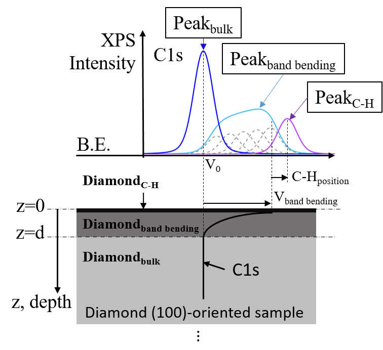
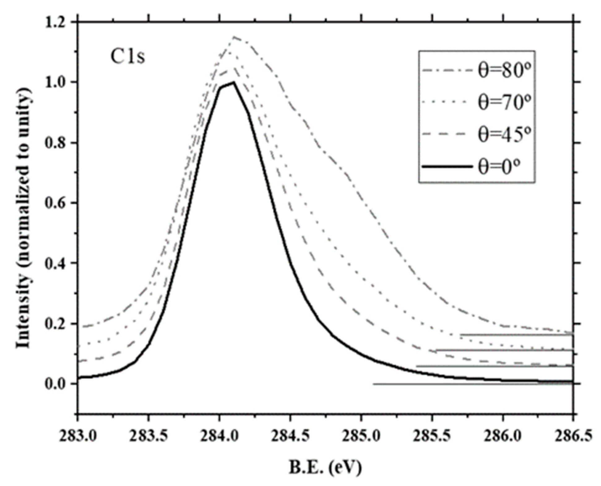
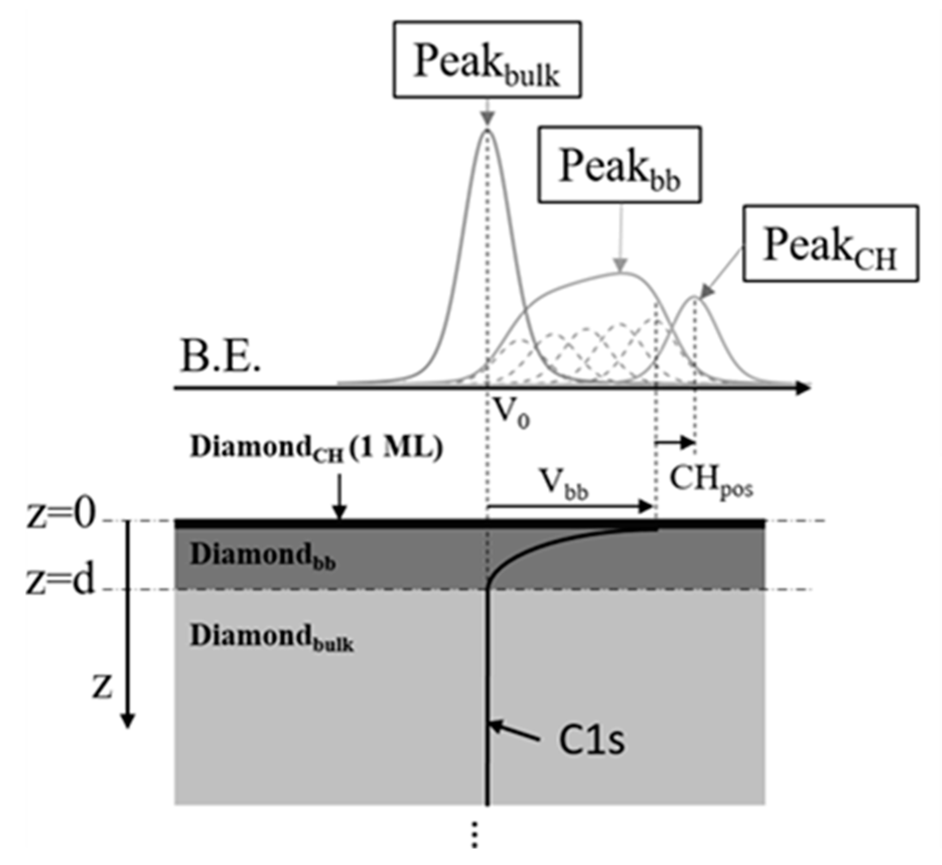
3.1. Shape Generation of a Band Bending XPS Contribution

XPS spectra represent the intensity in electron counts corresponding to each energy level. To describe the XPS contribution of electrons escaping from a fixed energy level, the Voigt distribution is commonly used. It is defined as the convolution of a mixed Gaussian–Lorentzian distribution where the Lorentzian component is related to the lifetime broadening of electrons [31]. However, when a band bending exists and hence all energy-levels bend accordingly, the contribution should be different than a Voigt distribution. In this section, a theoretical approach was obtained for the distribution of a band bending contribution in XPS. The result was applied to the H-diamond C 1s ARXPS spectra in Section 3.2.
To start, the intensity of a certain XPS contribution is commonly described theoretically as:
I 1 ( z ) = K · T · N 1 · σ K e z λ · cos θ d z P ( z )
where T is the analyzer transmission; N 1 is the density of atoms per volume unity; σ is the photoionization cross-section; z is the depth measured from surface; λ is the attenuation length or inelastic mean free path; θ is the polar angle with respect to the surface normal; and K is a constant representing other factors that are supposed to remain constant during the experiment as the photon flux. The exponential term P(z) inside the integral is the Beer–Lambert law, describing the inelastic electron escape probability. In the case of a homogeneous material composed by a single type of element as diamond, Equation (1) can be simplified since T, N 1 , σ , and λ can be considered as constants for the C 1s core-level:
I 1 ( z ) = K · e z λ · cos θ d z
If two contributions are considered, one is related to the band bending region ( I 1 ), for z ∈ [0, d], and the other is related to the bulk region ( I 2 ), for z ∈ [d, ∞), then the intensity ratio is calculated as:
I 1 ( z ) I 2 ( z ) = K · 0 d e z λ · cos θ K · d e z λ · cos θ = 0 d e z λ · cos θ dz d e z λ · cos θ dz = N I ( z )
Since λ can be considered constant for the same material, the intensity ratio NI(z) is only dependent on respective z ranges and XPS polar angle θ .
On the other hand, the band bending curvature along the z-axis, V(z), is described by a solution of Poisson’s Equation:
d 2 V d z 2 = ρ ( z ) ϵ 0 ϵ
where ρ ( z ) is the charge density distribution; ϵ 0 is the vacuum permittivity; and ϵ is the relative permittivity of diamond. A simple solution of this equation, known as the Schottky approximation, is possible when band bending maximum potential, Vbb, significantly exceeds kT (kT = 0.0259 eV at 300 K). Then, the z-dependence of the space charge density ρ can be approximated by a step function. Assuming that a negative charge is homogeneously distributed in the range of z ∈ [0, d] with a charge density N , the Poisson’s equation becomes:
d 2 V d z 2 = e N ϵ 0 ϵ
By integrating twice, V(z) is obtained as:
V ( z ) = V 0 + e N ϵ 0 ϵ ( z d ) 2   z [ 0 , d ]
where V 0 is the bulk potential for z d . This equation can be written in terms of maximum potential Vbb by obtaining the N value from the V(0) expression, then:
V ( z ) = V 0 + V b b d 2 ( z d ) 2   z [ 0 , d ]
It must be noted that this simplification is required as a first approximation due to the absence of scientific evidence about the charge distribution in SCL.
Now, P(z) and V(z) expressions can be put together, describing a curve of parametric equations:
{ Z = z P = e z λ c o s θ   { z [ 0 , d ] } V = V 0 + V b b d 2 ( z d ) 2   { z [ 0 , d ] } }
The projection of this curve on the P–V plane can be obtained by substitution:
V = V 0 + V b b d 2 ( z d ) 2   z = d ( V V 0 ) d 2 V b b P ( V ) = e ( V V 0 ) d 2 V b b d λ c o s θ
This new curve represents the dependence of the electron escape probability on its potential.
Finally, the shape of a band bending contribution in XPS can be understood as the convolution of a Voigt distribution over the probability of escape P(V) in Equation (4). For this purpose, the discrete convolution is used and the numerical approximation was carried out in MATLAB R2018b. The higher the number of points of discrete signals, the better the band bending shape can be approximated. In this approximation, the presence of band bending generates an asymmetric XPS peak with a higher intensity toward the band bending direction that becomes more remarkable for higher Vbb values. A representation of all the curves required for the generation of a band bending XPS contribution is shown in Figure 2.

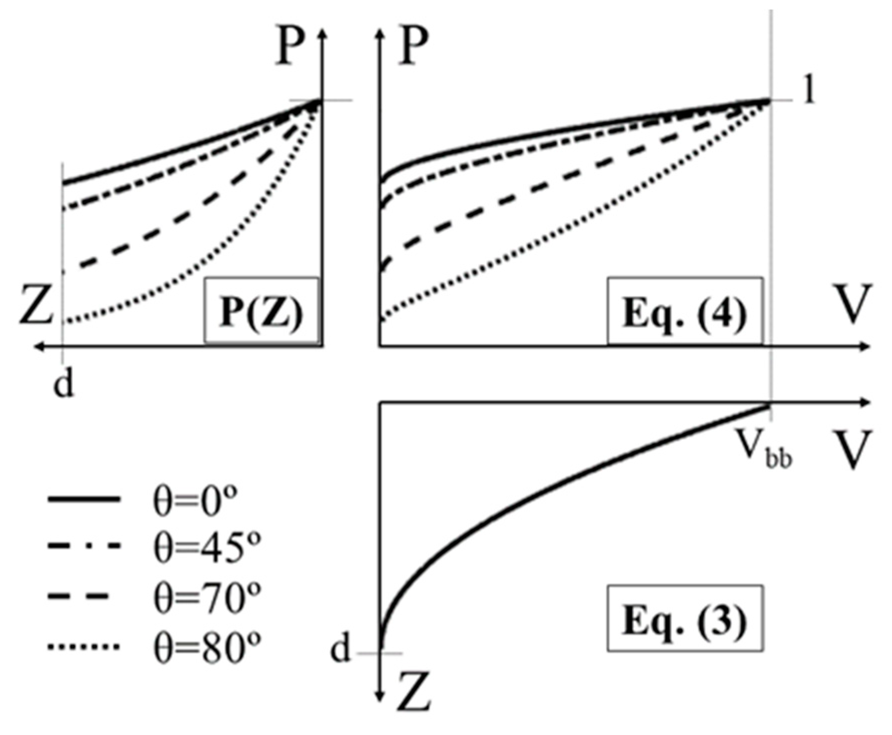
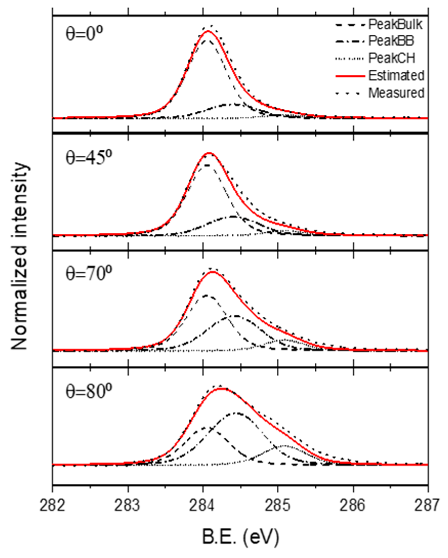
3.2. Surface Band Bending Estimation

The measured (100) H-diamond ARXPS C 1s spectra for θ = 0°, 45°, 70°, and 80° are shown in Figure 3. By using λ, it is possible to calculate the escape probability P(z) curve for selected polar angles θ = 0°, 45°, 70°, and 80° (see Equation (1)) and, thus, the sensitivity depth can be estimated. Since P(z) follows an exponential decay with depth z, the sensitivity depth can be represented by the z value for P(z) < 99%, that is 11.05, 7.81, 3.78, and 1.91 nm for θ = 0°, 45°, 70°, and 80°, respectively. However, it must be noticed that most of the signal is due to quite lower z values. Thus, the z value for P(z) < 50% can be attributed to 1.66, 1.17, 0.56, and 0.28 nm for θ = 0°, 45°, 70° and 80°, respectively. The position of the diamond bulk contribution is expected to be at the maximum peak of the C 1s spectrum at θ = 0°, since in that case, most of the signal should come from the fixed bulk C 1s level. Thus, the diamond C 1s bulk contribution was found at 284.05 eV, which is very similar to previous results [28]. On the other hand, C 1s spectrum at θ = 0° appeared asymmetric with a tail toward a higher B.E. As θ increases, it is clear that this tail becomes a higher contribution with increasing intensity with respect to the bulk contribution. This indicates the surface nature of this second contribution. The position of the maximum C 1s peak moves toward a higher B.E. very slightly for increasing θ values. Very similar behavior has previously been observed by S. Kono et al. [18].
As a preliminary deconvolution, the C 1s spectra were decomposed into two contributions, bulk and surface, by using Voigt distributions (not shown here). The full width at half maximum (FWHM) of the bulk contribution can be estimated in the θ = 0° spectrum since it is the dominant contribution. Then, the FWHM of the surface contribution was obtained as 30% higher than that of the bulk. Finally, all spectra were decomposed by considering the estimated bulk and surface FWHM relation. After that, the surface contribution width, d, was deduced by evaluating the bulk and surface XPS peak intensities by Equation (2). The estimated value of the ~10 monolayers (1 ML = 0.089 nm for (100)-diamond) was too high to be explained only by surface C–H. In this sense, the (100) H-diamond ARXPS C 1s spectra in [18] were very similar to that of Figure 3. The reproducibility of this peak, even for different methodologies, raises doubt about the attribution to surface contamination or defects. Additionally, in conventional XPS experiments on diamond, a tail toward higher B.E. has been routinely attributed to C–H, which somehow supports the idea about the high reproducibility and energy position of this contribution with respect to the diamond bulk contribution in H-terminated (100)-oriented diamond. On the other hand, surface contribution shifted toward higher B.E. with respect to bulk contribution with increasing θ, which makes no sense for contributions with fixed energy levels such as defects.
The presence of a downward band bending XPS contribution as described in Section 3.1. explains the observed spectra. First, because in this case, the intensity of the contribution will depend on the band bending width, explaining this ~10 mL, and second, because the shape of a downward band bending XPS contribution, as shown in Section 3.1., is asymmetric toward higher B.E. and thus, a shift toward higher B.E. as θ increases is expected. Thus, it explains the observed shift of surface contribution as well as the shift of maximum of C 1s spectra.
Assuming the existence of a downward band bending contribution, the recorded spectra was decomposed based on a model consisting of a diamond bulk region (Peakbulk), a diamond with a downward band bending region (Peakbb), and 1 ML of C–H (PeakCH) XPS contribution (Figure 4). The intensity ratios of the three peaks are obtained as in Equation (2). The position of the C–Hx contributions has been widely reported to be at ~+0.5 eV from the bulk contribution, however, the existence of a band bending near the surface makes the C–Hx contribution relative to Vbb. Thus, the C–H position was set to +0.5 ± 0.15 eV from Vbb. The shapes of both Peakbulk and PeakCH are Voigt distributions determined by its corresponding Lorentzian and Gaussian width wL = 0.2 and wG = 0.6, respectively, and its intensity. The value of 0.2 of wL has been reported previously for a graphite sample [32] and is expected to be similar in this case. For wG, the value was estimated from the θ = 0° spectrum as used in the preliminary deconvolution. The shape of Peakbb is generated as described in Section 3.1 with the same wL and wG.
The photoelectron refraction effect was also taken into account, as it can be significant at higher polar angles. This effect makes the detected photoelectrons come from lower angles of escape than the angle defined here as the polar angle, reducing the depth sensitivity. An angular correction is included in the algorithm based on Equation (5) [33] where θ’ is the angle inside the sample, Vi is the inner potential that has been estimated to be ~18 eV elsewhere [34], and E’k is the kinetic energy of photoelectrons inside the sample.
tan ( 90 θ ) = sin 2 ( 90 θ ) V i / E K cos ( 90 θ )
By varying the band bending parameters d and Vbb, an optimal solution was finally found for d = 0.5 nm and Vbb = 0.67 eV. CHpos was finally established at Vbb + 0.37 eV. The resulting spectra deconvolution is shown in Figure 5 where the peaks were normalized to maximum. The difference between the measured and fitted curves can originate from multiple reasons such as the background subtraction method, polar angle positioning accuracy, roughness effect, or the discrepancy to the used charge distribution simplification in Equation (3).
The maximum of the simulated accumulated C 1s spectra for θ = 45°, 70° and 80° shows a shift of +0.01, +0.04, and +0.11 eV, respectively, with respect to the θ = 0° fitting spectrum. The Vbb of the 0.67 eV simulated here would have been estimated to be ~0.1 eV based on the maximum C 1s spectrum shift, giving an idea of the error of estimation of band bending from the shift of the maximum peaks. This work’s estimation was similar to the barrier of ~1 eV observed very close to the surface between the H-diamond 2D-hole gas channel and an aluminum deposition used as a field-effect transistor gate [35]. The charge density deduced here was N = 8.6 · 1021 cm−3 along the first 0.5 nm, which is similar to the reported hydrogen density of 1.5·1015 cm−2 over the first 1.5 nm depth with an exponential density decay [36].
Although H-diamond surface downward band bending origin is still under discussion, shallow acceptors with very low ionization energy due to the presence of subsurface hydrogen is up to now considered the main hypothesis. However, further experimental data is still necessary to certainly know its origin as well as explore what implications H-diamond surface band bending has when it is applied in oxide- and/or metal–diamond contacts for electronic devices. The certainty is that the combined effect of surface transfer doping and the presence of shallow acceptors very near the surface can explain most of the experimental phenomena of H-diamond surface conductive layer.

4. Conclusions

In this work, a new method to characterize the band bending by ARXPS was proposed and used for the spectra deconvolution of a (100) H-diamond. This method considers that band bending must be seen as a new contribution whose shape is defined as the deconvolution of a Voigt distribution over an expression of the probability of the escape of electrons dependent on the potential. The latter is obtained from a solution of the Poisson’s equation and the XPS intensity expression. In the case of homogeneous materials like diamond, some simplifications can be considered for the intensity expression. A simple solution of the Poisson equation has been used as a first approximation to diamond surface band bending due to the absence of experimental data in this sense. Based on this method, a downward band bending of 0.67 eV along the first 0.5 nm was estimated. This band bending can be related to shallow acceptors related to subsurface hydrogen presence. The low number of ARXPS in diamond samples makes this measurement useful as a starting point for future works that could consider band bending XPS shapes for their deconvolutions.

Author Contributions

Conceptualization, G.A. and J.C.; methodology, G.A.; software, G.A.; validation, M.P.V., R.A., J.C. and D.A.; formal analysis, G.A.; investigation, D.E., G.C., J.L., D.A.; resources, D.E., J.P., D.A., M.P.V., R.A.; data curation, G.A.; writing—original draft preparation, G.A.; writing—review and editing, J.C., M.P.V. and R.A.; visualization, G.A.; supervision, M.P.V., R.A., D.A. and D.E.; project administration, D.A., J.P., M.P.V. and D.E.; funding acquisition, D.A., J.P., M.P.V., R.A. and D.E. All authors have read and agreed to the published version of the manuscript.

Funding

This research was funded by the Spanish Ministry of Economy and Competitiveness under Grant No. TEC2017-86347-C2-1-R, by the DiamMOS project; under Grant No. ESP2017 91820 EXP, by the DiamAIR project; and by the European H2020 Program under Grant No. SEP-210184415, GreenDiamond project.

Conflicts of Interest

The authors declare no conflict of interest. The funders had no role in the design of the study; in the collection, analyses, or interpretation of data; in the writing of the manuscript, or in the decision to publish the results.

References

  1. Balmer, R.S.; Friel, I.; Woollard, S.M.; Wort, C.J.H.; Scarsbrook, G.A.; Coe, S.E.; El-Hajj, H.; Kaiser, A.; Denisenko, A.; Kohn, E.; et al. Unlocking diamond’s potential as an electronic material. Philos. Trans. A Math. Phys. Eng. Sci. 2008, 366, 251–265. [Google Scholar] [CrossRef]
  2. Denisenko, A.T.; Kohn, E. Diamond power devices. Concepts and limits. Diam. Relat. Mater. 2005, 14, 491–498. [Google Scholar] [CrossRef]
  3. Muret, P.; Pruvost, F.; Saby, C.; Lucazeau, E.; Tan, T.A.N.; Gheeraert, E.; Deneuville, A. Carbide contacts on homoepitaxial diamond films. Diam. Relat. Mater. 1999, 8, 961–965. [Google Scholar] [CrossRef]
  4. Pernot, J.; Chicot, G.; Fiori, A.; Traore, A.; Thi, T.N.T.; Volpe, P.-N.; Eon, D.; Omnès, F.; Bustarret, E.; Gheeraert, E.; et al. Recent progress of diamond device toward power application. In Proceedings of the EXMATEC 2012: 11th Expert Evaluation and Control of Compound Semiconductor Materials and Technologies conference, Porquerolles Islands, France, 30 May–1 June 2012. [Google Scholar]
  5. Kohn, E.; Denisenko, A. Concepts for diamond electronics. Thin Solid Films 2007, 515, 4333–4339. [Google Scholar] [CrossRef]
  6. Piñero, J.C.; Araujo, D.; Fiori, A.; Traore, A.; Villar, M.P.; Eon, D.; Muret, P.; Pernot, J.; Teraji, T. Atomic composition of WC/ and Zr/O-terminated diamond Schottky interfaces close to ideality. Appl. Surf. Sci. 2017, 395, 200–207. [Google Scholar] [CrossRef]
  7. Traoré, A.; Muret, P.; Fiori, A.; Eon, D.; Gheeraert, E.; Pernot, J.; Muret, P.; Fiori, A.; Eon, D.; Gheeraert, E.; et al. Zr/oxidized diamond interface for high power Schottky diodes. Appl. Phys. Lett. 2014, 104, 052105. [Google Scholar] [CrossRef]
  8. Maréchal, A.; Kato, Y.; Liao, M.; Koizumi, S. Interfacial energy barrier height of Al2O3/H-terminated (111) diamond heterointerface investigated by X-ray photoelectron spectroscopy. Appl. Phys. Lett. 2017, 111, 141605. [Google Scholar] [CrossRef] [Green Version]
  9. Umezawa, H.; Saito, T.; Tokuda, N.; Ogura, M.; Ri, S.G.; Yoshikawa, H.; Shikata, S.I. Leakage current analysis of diamond Schottky barrier diode. Appl. Phys. Lett. 2007, 90, 28–31. [Google Scholar] [CrossRef] [Green Version]
  10. Umezawa, H. Recent advances in diamond power semiconductor devices. Mater. Sci. Semicond. Process. 2018, 78, 147–156. [Google Scholar] [CrossRef]
  11. Thoms, B.D.; Butler, J.E. Hreels and Leed of H/C(100): The 2 × 1 monohydride dimer row reconstruction. Surf. Sci. 1995, 328, 291–301. [Google Scholar] [CrossRef]
  12. Sato, H.; Kasu, M. Maximum hole concentration for Hydrogen-terminated diamond surfaces with various surface orientations obtained by exposure to highly concentrated NO2. Diam. Relat. Mater. 2013, 31, 47–49. [Google Scholar] [CrossRef]
  13. Wade, T.; Geis, M.W.; Fedynyshyn, T.H.; Vitale, S.A.; Varghese, J.O.; Lennon, D.M.; Grotjohn, T.A.; Nemanich, R.J.; Hollis, M.A. Effect of surface roughness and H–termination chemistry on diamond’s semiconducting surface conductance. Diam. Relat. Mater. 2017, 76, 79–85. [Google Scholar] [CrossRef]
  14. Chen, W.; Qi, D.; Gao, X.; Wee, A.T.S. Surface transfer doping of semiconductors. Prog. Surf. Sci. 2009, 84, 279–321. [Google Scholar] [CrossRef]
  15. Ristein, J. Surface science of diamond: Familiar and amazing. Surf. Sci. 2006, 600, 3677–3689. [Google Scholar] [CrossRef]
  16. Maier, F.; Riedel, M.; Mantel, B.; Ristein, J.; Ley, L. Origin of Surface Conductivity in Diamond. Phys. Rev. Lett. 2000, 85, 14–17. [Google Scholar] [CrossRef]
  17. Kono, S.; Saito, T.; Kang, S.H.; Jung, W.Y.; Kim, B.Y.; Kawata, H.; Goto, T.; Kakefuda, Y.; Yeom, H.W. Band diagram for chemical vapor deposition diamond surface conductive layer: Presence of downward band bending due to shallow acceptors. Surf. Sci. 2010, 604, 1148–1165. [Google Scholar] [CrossRef]
  18. Kono, S.; Sawabe, A.; Kodama, H.; Hayashi, Y.; Kageura, T.; Ogura, M.; Inaba, M.; Kawarada, H.; Teraji, T.; Ri, S.-G.; et al. Carbon 1s X-ray photoelectron spectra of realistic samples of hydrogen-terminated and oxygen-terminated CVD diamond (111) and (001). Diam. Relat. Mater. 2019, 93, 105–130. [Google Scholar] [CrossRef]
  19. Hamza, A.V.; Kubiak, G.D.; Stulen, R.H. Hydrogen chemisorption and the structure of the diamond C (100) − (2 × 1) surface. Surf. Sci. 1990, 237, 35–52. [Google Scholar] [CrossRef]
  20. Kanai, C.; Shichibu, Y.; Watanabe, K.; Takakuwa, Y. Ab initio study on surface segregation of hydrogen from diamond C(100) surfaces. Phys. Rev. B 2002, 65, 153312. [Google Scholar] [CrossRef]
  21. Kanai, C.; Watanabe, K.; Takakuwa, Y. Ab initio study on the electronic states of hydrogen defects in diamond subsurfaces. Jpn. J. Appl. Phys. 2003, 42, 3510. [Google Scholar] [CrossRef]
  22. Kono, S.; Takano, T.; Shimomura, M.; Goto, T.; Sato, K.; Abukawa, T.; Tachiki, M.; Kawarada, H. Electron-spectroscopy and -diffraction study of the conductivity of CVD diamond (2 × 1) surface. Surf. Sci. 2003, 529, 180–188. [Google Scholar] [CrossRef]
  23. David, D.G.F.; Pinault-Thaury, M.A.; Ballutaud, D.; Godet, C. Sensitivity of photoelectron energy loss spectroscopy to surface reconstruction of microcrystalline diamond films. Appl. Surf. Sci. 2013, 273, 607–612. [Google Scholar] [CrossRef] [Green Version]
  24. Navas, J.; Araujo, D.; Piñero, J.C.; Sánchez-Coronilla, A.; Blanco, E.; Villar, P.; Alcántara, R.; Montserrat, J.; Florentin, M.; Eon, D.; et al. Oxygen termination of homoepitaxial diamond surface by ozone and chemical methods: An experimental and theoretical perspective. Appl. Surf. Sci. 2018, 433, 408–418. [Google Scholar] [CrossRef]
  25. Kozak, H.; Kromka, A.; Ukraintsev, E.; Houdkova, J.; Ledinsky, M.; Vaněček, M.; Rezek, B. Detecting sp2 phase on diamond surfaces by atomic force microscopy phase imaging and its effects on surface conductivity. Diam. Relat. Mater. 2009, 18, 722–725. [Google Scholar] [CrossRef]
  26. Speranza, G.; Torrengo, S.; Miotello, A.; Minati, L.; Bernagozzi, I.; Ferrari, M.; Dipalo, M.; Kohn, E. XPS and UPS in situ study of oxygen thermal desorption from nanocrystalline diamond surface oxidized by different process. Diam. Relat. Mater. 2011, 20, 560–563. [Google Scholar] [CrossRef]
  27. Maier, F.; Graupner, R.; Hollering, M.; Hammer, L.; Ristein, J.; Ley, L. Hydrogenated and bare diamond (110) surface: A combined LEED-, XPS-, and ARPES study. Surf. Sci. 1999, 443, 177–185. [Google Scholar] [CrossRef]
  28. Kono, S.; Teraji, T.; Kodama, H.; Ichikawa, K.; Ohnishi, S.; Sawabe, A. Direct determination of the barrier height of Ti-based ohmic contact on p-type diamond (001). Diam. Relat. Mater. 2015, 60, 117–122. [Google Scholar] [CrossRef]
  29. Nečas, D.; Klapetek, P. Gwyddion: An open-source software for SPM data analysis. Cent. Eur. J. Phys. 2012, 10, 181–188. [Google Scholar] [CrossRef]
  30. Tougaard, S.; Simund, P. Elastic and inelastic scattering of electrons reflected from solids: Effects on energy spectra. Phys. Rev. B 1982, 25, 4452–4466. [Google Scholar] [CrossRef]
  31. Graupner, R.; Maier, F.; Ristein, J.; Ley, L.; Jung, C. High-resolution surface-sensitive C core-level spectra of clean and hydrogen-terminated diamond (100) and (111) surfaces. Phys. Rev. B 1998, 57, 12397–12409. [Google Scholar] [CrossRef]
  32. Chen, C.T.; Sette, F. High Resolution Soft X-ray Spectroscopies with the Dragon Beamline. Phys. Scr. 1990, 1990, 119–126. [Google Scholar] [CrossRef]
  33. Fadley, C.S. Angle-resolved X-ray photoelectron spectroscopy. Prog. Surf. Sci. 1984, 16, 275–388. [Google Scholar] [CrossRef]
  34. Kono, S.; Saitou, T.; Kawata, H.; Goto, T.; Kakefuda, Y.; Komeda, T. Characteristic energy band values and electron attenuation length of a chemical-vapor-deposition diamond (0 0 1) 2 × 1 surface. Surf. Sci. 2009, 603, 860–866. [Google Scholar] [CrossRef]
  35. Kasu, M.; Ueda, K.; Yamauchi, Y.; Makimoto, T. Gate capacitance-voltage characteristics of submicron-long-gate diamond field-effect transistors with hydrogen surface termination. Appl. Phys. Lett. 2007, 90, 5–8. [Google Scholar] [CrossRef]
  36. Kimura, K.; Nakajima, K.; Yamanaka, S.; Hasegawa, M.; Okushi, H. Hydrogen depth-profiling in chemical-vapor-deposited diamond films by high-resolution elastic recoil detection. Appl. Phys. Lett. 2001, 78, 1679–1681. [Google Scholar] [CrossRef] [Green Version]
Figure 1. ARXPS set-up scheme. The angle between the X-ray beam and the detection column is constant. Polar angle θ is the angle between the sample normal and detector column and is selected by tilting the sample stage. An electron that can escape from the sample by traveling a distance λ in the detector column direction can come from the same depth λ as the maximum for θ = 0°. For different θ values, the same electron will escape from a reduced maximum depth equal to λcosθ. The region from which electrons can escape by travelling a distance λ to the detection column is dark shaded.
Surfaces 03 00007 g001
Figure 2. Functions resume for the generation of a band bending contribution: P(Z) is the inelastic electron escape probability (see Equation (1)) for λ = 2.4 nm and θ = 0°, 45°, 70°, and 80°. Equation (3) is the potential curvature obtained from the Poisson’s equation solution based on the Schottky approximation for V0 = 0, band bending maximum potential Vbb, and band bending width d. Equation (4) is obtained by substitution of z in Equation (3) into P(z). It must be noticed that, in the XPS spectrum, a downward band bending is seen toward higher binding energy (B.E.).
Surfaces 03 00007 g002
Figure 3. Normalized intensity ARXPS C 1s spectra of a (100)-oriented H-diamond for θ = 0°, 45°, 70° and 80° after background subtraction.
Surfaces 03 00007 g003
Figure 4. XPS model diagram for C 1s peak analysis. The sample was divided into three regions: diamond bulk (Diamondbulk) for zϵ [d, + ∞); diamond with band bending (Diamondbb) for zϵ [1 ML, d]; and diamond surface C–Hx (DiamondCH) for zϵ [0, 1 ML]. The area ratio of XPS peaks (Peakbulk, Peakbb and PeakCH) is obtained as in Equation (2). Diamondbulk and DiamondCH XPS contributions follow Voigt distributions while the Diamondbb distribution is obtained from a convolution (see Section 3) and is defined by its band bending width, d, and maximum potential, Vbb. The peak C–H position (CHpos) is defined relative to Vbb and was set to +0.5 ± 0.15 eV.
Surfaces 03 00007 g004
Figure 5. ARXPS C 1s measured spectra (black dotted) and accumulated deconvolution (red line). The deconvoluted spectra are formed by three peaks each: Peakbulk (dashed), Peakbb (dashed-dot), and PeakCH (short-dotted) corresponding to the diamond bulk region, diamond depleted region, and 1 ML of surface C–H, respectively. For the generation of the Peakbb, band bending width, d, and band bending maximum potential, Vbb, were found to be 0.5 nm and 0.67 eV, respectively.
Surfaces 03 00007 g005

