
A Novel Technique for Determination of Residual Direct-Current Voltage of Liquid Crystal Cells with Vertical and In-Plane Electric Fields


Abstract
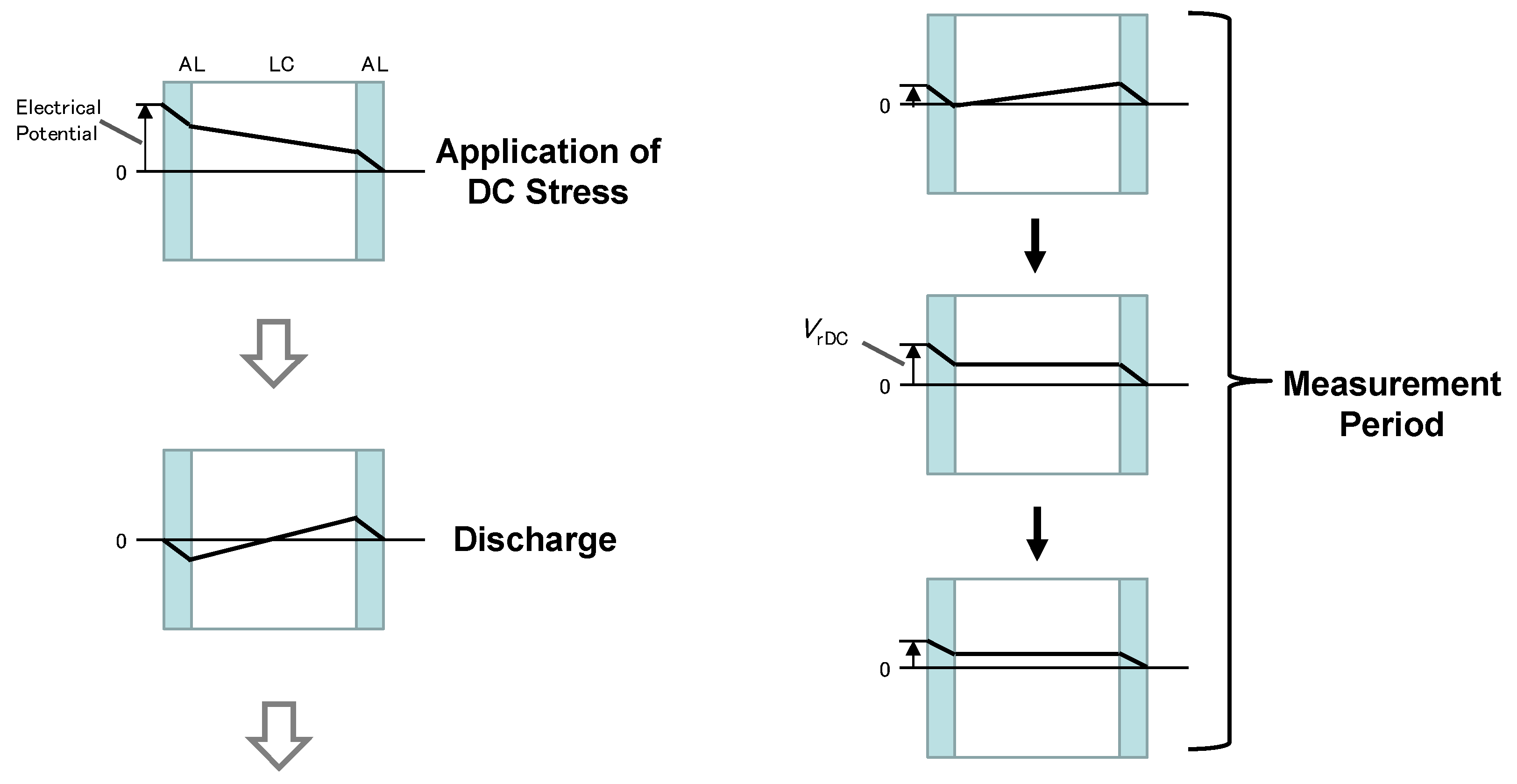
:1. Introduction
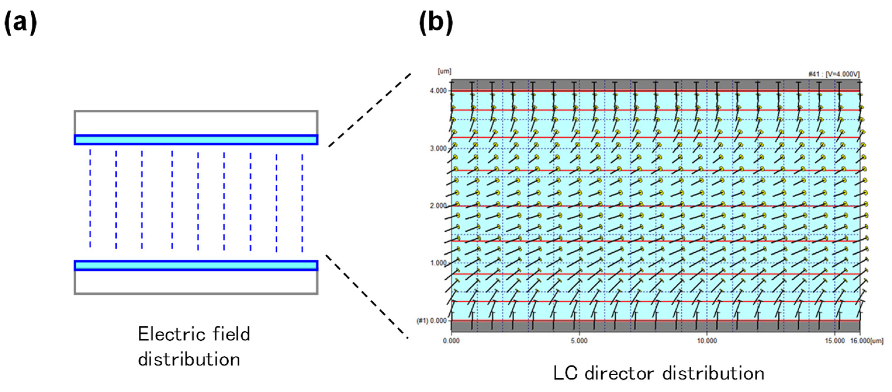
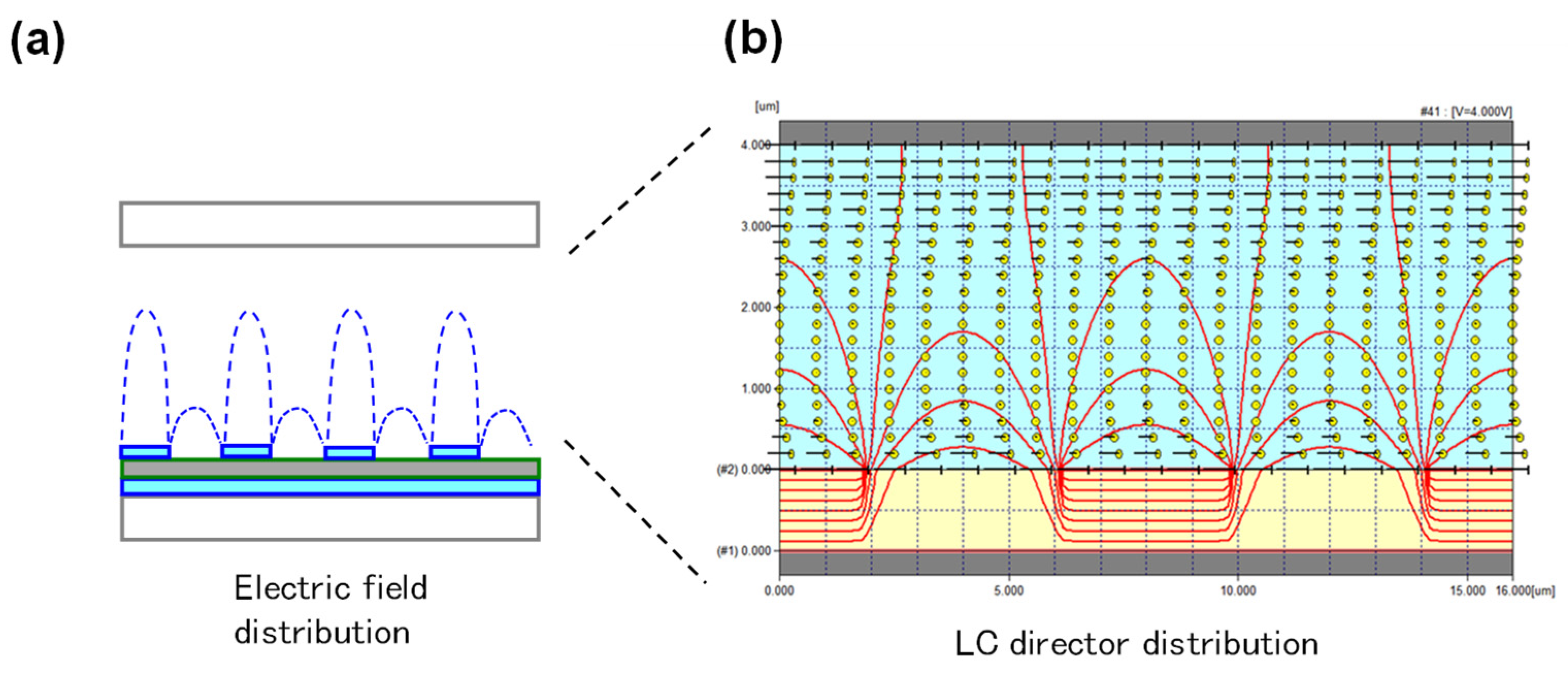
2. Two Types of the LC Cells
3. Preparation of LC Cells
4. Measurement of VA-LC Cell
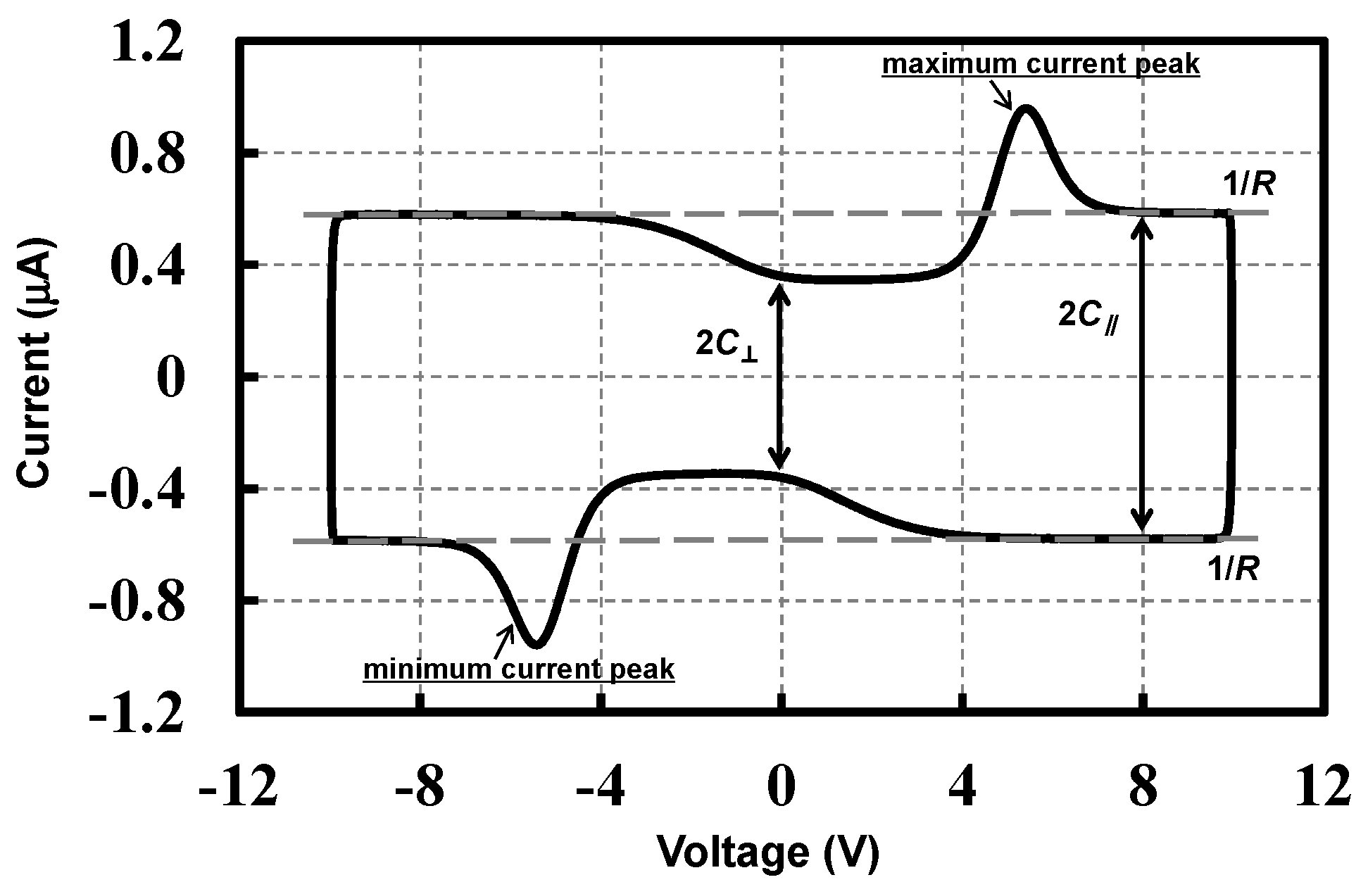
4.1. I-V Curve
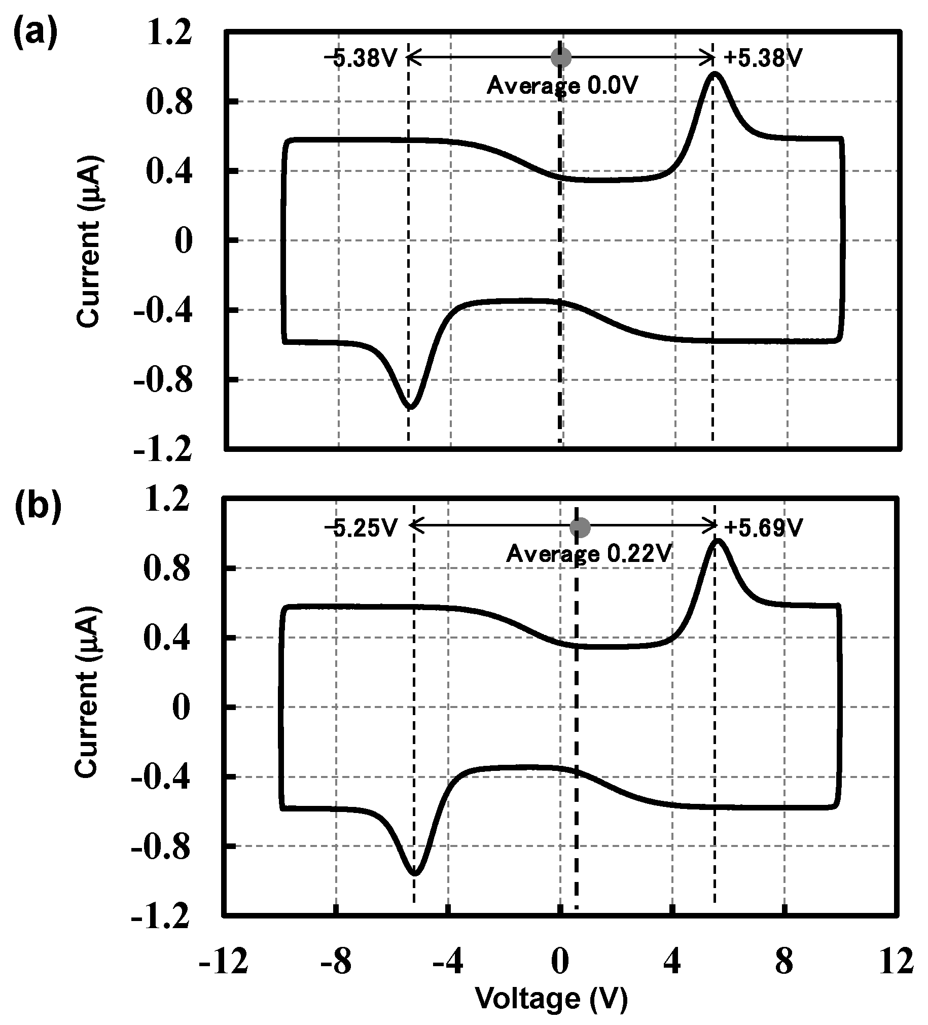
4.2. Determination of VrDC
4.3. Comparison of VrDC Determined by I-V Curve and Flicker Minimization
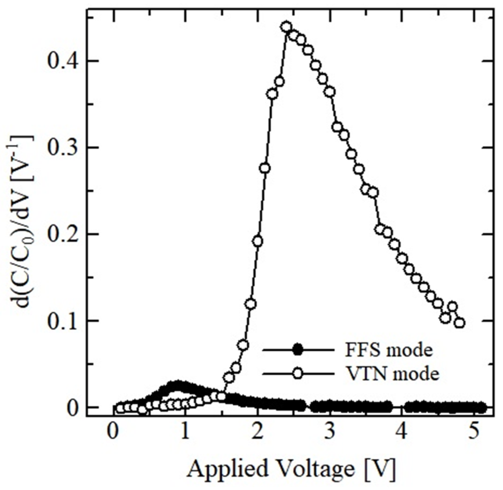
5. Measurement of FFS-LC Cell
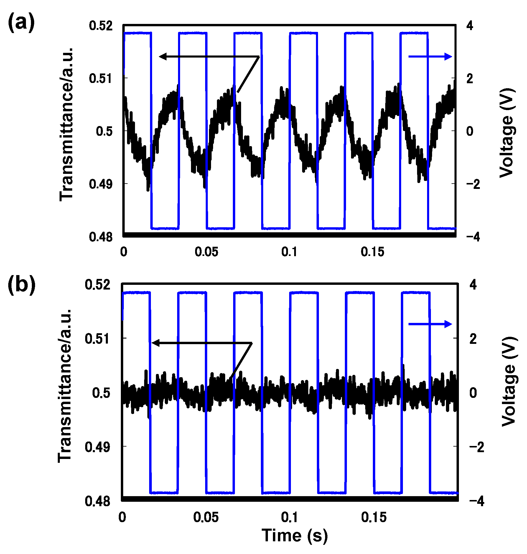
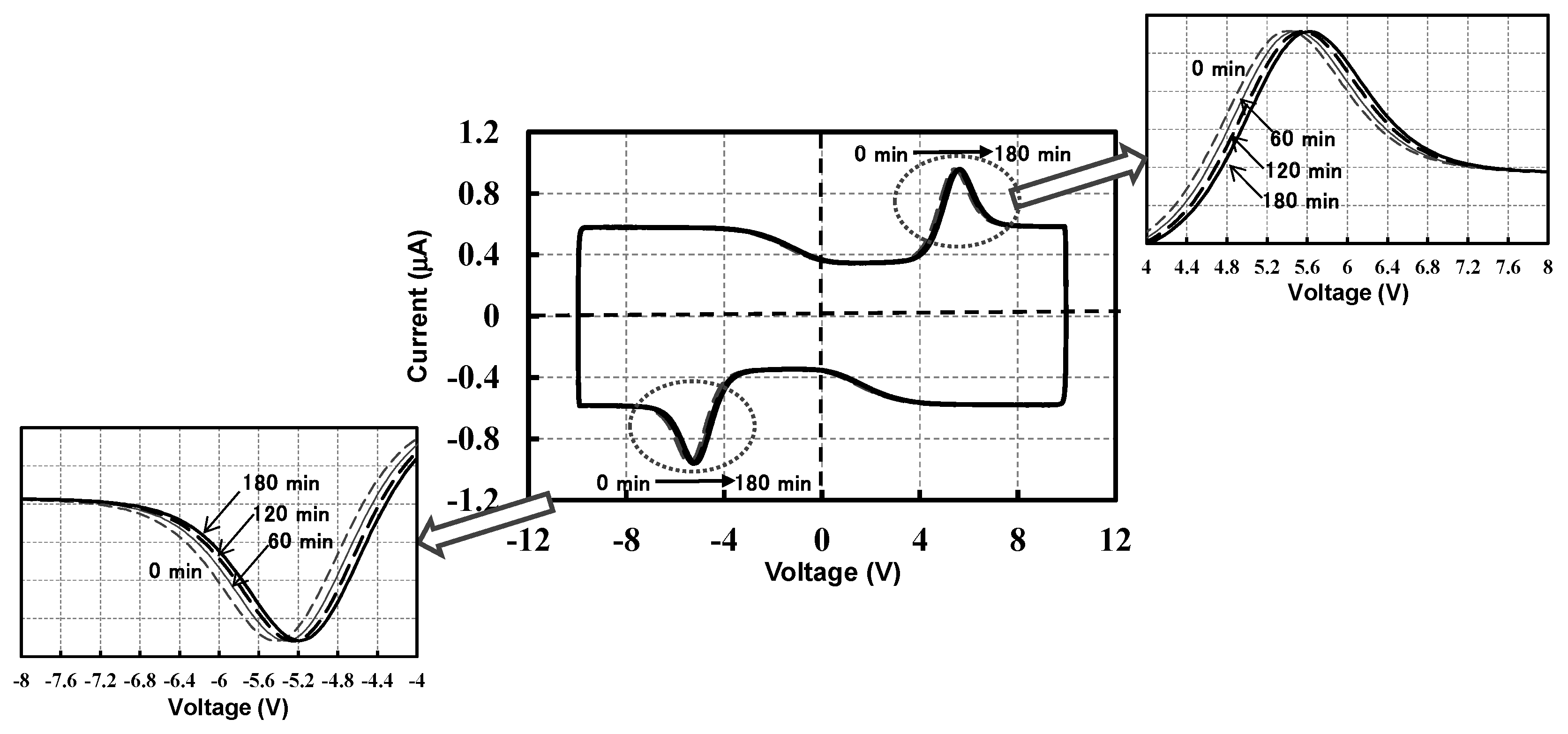
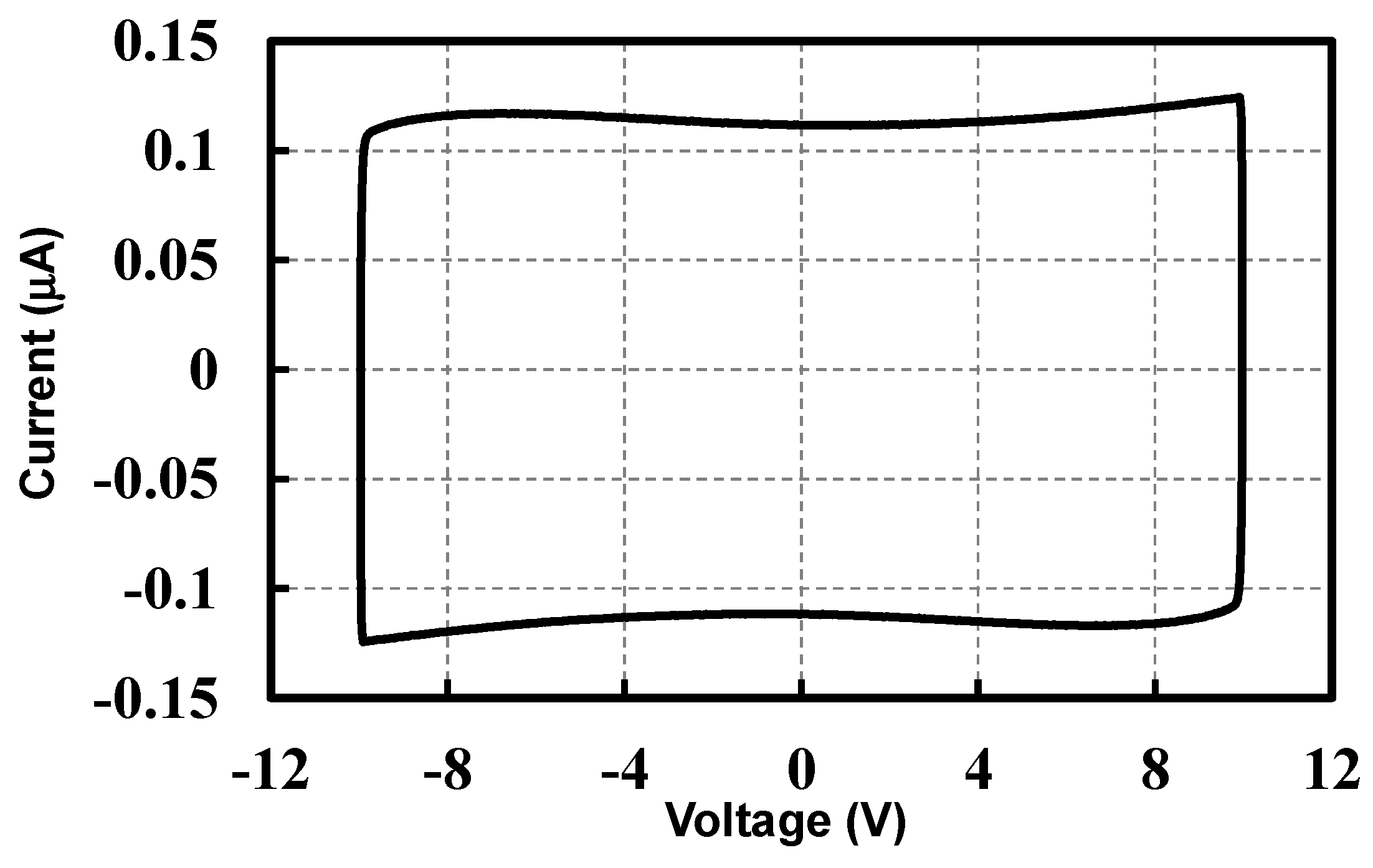
5.1. I-V Curve
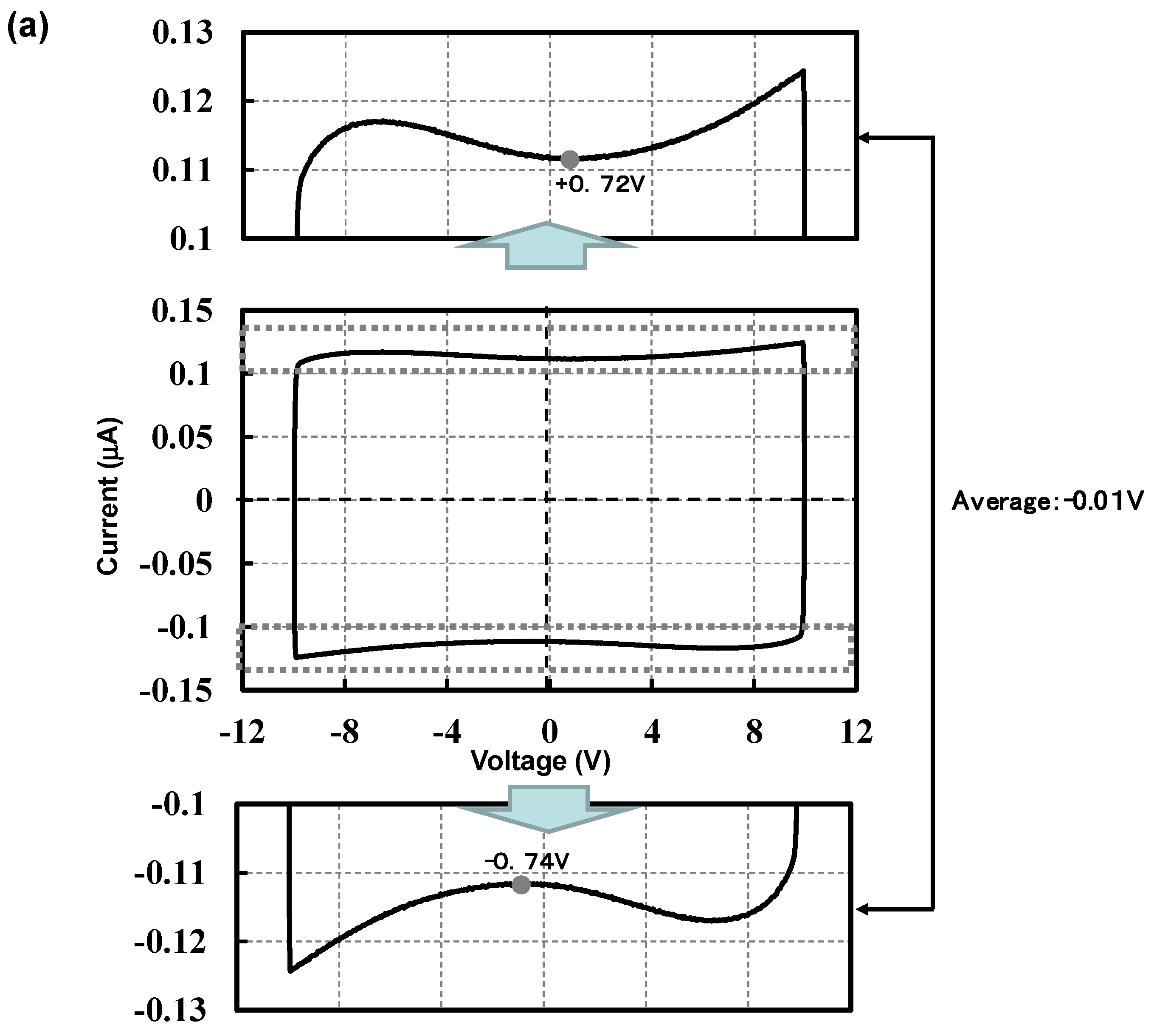
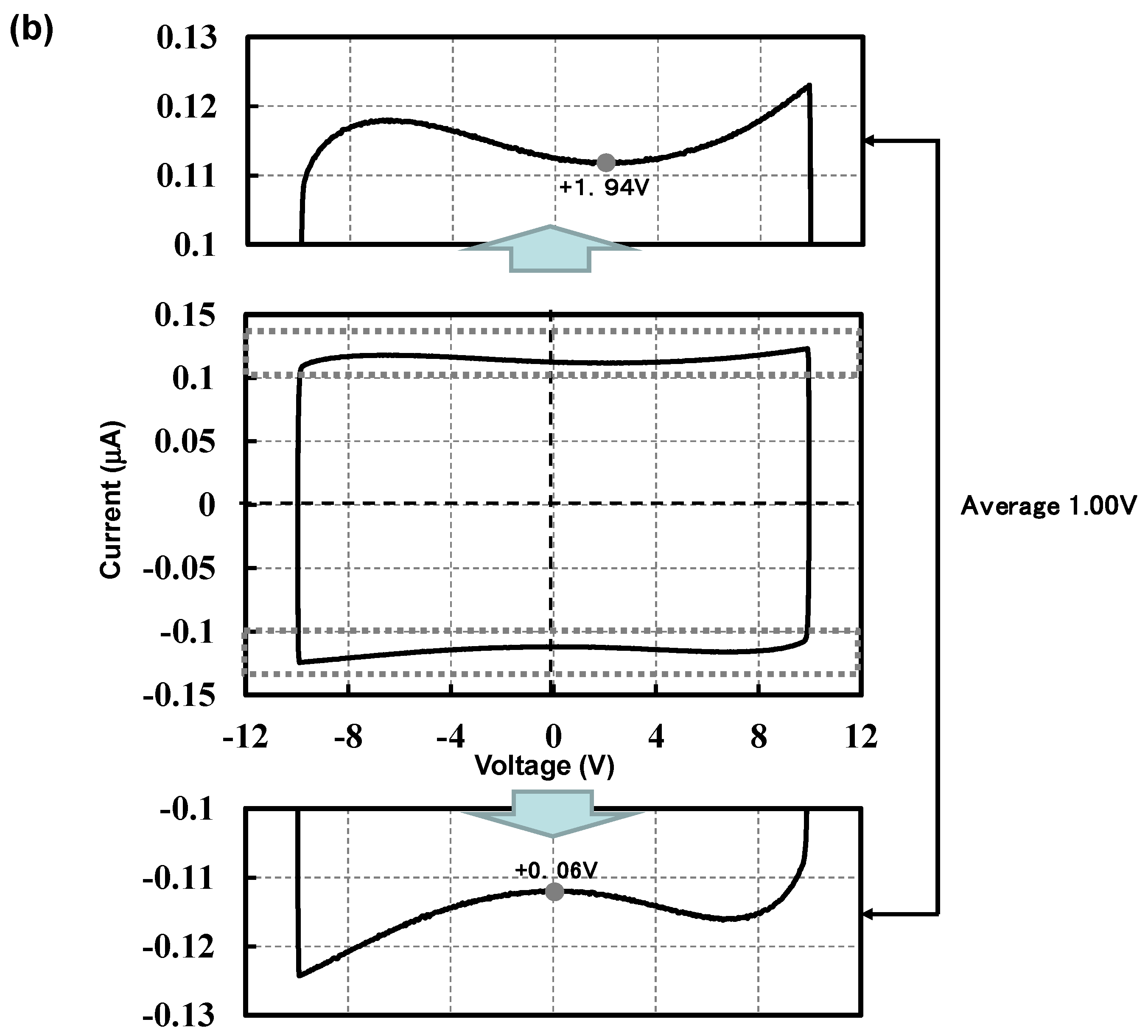
5.2. Determination of VrDC
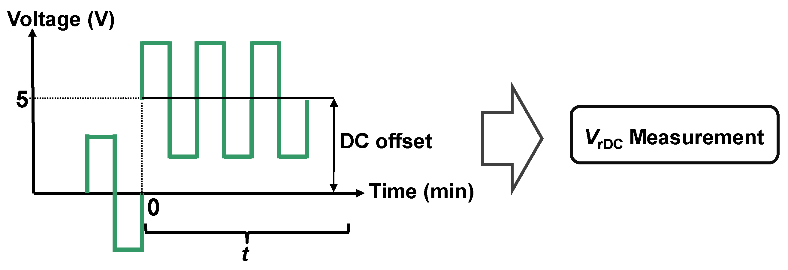
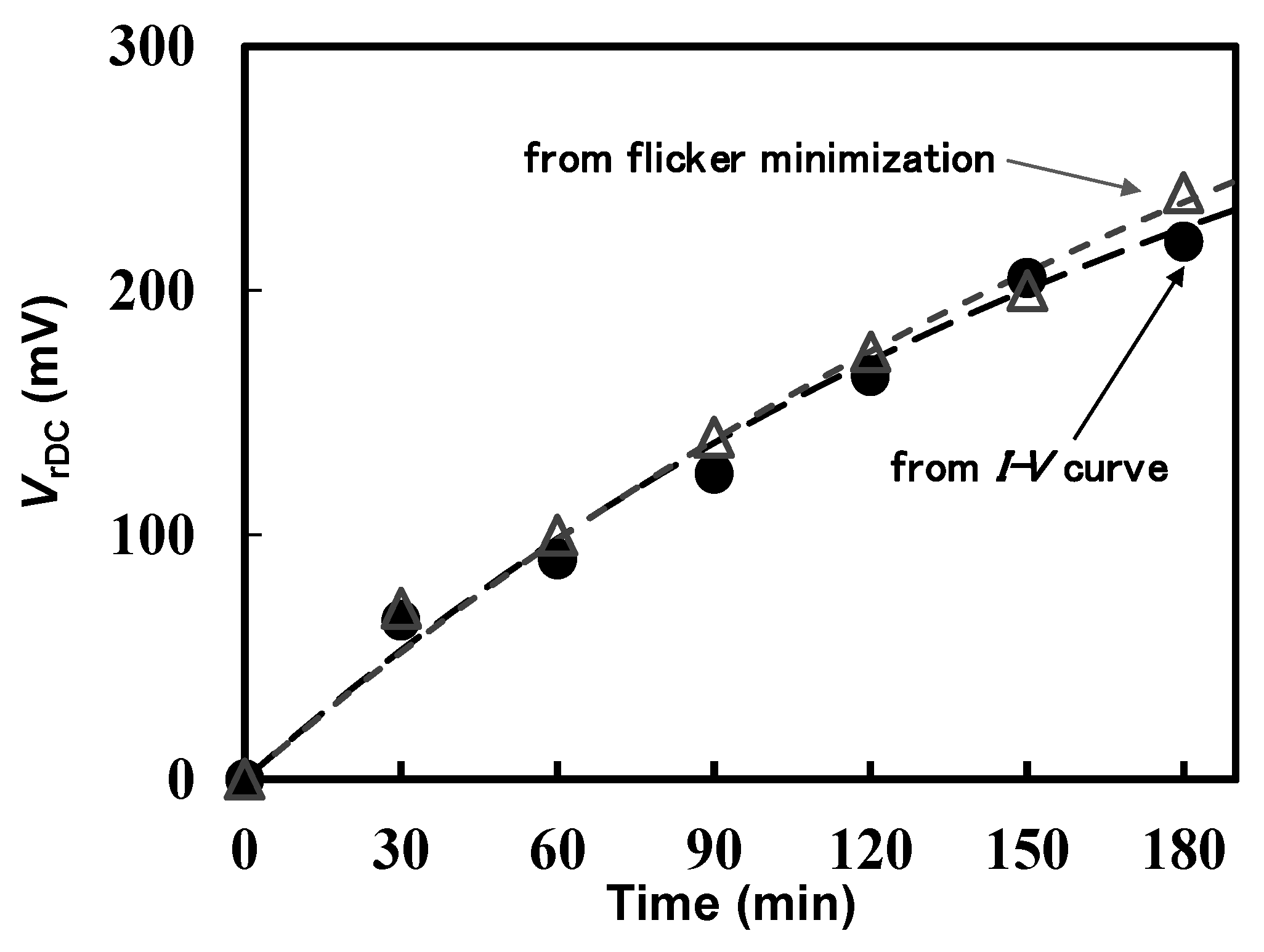
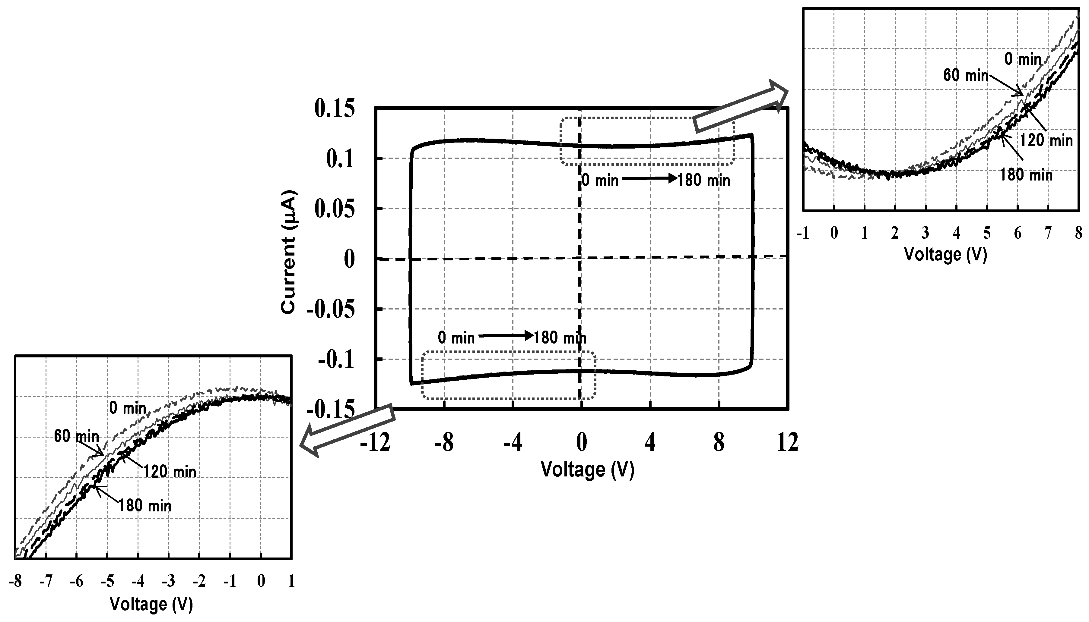
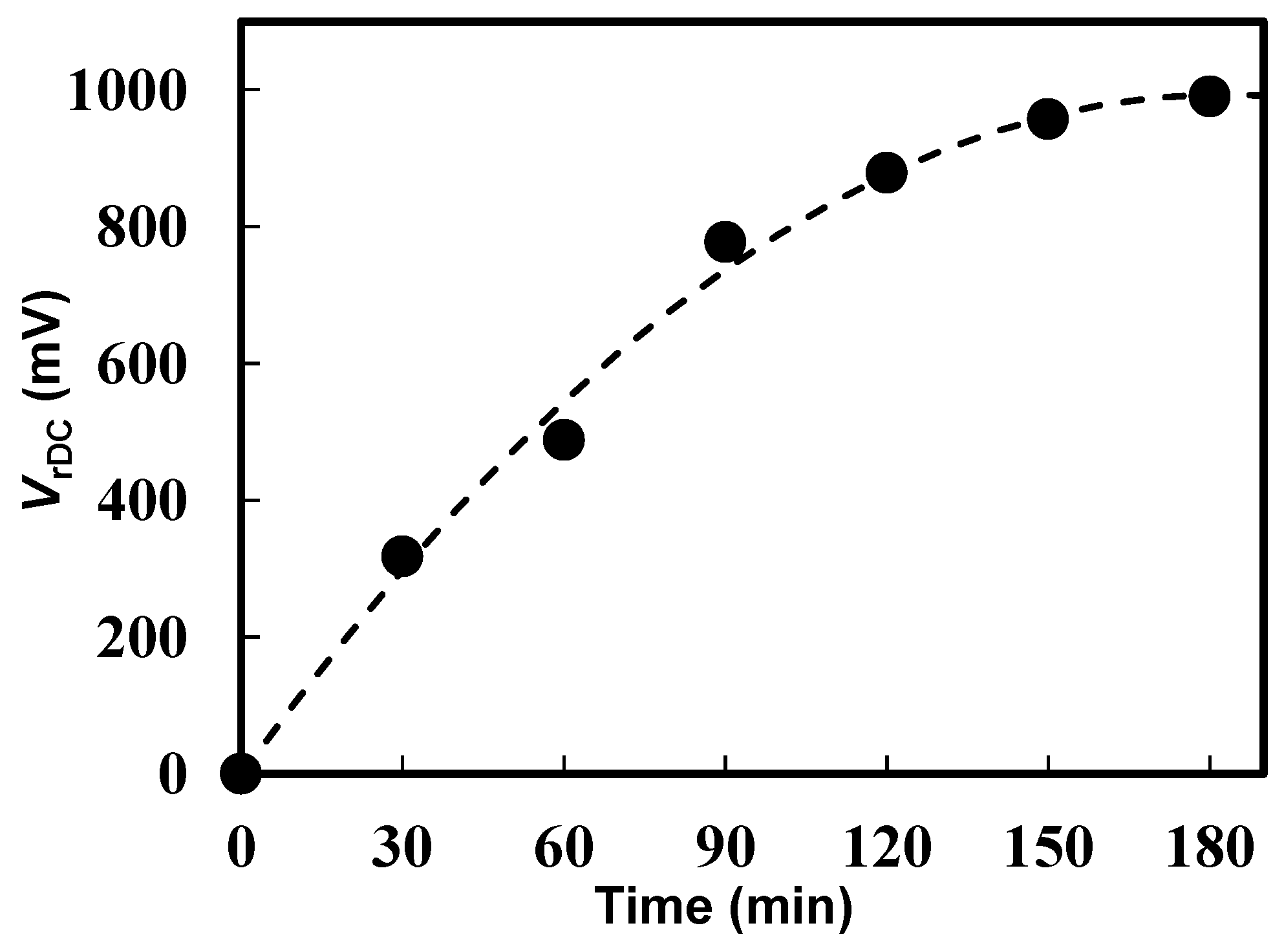
5.3. VrDC as a Function of Stress Time Measured by I-V Curve
6. Characteristics of the I-V Curve Shift Technique by the Triangular Voltage Application for Determination of the VrDC
7. Conclusions
Author Contributions
Funding
Institutional Review Board Statement
Informed Consent Statement
Data Availability Statement
Conflicts of Interest
References
- Ishihara, S.; Mizusaki, M. Alignment control technology of liquid crystal molecules. J. Soc. Inf. Disp. 2020, 28, 44–74. [Google Scholar] [CrossRef]
- Schadt, M. Nematic liquid crystals and twisted-nematic LCDs. Liq. Cryst. 2015, 42, 646–652. [Google Scholar] [CrossRef]
- Takeda, A.; Kataoka, S.; Sasaki, T.; Chida, H.; Tsuda, H.; Ohmuro, K.; Koike, Y.; Sasabayashi, T.; Okamoto, K. A super-high image-quality multi-domain vertical alignment LCD by new rubbing-less technology. SID Int. Symp. Dig. Tech. Pap. 1998, 29, 1077–1079. [Google Scholar] [CrossRef]
- Oh-e, M.; Kondo, K. Electro-optical characteristics and switching behavior of the in-plane switching mode. Appl. Phys. Lett. 1995, 67, 3895–3897. [Google Scholar] [CrossRef]
- Lee, S.H.; Lee, S.L.; Kim, H.Y. Electro-optic characteristics and switching principle of a nematic liquid crystal cell controlled by fringe-field switching. Appl. Phys. Lett. 1998, 73, 2881–2883. [Google Scholar] [CrossRef]
- Naemura, S. Liquid-crystal-material technologies for advanced display applications. J. Soc. Inf. Disp. 2000, 8, 5–9. [Google Scholar] [CrossRef]
- Huang, K.T.; Chao, A.; Yu, C.H. Image sticking analysis of different Q-time LC cell by machine vision. SID Int. Symp. Dig. Tech. Pap. 2007, 38, 665–668. [Google Scholar] [CrossRef]
- You, J.; Jung, J.; Choi, N.; Rhie, K.; Shin, S. The study of the correlation between surface anchoring energy and activation energy on patterned vertical alignment (PVA) mode. SID Int. Symp. Dig. Tech. Pap. 2007, 38, 673–676. [Google Scholar] [CrossRef]
- Chen, Y.-C.; Liu, P.-M.; Liao, C.-H.; Ting, T.-L.; Chang, T.-J.; Liao, W.-L.; Lien, A. Releasing behavior of image sticking. SID Int. Symp. Dig. Tech. Pap. 2008, 39, 1798–1800. [Google Scholar] [CrossRef]
- Kamoto, R. Analysis of image sticking on a real MVA cell. J. Soc. Inf. Disp. 2008, 16, 451–456. [Google Scholar] [CrossRef]
- Park, Y.; Kim, S.; Lee, E. A study on reducing image-sticking artifacts in wide-screen TFT-LCD monitors. J. Soc. Inf. Disp. 2007, 15, 969–973. [Google Scholar] [CrossRef]
- Seiberle, H.; Schadt, M. Influence of charge carriers and display parameters on the performance of passively and actively addressed LCDs. SID Int. Symp. Dig. Tech. Pap. 1992, 23, 25–28. [Google Scholar]
- Tanaka, Y.; Goto, Y.; Iimura, Y. Mechanism of DC offset voltage generation in hybrid-aligned nematic liquid crystal displays. Jpn. J. Appl. Phys. 1999, 38 Pt 2, L1115–L1117. [Google Scholar] [CrossRef]
- Mizusaki, M.; Miyashita, T.; Uchida, T.; Yamada, Y.; Ishii, Y.; Mizushima, S. Generation mechanism of residual direct current voltage in a liquid crystal display and its evaluation parameters related to liquid crystal and alignment layer materials. J. Appl. Phys. 2007, 102, 014904. [Google Scholar] [CrossRef]
- Mizusaki, M.; Miyashita, T.; Uchida, T. Behavior of ion affecting image sticking on liquid crystal displays under application of direct current voltage. J. Appl. Phys. 2010, 108, 104903. [Google Scholar] [CrossRef]
- Mizusaki, M.; Miyashita, T.; Uchida, T. Kinetic analysis of image sticking with adsorption and desorption of ions to a surface of an alignment layer. J. Appl. Phys. 2012, 112, 044510. [Google Scholar] [CrossRef]
- Xu, D.; Peng, F.; Chen, H.; Yuan, J.; Wu, S.-T.; Li, M.-C.; Lee, S.-L.; Tsai, W.-C. Image sticking in liquid crystal displays with lateral electric field. J. Appl. Phys. 2014, 116, 193102. [Google Scholar] [CrossRef] [Green Version]
- Inoue, M. Review of various measurement methodologies of migration ion influence on LCD image quality and new measurement proposal beyond LCD materials. J. Soc. Inf. Disp. 2020, 28, 92–110. [Google Scholar] [CrossRef]
- Nishikawa, M.; Suganuma, T.; Tsuda, Y.; Bessho, N.; Iimura, Y.; Kobayashi, S. Properties of voltage holding ratios of liquid crystal cells using organic-solvent-soluble polyimide alignment films. Jpn. J. Appl. Phys. 1994, 33 Pt 2, L1113–L1116. [Google Scholar] [CrossRef]
- Mada, H.; Suzuki, H. Reverse hysteresis loop of nematic liquid crystals in C-V characteristic due to static electric field. Jpn. J. Appl. Phys. 1987, 26, L1092–L1094. [Google Scholar] [CrossRef]
- Takahashi, S. The investigation of a dc induced transient optical 30-Hz element in twisted nematic liquid-crystal displays. J. Appl. Phys. 1991, 70, 5346–5350. [Google Scholar] [CrossRef]
- Huang, K.-T.; Huang, Y.-W.; Fang, R.-W.; Chao, Y.-T.; Lee, C.; Lin, S.-C.; Yu, C.-H.; Kao, C.; Jen, T.-S. A turning method to minimizing flicker shift phenomenon in positive FFS mode LCD panel and improve DC image sticking. SID Int. Symp. Dig. Tech. Pap. 2018, 49, 1711–1714. [Google Scholar] [CrossRef]
- Tsuruma, T.; Goto, Y.; Higashi, A.; Watanabe, M.; Yamaguchi, H.; Tomooka, T.; Kikkawa, H. Novel image sticking model in the fringe field switching mode based on the flexoelectric effect. In 31st International Display Research Conference 2011 (EuroDisplay 2011), Arcachon, France, 19–22 September 2011; Curran Associates, Inc.: Red Hook, NY, USA, 2011; pp. 15–18. [Google Scholar]
- Hatsumi, R.; Fukai, S.; Kubota, Y.; Yamashita, A.; Jikumaru, M.; Baba, H.; Moriya, K.; Kubota, D.; Kusunoki, K.; Hirakata, Y.; et al. FFS-mode OS-LCD for reducing eye strain. J. Soc. Inf. Disp. 2013, 21, 442–450. [Google Scholar] [CrossRef]
- Jeong, I.H.; Jang, I.W.; Kim, D.H.; Han, J.S.; Kumar, B.V.; Lee, S.H.; Ahn, S.H.; Cho, S.H.; Yi, C. Investigation on flexoelectric effect in the fringe field switching mode. SID Int. Symp. Dig. Tech. Pap. 2013, 44, 1368–1371. [Google Scholar] [CrossRef]
- Lee, D.-J.; Shim, G.-Y.; Choi, J.-C.; Park, J.-S.; Lee, J.-H.; Baek, J.-H.; Choi, H.C.; Ha, Y.M.; Ranjkesh, A.; Kim, H.-R. Transient flickering behavior in fringe-field switching liquid crystal mode analyzed by positional asymmetric flexoelectric dynamics. Opt. Express 2015, 23, 34055–34070. [Google Scholar] [CrossRef] [PubMed]
- Kim, M.S.; Bos, P.J.; Kim, D.-W.; Yang, D.-K.; Lee, J.H.; Lee, S.H. Flexoelectric effect in an in-plane switching (IPS) liquid crystal cell for low-power consumption display devices. Sci. Rep. 2016, 6, 35254. [Google Scholar] [CrossRef]
- Lee, S.H.; Lee, S.M.; Kim, H.Y.; Kim, J.M.; Hong, S.H.; Jeong, Y.H.; Park, C.H.; Choi, Y.J.; Lee, J.Y.; Koh, J.W.; et al. 18.1” ultra-FFS TFT-LCD with super image quality and fast response time. SID Int. Symp. Dig. Tech. Pap. 2001, 32, 484–487. [Google Scholar] [CrossRef]
- Miyachi, K.; Kobayashi, K.; Yamada, Y.; Mizushima, S. The world’s first photo alignment LCD technology applied to generation ten factory. SID Int. Symp. Dig. Tech. Pap. 2010, 41, 579–582. [Google Scholar] [CrossRef]
- Terashita, S.; Watanabe, K.; Shimoshikiryoh, F. Novel liquid crystal display mode “UV2AII” with photo alignment technology for a large-screen 8K display. SID Int. Symp. Dig. Tech. Pap. 2019, 50, 62–65. [Google Scholar] [CrossRef]


| C-V Hysteresis [19,20] | Flicker Minimization [16,21] | Dielectric Absorption [18] (Refer to Figure 1) | |
|---|---|---|---|
| Measuring method | Electrical | Optical | Electrical |
| Measurement item | Shift of C-V curve | Offset voltage to minimize optical flicker | Change of electrical potential |
| Correlation with the image sticking | High | High | Middle |
| Convenience for measurement | Easy | Difficult | Easy |
| Adaptivity to the LC cells with vertical electric field (TN, ECB, VA, VTN modes) | Applicable | Applicable | Applicable |
| Adaptivity to the LC cells with in-plane electric field (IPS and FFS modes) | No Data | Difficult | Applicable |
| Nega-LC | |
|---|---|
| TNI (°C) | 90 |
| ε∥ | 3.6 |
| ε⊥ | 7.8 |
| Δε | −4.2 |
| Δn | 0.083 |
| ρ (Ωcm) | 1.8 × 10¹³ |
| VTN-LC Cell | FFS-LC Cell | |
|---|---|---|
| d (μm) | 4.0 | 4.0 |
| C * 2 (nF) * 2 /25 °C | 1.3 | 0.28 |
| R (GΩ) * 3 /25 °C | 0.76 | 3.68 |
| VHR/70 °C | 98.4 | 98.1 |
| I-V Curve Shift | |
|---|---|
| Measuring method | Electrical |
| Measurement item | Shift of current maximum and/or minimum peaks |
| Correlation with the image sticking | High |
| Convenience for measurement | Convenient and easy |
| Advantage compared with the other techniques | Could be evaluated for both the LC cells with vertically- and in-plane electric fields |
Publisher’s Note: MDPI stays neutral with regard to jurisdictional claims in published maps and institutional affiliations. |
© 2021 by the authors. Licensee MDPI, Basel, Switzerland. This article is an open access article distributed under the terms and conditions of the Creative Commons Attribution (CC BY) license (https://creativecommons.org/licenses/by/4.0/).
Share and Cite
Mizusaki, M.; Ishihara, S. A Novel Technique for Determination of Residual Direct-Current Voltage of Liquid Crystal Cells with Vertical and In-Plane Electric Fields. Symmetry 2021, 13, 816. https://0-doi-org.brum.beds.ac.uk/10.3390/sym13050816
Mizusaki M, Ishihara S. A Novel Technique for Determination of Residual Direct-Current Voltage of Liquid Crystal Cells with Vertical and In-Plane Electric Fields. Symmetry. 2021; 13(5):816. https://0-doi-org.brum.beds.ac.uk/10.3390/sym13050816
Chicago/Turabian StyleMizusaki, Msanobu, and Shoichi Ishihara. 2021. "A Novel Technique for Determination of Residual Direct-Current Voltage of Liquid Crystal Cells with Vertical and In-Plane Electric Fields" Symmetry 13, no. 5: 816. https://0-doi-org.brum.beds.ac.uk/10.3390/sym13050816