1. Introduction
The GaN/InGaN material system has been widely employed for production of light emitting diodes (LEDs) and laser diodes (LDs), enabling many technologies from general illumination, to display, to high-speed communications [
1]. Despite the heavy development of these devices in the blue emission regime which has led to extremely high-efficiency devices, emission at longer wavelengths such as green, yellow, amber, and red typically experiences much lower quantum efficiencies, worsening with longer wavelengths [
2]. Indium incorporation in the active regions of these devices at high alloy contents, such as above x = 25% for In
Ga
N, becomes difficult to achieve without leading to significant microstructural degradation [
3,
4,
5]. This degradation worsens with increasing In content due to multiple factors, specifically the significant difference in sublimation temperature of In and Ga requiring lower growth temperatures, and the increasing lattice mismatch between the underlying GaN layer and the high-In content active regions [
6]. In turn, the poor structural quality of these high-In layers hinders the development of efficient long-wavelength emitting devices [
7,
8].
The compressive stress in the InGaN layer is due to the large lattice constant mismatch between the thick GaN buffer and the high-In layer, both increasing as In content increases [
9]. Substrates employing a relaxed InGaN layer to achieve a larger lattice constant can be used to reduce these lattice mismatch stresses. In this work, we employ relaxed InGaN substrates with an enlarged lattice constant to grow high-In epilayers. The enlarged lattice constant employed by these relaxed InGaN substrates compared to GaN leads to a reduction in compressive stress during growth in the as-grown layers, most significantly the active region quantum wells (QWs) [
10]. The compositional pulling effect also plays a role in these layers, where the incorporation efficiency of In decreases as strain becomes larger due to increasing lattice mismatch and resulting deformation energy of alloying the In atoms [
11,
12,
13]. As a result, mitigation of the compositional pulling effect through strain reduction in the high-In layer directly leads to an improvement in In incorporation efficiency [
14]. Additionally, the reduction in strain resulting from use of a relaxed InGaN substrate can also yield improved crystal quality in the QW through strain-generated defect reduction, resulting in higher PL efficiency than conventional GaN-on-sapphire growth [
15,
16].
One drawback to the use of relaxed InGaN substrates is the poor crystal quality and rough morphology of the substrate InGaN layer that must be recovered with further growth. Specifically, the substrates used in this work contain a native V-defect density of 5 × 10
cm
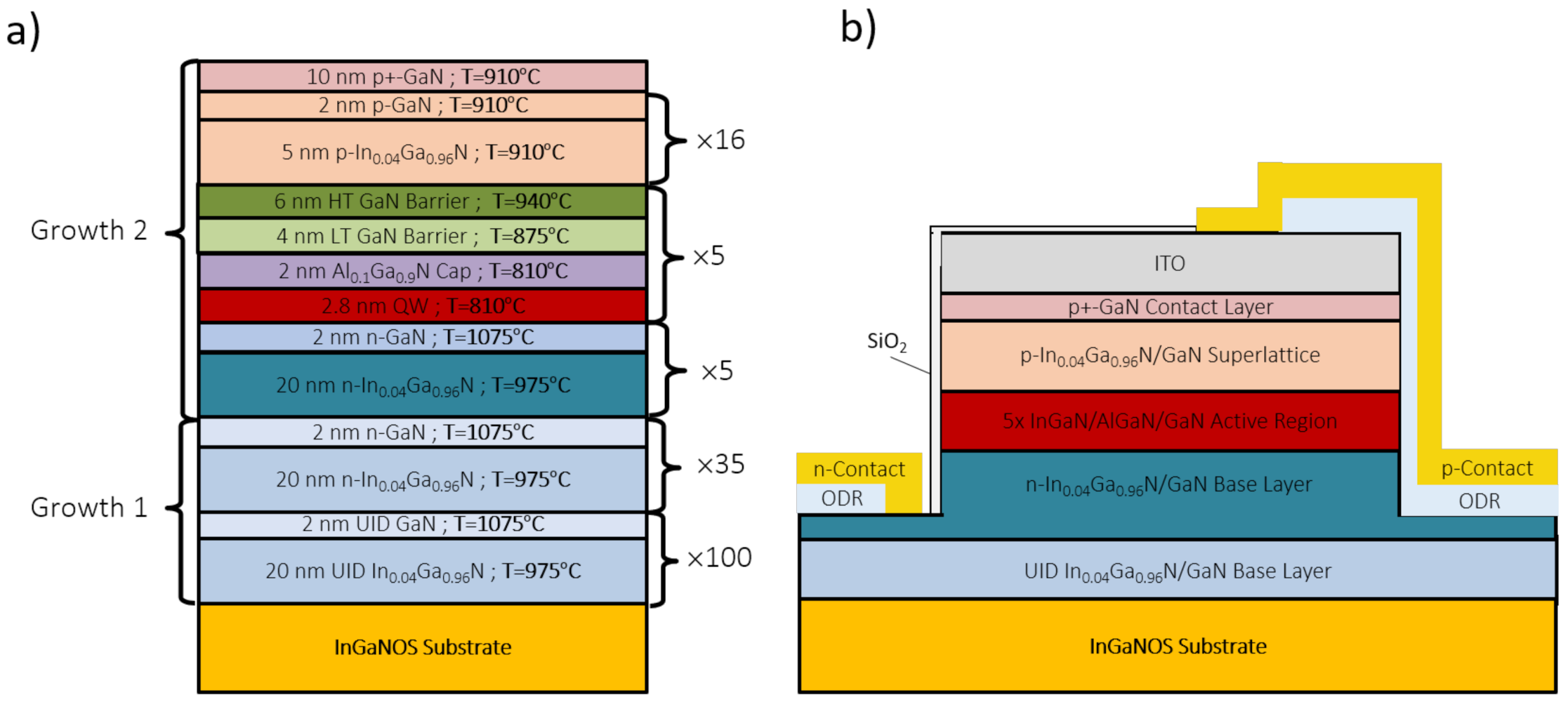
, but generally the substrate defect density will be dependent on the starting InGaN material. Additionally, further growth must take strain management into account with respect to the increased lattice constant, as a pure GaN layer would undergo tensile stress under this growth condition and eventually crack with sufficient thickness. In our previous work, we developed a base layer scheme consisting of a InGaN/GaN buffer/interlayer structure designed to fully eliminate the V-defects and achieve high crystal quality. These base layers employ optimized growth conditions for buffer and interlayer thicknesses, temperatures, V/III ratio, and carrier gasses [
17]. This base layer was also designed to match the lattice constant of the substrate, maintaining the relaxed strain state present initially. With a base layer free from V-defects and with good morphology, the advantages of the relaxed InGaN substrate and increased lattice constant can be used in the realization of
LED devices [
18]. Importantly, the reduction of the compositional pulling effect resulting from the reduction in strain during growth can then be applied to QW growth, allowing for higher temperatures to be used while still achieving high In content in a red-emitting device.
In this work, we demonstrate high-performance LEDs with red emission using an InGaN base layer with thin GaN interlayers and optimized p-type InGaN/GaN superlattice structure grown on relaxed InGaN substrates, leading to improved light output power and external quantum efficiency (EQE). Fabricated devices are analyzed in terms of their emission spectra, current density-voltage (JV) behavior, and their packaged device EQE results to determine improvements in light output power and efficiency, assuming a light extraction efficiency (LEE) of approximately 30% for a rudimentary surface-mounted and encapsulated package. Finally, atomic probe tomography (APT) is employed to measure the In content of the QW region, yielding some insight into the magnitude of the reduction of the compositional pulling effect and its effect on In incorporation. Compared to previous published devices, we realize 609 nm red electroluminescence with a significant increase to the light output power, achieving working LED devices with an EQE approaching 1% at this long wavelength.
2. Methods
Substrates used throughout this study are provided by SOITEC, a private company, and are referred to hereafter as “InGaNOS” substrates. The substrates are composed of 490 × 490
m
InGaN mesas spaced by 10 μm gaps between them forming a grid on top of a buried oxide layer and sapphire substrate. The lattice constant and amount of substrate relaxation can be altered based on the defined substrate mesa size and In content. This technology enables partially relaxed InGaN patterns from 490 × 490
m
down to few
m
and large lattice parameters up to 3.219 Å. The substrate mesas are 150 nm thick and have a nominal lattice constant of 3.205 Å for all samples examined here, with a buried oxide (BOX) underneath between the sapphire and mesas. These substrate templates employ a nominal In content of 4% with 54% relaxation, and the relaxation can be tuned using SOITEC’s proprietary Smart-Cut technology. Structurally, the epi-ready InGaNOS substrates contain a native V-defect density of around 5 × 10
cm
, and an X-ray rocking curve FWHM of 2600 arcsec for the (0002) reflection. More specific details on substrate processing and fabrication, as well as fundamental structural and optical quality characterization can be found in ref. [
14].
Samples were grown by atmospheric pressure MOCVD on InGaNOS substrates employing triethylgallium (TEGa), trimethylaluminum (TMAl) trimethylindium (TMIn), and ammonia (NH
) as the precursors for GaN, AlGaN, and InGaN growth. For n- and p-type dopants, disilane (Si
H
) and Bis(cyclopentadienyl) magnesium (Cp
Mg) were used as precursors, respectively. Nitrogen and hydrogen were both employed as carrier gasses. The Si doping concentration for the n-type InGaN/GaN:Si base layer was 5 × 10
cm
throughout the study. We also employed a Mg concentration of 8 × 10
cm
for the p-type doping in the InGaN/GaN:Mg region. Base layers were grown at a temperature of 975 °C for the InGaN regions and 1075 °C for the high temperature (HT) GaN interlayers. The doped portion of the InGaN/GaN base layer formed the n-contact layer for the subsequently grown device. For all samples, the HT GaN interlayers eliminate the pre-existing V-defects and prevent creation of new ones. The growth and characterization of the base layer, as well as study of the V-defect elimination mechanism, were thoroughly examined in previous work [
17]. Regrowth of the active region and p-type regions is performed on one of the batch-grown base layers. Active regions consist of 5 periods of 2.8 nm thick InGaN QWs, 2 nm AlGaN cap layers containing a 10% Al content, 4 nm lower temperature (LT) GaN quantum barriers (QBs), and 6 nm HT GaN QBs grown in sequence. Details on the active region structure can be found elsewhere [
19]. The p-type region under investigation here has a nominal thickness total of 110 nm and consist of an InGaN/GaN:Mg superlattice structure with periodicity of 5/2 nm grown entirely at 910 °C, capped by a 10 nm GaN:Mg p-contact layer with an increased doping of 1 × 10
cm
Mg for better ohmic contact. A schematic of the as-grown device can be seen in
Figure 1a for reference.
Atom probe tomography (APT) was performed to determine the In content of the QWs in these devices. Sample preparation was performed by coating the epi samples with 200 nm Ni metal, and a small section of the sample was removed using focused ion beam (FIB) with a FEI Helios Dualbeam Nanolab 650 to create an APT tip for analysis. APT measurements were then performed using an Imago LEAP 3000X HR Atom Probe Microscope.
For fabrication of devices from as-grown epi, we employed an identical
LED process for all samples. First, the samples were submerged in heated aqua regia and then a standard solvent clean was performed to remove any surface impurity contamination, remaining surface Mg, or other growth residues. After sample cleaning, 110 nm of indium tin oxide (ITO) was deposited as a transparent conducting oxide (TCO) layer using electron-beam deposition for use as a p-contact. Devices were then defined using reactive-ion etching (RIE), first with a methane/hydrogen/argon plasma to etch the ITO layer, then using SiCl
to as a self-aligned etch of the III-nitride epi down to the n-GaN layer. After etching, an omnidirectional reflector (ODR), consisting of three periods of silicon dioxide (SiO
) and tantalum oxide (Ta
O
) layers followed by an aluminum oxide Al
O
capping layer was deposited using ion beam deposition (IBD). The periodic SiO
and Ta
O
layers act as a sidewall reflector while the Al
O
layer acts as a contact sticking layer, allowing dielectric isolation and good contact adhesion. Next, atomic layer deposition (ALD) was used as a sidewall passivation, depositing 50 nm of SiO
at 300 °C in a blanket deposition. After ALD, selected areas of SiO
were removed using buffered hydrofluoric acid (BHF) for contact deposition. Common contact pads for the p- and n-side were composed of 500/100/500 nm of Al/Ni/Au and deposited using electron-beam deposition. A full schematic of the fabricated device structure can be seen in
Figure 1b. Further detail on the fabrication process for these microLED devices can be found in reference [
20].
Packaging of the processed on-chip devices was performed manually. Devices were singulated using a dicing saw and cleaned with standard solvents. Selected devices were then mounted to the surface of conductive silver headers with Dow Corning OE 6550 optical epoxy and baked to cure the mounting epoxy. Next, Au wire bonds were attached with a wire bonder. Optical epoxy was then added as a lens and encapsulating material and baked to cure, completing the device. From basic light extraction modelling, the light extraction efficiency (LEE) of the package is estimated to be approximately 30%. Absorption in the InGaNOS substrate will also further reduce the LEE of the complete packaged device. Electrical testing of the finished devices was performed using a Keithley source generator and light collection was performed using an Instrument Systems integrating sphere.
3. Results
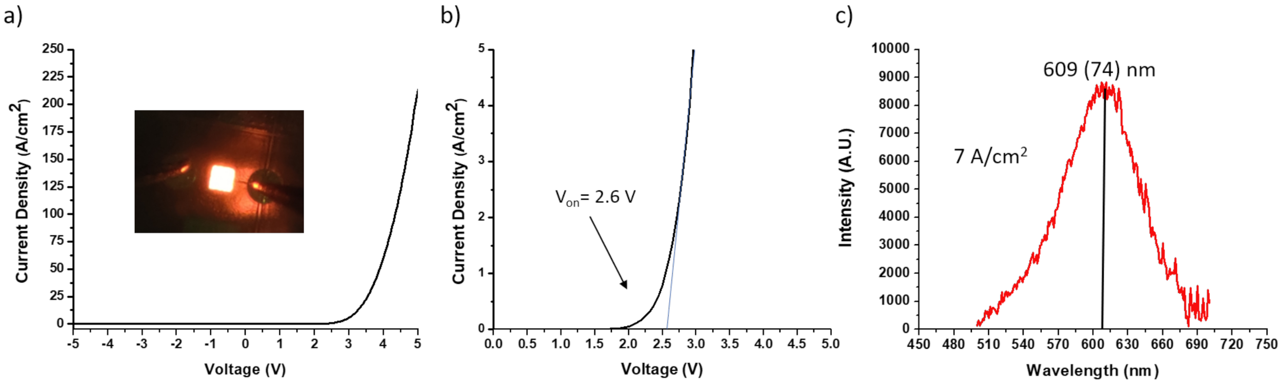
To characterize the performance of the fabricated
LED devices, we first examine the basic electrical behavior of a representative device and its emission characteristics. The current density-voltage response is seen in
Figure 2, along with a more specific look at the low current-density range near the turn-on region of the device. From
Figure 2a, typical diode-like behavior can be clearly visualized across a wide voltage range. An optical image of the device under operation at a moderate current density of 20 A/cm
can also be seen in the inset image in
Figure 2a. While the resistance of the LED may be somewhat high at a value of 2695
at 20 A/cm
corresponding to 3.45 V, significant current density is accessible in the examined bias range. Furthermore, extremely low leakage current density can be seen, with only 2.81 mA at −5 V bias. The turn-on voltage of the device (seen more clearly in
Figure 2b) is 2.6 V, determined from the regression of the linear region of the JV curve in the low-current-density regime shown in
Figure 2b. Finally, the EL emission spectra for the device is shown in
Figure 2c, indicating red emission at 609 nm at a current density injection of 7 A/cm
corresponding to 3.01 V. At this wavelength, the EL emission spectra has a FWHM of 74 nm and a single peak, relatively broad but a broadness typical of long-wavelength LEDs [
21]. This broad FWHM typically present in the red-emitting LEDs is a result of significant In fluctuation, which worsens as the In mole fraction in the QW increases [
22,
23,
24]. These parameters were reproducible throughout multiple operation cycles and after continuous high-current operation. Here, red emission is achievable and detectable even at low-current-density injection of 7 A/cm
near the LED turn-on and emits a clearly visible EL peak.
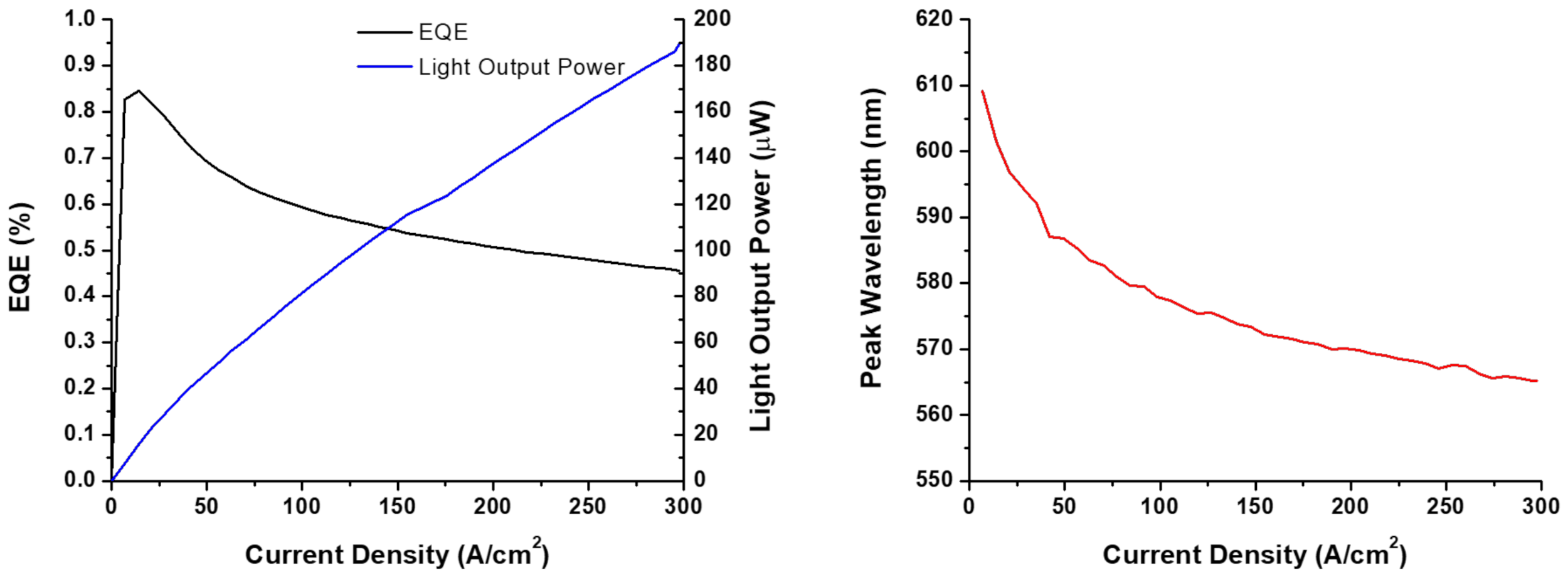
Selected on-chip devices were encapsulated into device packages to ascertain the power and efficiency of a finished, packaged device module in an integrating sphere. The light output power steadily increases with current density injection for a representative device, steadily becoming more sublinear (
Figure 3) with increasing current density. This lower power is due to both a small heating effect under continuous operation as well as the increasing effect of Auger recombination at increasing current density. Rather than a steady increase mimicking the shape of the power curve, the EQE curve takes on a “droop” shape typical of nitride LEDs. A peak EQE value is typically reached at low to moderate current densities, followed by a steady decline in EQE as current density is increased. The peak EQE of the device is 0.83%, occurring at a wavelength of 609 nm and a current density value of 7 A/cm
corresponding to 3.01 V. Despite the strain reduction benefits of the relaxed substrate with enlarged lattice constant, the remaining strain still present in the QW results in unresolved piezoelectric fields, leading to the QCSE, higher Auger recombination, and ultimately leading to EQE droop. However, red emission from a microLED device with EQE approaching 1% shows that the optimized growth methods for the device epilayers show improved device performance.
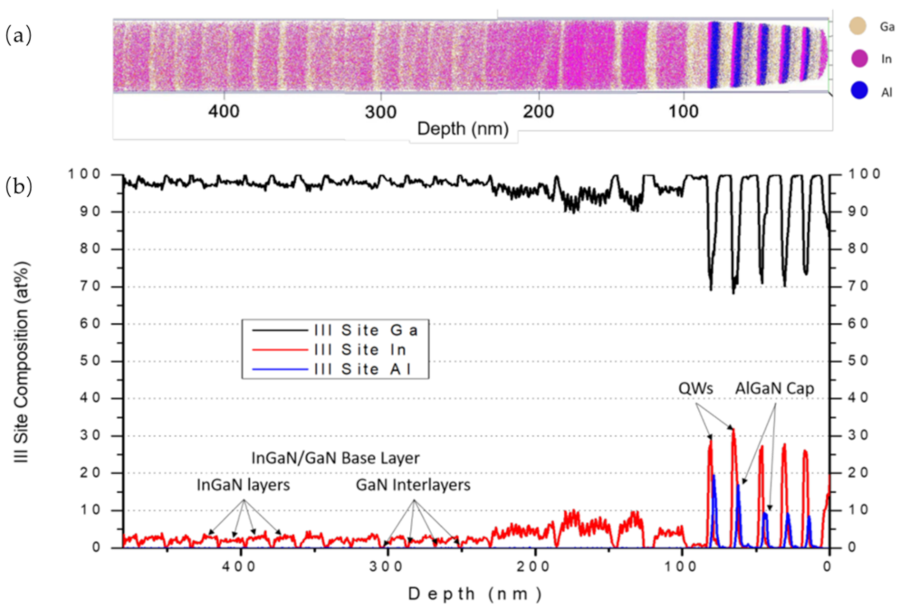
To further characterize the active region of these devices and confirm the true In content present when grown on relaxed substrates, APT was performed on the LED sample. The reconstruction of the APT tip sample is shown in
Figure 4a, where the active region can be seen as alternating layers of high-In InGaN QWs, AlGaN capping layers, and GaN quantum barriers (QBs). Furthermore, the lower buffer regions can be seen as with a defined layer structure of InGaN regions and thin GaN interlayers.
Figure 4b then further characterizes these regions, with the group-III content plotted for Ga, In, and Al corresponding to the sample reconstruction. Since the purpose of the GaN interlayer is to prevent the transition to a 3D growth mode by eliminating the surface riding In that increases as growth proceeds, some slight In nonuniformity in each individual InGaN layer can be seen surrounding these GaN interlayers. Both the quantitative atomic composition profile and spatial reconstruction are in agreement, especially visible in the nominally pure GaN regions, i.e., the thin interlayers in the base layer region below the QWs, and GaN quantum barriers. In the QWs, an In content of up to 32% can be seen even with the high QW growth temperature (810
C) used during growth. Despite each QW with nominally identical growth conditions, their In contents fluctuate slightly. However, the AlGaN capping layers unexpectedly have Al content of either approximately 10% or 20% despite also with identical growth conditions. Capping layers were expected to contain 10% Al, and the reason for the discrepancy in Al content of the capping layers of first two QWs is currently under investigation. It should also be noted that the two higher Al capping layers also reside above the two higher-In QWs, QW1 and QW2 at 28.8% and 32.0% In, respectively while QWs 3, 4, and 5 have a measured In content of 26.2%, 26.9%, and 26.3%, respectively, with 10% Al capping layers.
4. Discussion
The design of the epitaxial growth scheme (
Figure 1a) enables these high-efficiency red microLEDs using an optimized base layer to preserve material quality before growth of the active region, high temperatures during QW growth, and optimized p-type superlattice. The InGaN/GaN base layer design allows for elimination of V-defects prior to the active region, and significantly improves the crystal quality of the almost entire InGaN-based device despite the increased difficulty when growing an InGaN alloy [
17]. Additionally, this base layer design allows the benefit of the substrate’s enlarged lattice constant to be leveraged in the active region to reduce the compositional pulling effect, increasing the In incorporation efficiency as the effective strain at the growth interface decreases. As a result, of reducing the compositional pulling effect, the In incorporation during QW growth is significantly increased, enabling high In content up to 32% (
Figure 4) resulting in red emission from the QW. Additionally, the significantly improved In incorporation from strain management allows the use of increased temperatures during QW growth while achieving the same In content. In this case, 810 °C can be used to achieve an In content that results in red emission, much higher than typical QW growth temperatures used for conventionally grown red-emitting microLEDs [
25]. Notably, the 810 °C QW growth temperature used here for a red-emitting LED on InGaNOS is more typical of a green-emitting LED grown on conventional sapphire in the same reactor. Finally, the p-type design also employs an InGaN/GaN structure similar to that of the base layer, but in this case with thinner InGaN periods than previously fabricated LEDs for improved crystal quality due to less ternary alloy growth and higher power. With these aspects of epitaxial growth design all optimized, the overall growth scheme is tailored for high-In InGaN growth and superior device performance.
Devices fabricated from samples using this epitaxial design yield state of the art electrical and optical emission characteristics for red-emitting InGaN microLEDs grown on relaxed substrates. The turn-on voltage determined from the JV plot in
Figure 2a,b is quite low at a value of 2.6 V. This turn-on voltage is especially low considering the photon voltage of 2.03 eV for 609 nm emission, indicating little barrier to carrier transport. This is further supported by the low voltage, 3.45 V, present at an injection current density of 20 A/cm
. Even considering the relatively high dynamic resistance of the device under operation, the low turn-on and operational voltages indicate good charge transport to the QW even at a bias similar to the expected band gap energy. Additionally, the EL emission spectrum at 7 A/cm
shows a clear peak at 609 nm, a red-emitting device. At such long peak wavelengths, the FWHM of the emission spectra is also quite high at 74 nm. High FWHM is to be expected at long wavelengths, as the alloy fluctuation naturally present during the growth of InGaN becomes more extreme with increasing In content [
26,
27].
Most strikingly, devices yielded improved power and efficiency at long wavelengths. From integrating sphere measurements of optoelectrical device performance (
Figure 3), typical devices possess an EQE of 0.83%, higher than other reported red-emitting III-N devices beyond simple proof of concept devices [
28,
29]. Notably, this EQE value is achieved even with only basic packaging with unoptimized LEE. High EQE has been reported on some red devices employing relaxation via V-defects, [
7] but only with large-area devices grown on Si substrates rather than
LEDs on sapphire like those reported here. The high efficiency of the device while maintaining long-wavelength red emission represents a record performance for III-N devices grown on relaxed substrates. In short, the characteristic droop shape confirms the defect density of the device is sufficiently low, allowing a high enough carrier density to be achieved in the QW to display Auger-dominated recombination. Similarly, the power increases nearly linearly with current density injection, with some roll-off present in the droop regime. Examining the output across the same current density range, the emission wavelength becomes shorter with increasing current density, resulting in an expected “blueshift” to the emission due to screening of polarization-related electric fields. This example of blueshift yields 40 nm of peak wavelength shift over 300 A/cm
, with about 20 nm of shift between 0 and 50 A/cm
. Though this blueshift occurs throughout the measurement range examined, the small shift over the typical operation range (often targeted to be less than 10 A/cm
for
LEDs) indicates good control over the strain and resulting net electric field that causes carrier screening. Ultimately, the measured high-efficiency value, typical power and efficiency behavior, and well-managed characteristic blueshift indicate high-performance devices for red-emitting microLEDs.
Finally, the true sample structure can be seen in the APT reconstruction of the sample in
Figure 4a. The base layer InGaN/GaN scheme can be clearly viewed from this reconstruction, as can the active region structure, indicating good layer structure present throughout the growth. Benefits of the increased substrate lattice constant and resulting reduction in the compositional pulling effect can be directly seen through APT measurement and reconstruction, where the high-In content of the QW is confirmed. Despite the high growth temperature of the QW for red emission, an average QW In content of 28.1% was measured along with a maximum QW In content of 32.0%, consistent with the red emission. Unexpectedly, the Al content present in the capping layer of QW1 and QW2 is elevated to approximately 20% despite possessing the same growth conditions. Each QW in the active region possessed identical growth conditions, where the capping layers are calibrated to 10%. Interestingly, higher In contents were seen in the wells corresponding to the highest Al capping layers, suggesting that the capping layer may play an important role in further retention of In in the QW. We hypothesize that the higher Al content capping layer allows for increased thermal protection of the high-In QW during later high temperature growth of the QB and p-type region. With the QW better thermally protected, less In desorption occurs as a result of thermal degradation. Typically, the temperature used here during QW growth would result in much lower In content, more similar to the content of a green-emitting LED. Especially when considering the growth temperature, this APT measurement conclusively confirms the improved In incorporation in the QW through strain management from an increased lattice constant.


 ,
, 


