Article

A Novel Compensation Circuit for Capacitive Power Transfer System to Realize Desired Constant Current and Constant Voltage Output

1
State Grid Jiangsu Electric Power Co., Ltd., Guanyun County Power Supply Company, Lianyungang 222200, China
2
School of Electrical Engineering, Southeast University, Nanjing 210096, China
*
Author to whom correspondence should be addressed.
Submission received: 31 December 2021 / Revised: 7 February 2022 / Accepted: 17 February 2022 / Published: 18 February 2022

Abstract

:
Capacitive power transfer (CPT) technique possesses the advantages of safety, isolation, low cost, and insensitivity to conductive barriers. To charge lithium-ion batteries, CPT should possess the output profile consisting of first constant current (CC) output and later constant voltage (CV) output. To fulfill the output profile, many power switches or compensation components are added in the CPT circuit, which is not expected due to the bulky size and additional losses. To reduce the redundancy of the CPT system, an Lx-PS CPT circuit with only five compensation components is proposed in this paper. After a systematic analysis and a parameter design procedure, the proposed CPT circuit can realize input ZPA at both CC and CV modes. In addition, the output current at CC mode and the output voltage at CV mode are all adjustable based on the charging demands of different loads. Finally, simulations are done to prove the analysis in this paper. Compared to previous research, the CPT circuit proposed in this paper can not only achieve the charging demands of lithium-ion batteries, but also reduce the redundancy of the whole system.

1. Introduction

Compared to the traditional plug-in charger, the wireless power transfer (WPT) technique possesses the advantages of convenience, safety, and isolation [1,2]. The inductive power transfer (IPT) technique [3,4,5] and capacitive power transfer (CPT) technique [6,7,8] are two main solutions of WPT. The coupler of IPT is two physically separated coils of a loosely coupled transformer. High-frequency magnetic fields are generated by the loosely coupled transformer to realize power transfer. As an alternative solution to IPT, metal plates are required in a CPT system to form a capacitive coupler that utilizes high-frequency electric fields to transfer power [9].
Since the equivalent impedance of a load may change during the charging process, a WPT charger should realize the load-required constant current (CC) or constant voltage (CV) output. In addition, a high-performance WPT charger is also expected to have a near resistive input impedance for decreasing component power ratings in the case of load variations. For example, energy storage applications are universally equipped with lithium-ion batteries. In much research, IPT chargers are designed to realize the input zero phase angle (ZPA) and load-required CC and CV outputs [10,11,12,13] to fulfill the charging demands of lithium-ion batteries. The authors of [10] propose hybrid compensation circuits to meet the requirement of the transition from CC output to CV output. The output current or voltage of hybrid compensated CPT circuits are load-independent. However, these IPT systems need additional switches, and the output current or voltage highly relies on the coupler. In [11], CC and CV outputs are achieved while the variations of the coupler and loads are taken into consideration. However, two additional intermediate coils with resonant capacitors are adopted, which are bulky. A cascade buck-boost DC/DC converter is utilized at the secondary side of an IPT circuit in [12] to realize the desirable outputs. An additional DC/DC converter would increase the system volume, losses, and cost. To save the back-end DC/DC converter, two operating frequencies for load-independent CC and CV outputs are derived in [13], and the transition of CC and CV mode is realized by simply switching the frequencies. The aforementioned IPT systems can realize the input ZPA for the improvement of the system efficiency and power transfer capability. Moreover, the input impedance is modulated to be slightly inductive for zero-voltage switching (ZVS) of MOSFETs to reduce power losses and switching noises.
The CPT technique has raised significant concern in recent years due to its advantages of low cost, low weight, insensitivity to conductive barriers and misalignment of the coupler [14,15,16]. Research about the capacitive coupler and the comparisons between IPT and CPT was reported in [17]. As concluded in [17], CPT is more suitable for short-distance applications that have relatively larger equivalent capacitances of the capacitive couplers. Reference [18] proposes a compensation design method for achieving the maximum power of CPT systems under coupling voltage constrains. With predesigned output current and voltage stresses on the capacitive coupler, a parameter design method was proposed in [19] to achieve input ZPA considering the inductance detuning. In [20], 144 compensation circuits were proposed. However, most CPT chargers [19,20,21,22,23,24] can only realize CC output or CV output. The authors of [25,26] propose a design method to realize CC and CV outputs with input ZPA for both IPT and CPT systems. However, only IPT systems are systematically analyzed. Moreover, a high-performance CPT system should satisfy the following constraints:
(1)
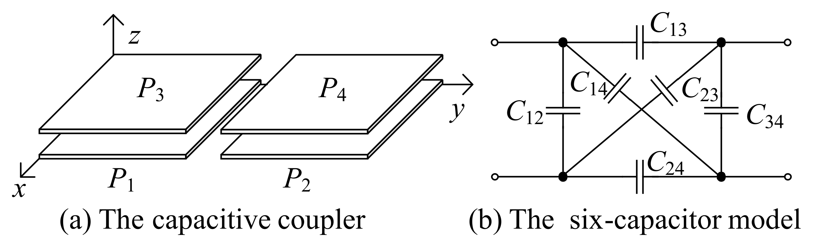
A high operating frequency is needed: Equivalent capacitances of the capacitive coupler are always in pF range in most applications due to the small dielectric constant of air [16,21,22,23]. To eliminate reactive power, the small equivalent capacitances must resonate with a relatively large inductor, which is not expected due to bulky size and corresponding losses, so that CPT converters always work at a high operating frequency.
(2)
The output characteristics of the CPT circuit should be independent of the capacitive coupler parameters: The structure of a capacitive coupler is always constrained by the volume of a CPT system. Thus, the parameters of a capacitive coupler are determined and they cannot be designed to satisfy the charging demands of loads [27].
(3)
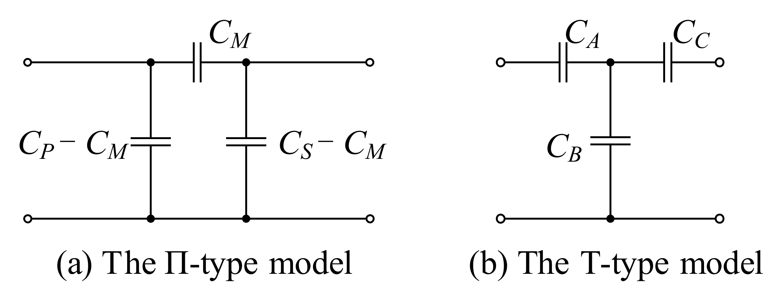
External capacitors are needed to elevate the equivalent capacitances of the capacitive couplers in some situations: With the pF-range equivalent capacitances of the capacitive coupler, it is very difficult to compensate for the reactive power induced by the capacitive coupler. Thus, external capacitors are always added to parallel with the capacitive coupler to elevate the small equivalent capacitances [16,28].
As stated in [22,29], the double-sided LC compensated CPT circuit with four compensation components cannot realize both CC and CV outputs while the input ZPA is guaranteed. As stated in [30], the LCLC-LC compensated CPT circuit with six compensation components has two CC frequencies and one CV frequency to realize input ZPA and load-independent CC and CV outputs. In addition, the CC and CV output gains of the LCLC-LC compensated CPT circuit are adjustable. However, one CC frequency is enough to realize CC output and multiple components in the compensation circuit would increase the system cost and power losses. To satisfy the charging demands of batteries, six constraints should be realized: CC output, CV output, input ZPA at CC mode, input ZPA at CV mode, designable output current, and designable output voltage. In theory, taking CC or CV frequency as a design variable, a CPT circuit with five compensation components may realize desired CC and CV outputs with input ZPA.
In this paper, a CPT circuit with five compensation components is designed to realize both CC and CV outputs. After systematical analyzation, a CC frequency and a CV frequency with input ZPA are derived to realize the predesigned CC and CV outputs. The effect of the change in the length of air gap between the plates on CC/CV condition is studied. To permit the ZVS of MOSFETs in both CC/CV modes, the sensitivities of input impedance and output current or voltage to variations of compensation parameters are analyzed. Finally, a CPT simulation prototype is built to verify the analysis in this paper.

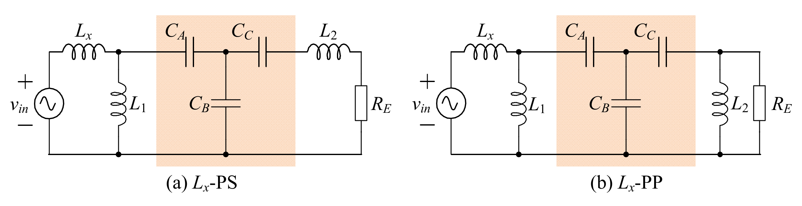
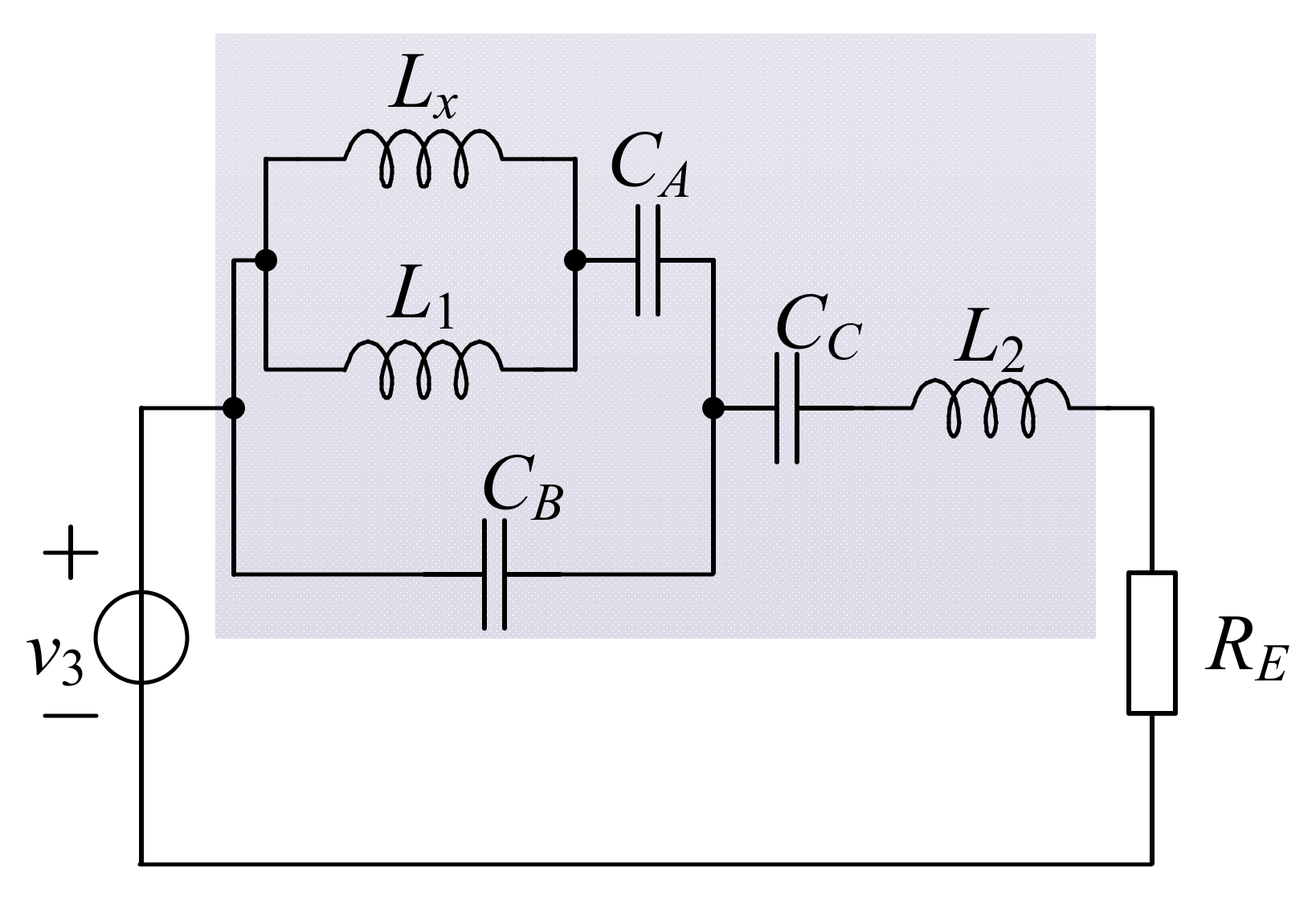
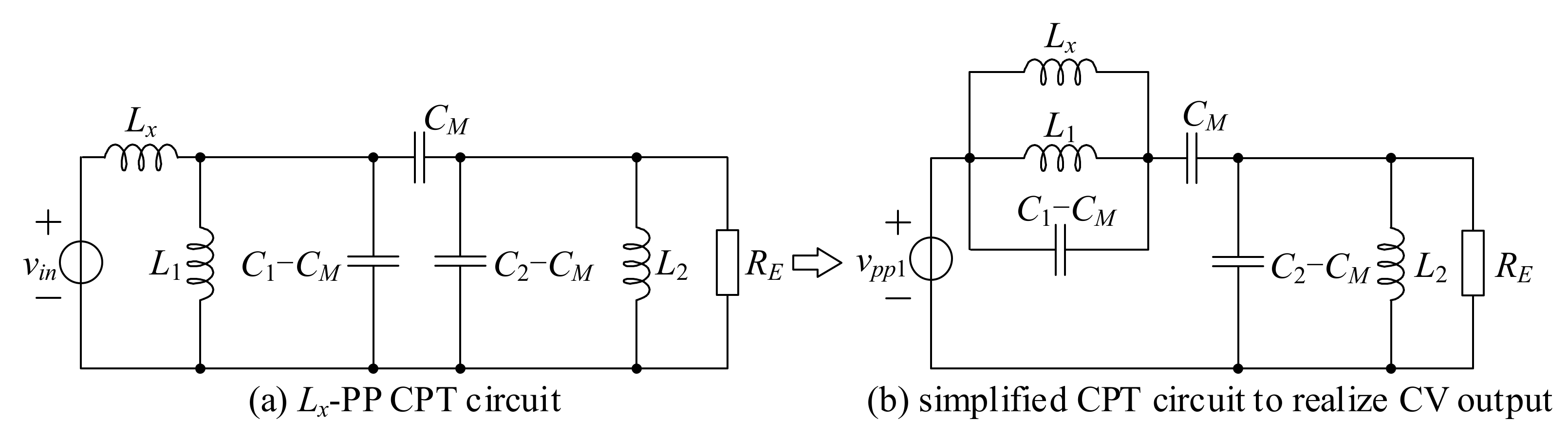
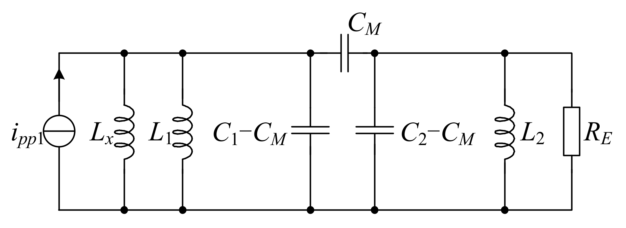
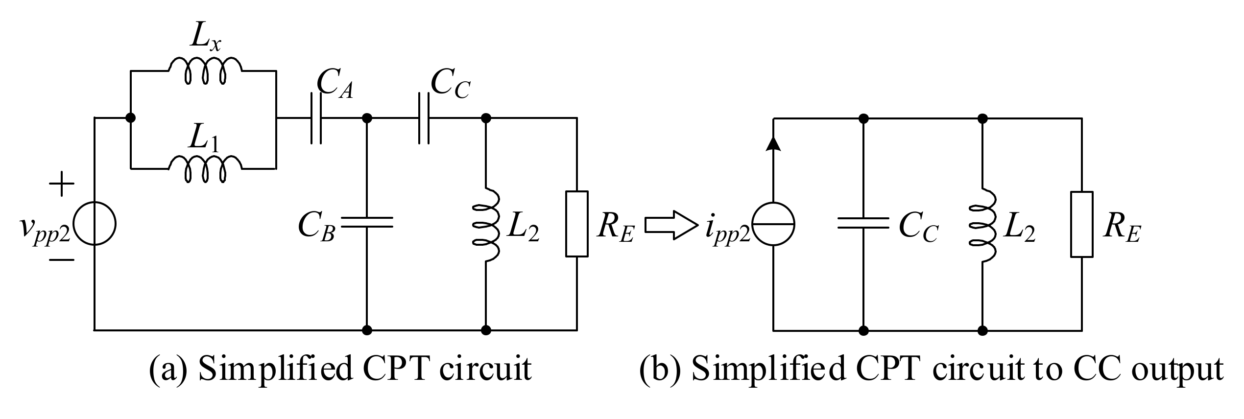
2. Characteristics of the Proposed CPT Circuit

As shown in Figure 1a, the typical capacitive coupler is composed of four metal plates and it can be equivalent to a six-capacitor model where capacitors C12, C13, C14, C23, C24, C34 are formed by plates P1 and P2, P1 and P3, P1 and P4, P2 and P3, P2 and P4, P3 and P4 respectively. Furthermore, the six-capacitor model can be converted to a Π-type model where CP is the primary capacitor, CS is the secondary capacitor, and CM is the mutual capacitor, as shown in Figure 1b.
The relationship between the six-capacitor model and the Π-type model satisfies
C P = C 12 + C 13 + C 14 C 23 + C 24 C 13 + C 14 + C 23 + C 24 C S = C 34 + C 13 + C 23 C 14 + C 24 C 13 + C 14   + C 23 + C 24 C M = C 24 C 13     C 14 C 23 C 13 + C 14 + C 23 + C 24
Since the dielectric constant of air is 8.85 × 10⁻¹² F/m, the capacitors in the six-capacitor model and the Π-type model are always in the pF range. To elevate the equivalent capacitances, external capacitors Cex1 and Cex2 are added to parallel with the capacitive coupler as shown in Figure 2a, defining C1 = CP + Cex1 and C2 = CS + Cex2. To simplify the analysis, the Π-type model together with Cex1 and Cex2 can be further converted to a T-type model as shown in Figure 2b where capacitors CA, CB, and CC satisfy the equation:
C A = C 1 C 2   C M 2 C 1     C M , C B = C 1 C 2   C M 2   C M , C C = C 1 C 2     C M 2 C 2     C M
IPT has four basic compensation circuits, i.e., series-series (SS), series-parallel (SP), parallel-series (PS), and parallel-parallel (PP) as shown in Figure 3, where M is the mutual inductance, LP is the primary self-inductance, LS is the secondary self-inductance, Cpr is the primary compensation capacitor, and Cse is the secondary compensation capacitor. The SS and SP IPT circuits are powered by a high-frequency sinusoidal voltage source and the PS and PP IPT circuits are powered by a high-frequency sinusoidal current source. Taking the capacitive coupler and the external capacitors as a whole, CPT also has four basic compensation circuits as shown in Figure 4 where L1 and L2 are compensation inductors and the capacitive coupler is equivalent to a T-type model.
However, the CPT circuit with four compensation components cannot realize the input ZPA and CC/CV outputs to satisfy the charging demands of batteries. Thus, to prove a CPT circuit with five compensation components can achieve input ZPA and desired output, an additional inductor Lx is added into the PS and PP CPT circuits and these CPT circuits are powered by a high-frequency voltage source, as shown in Figure 5.

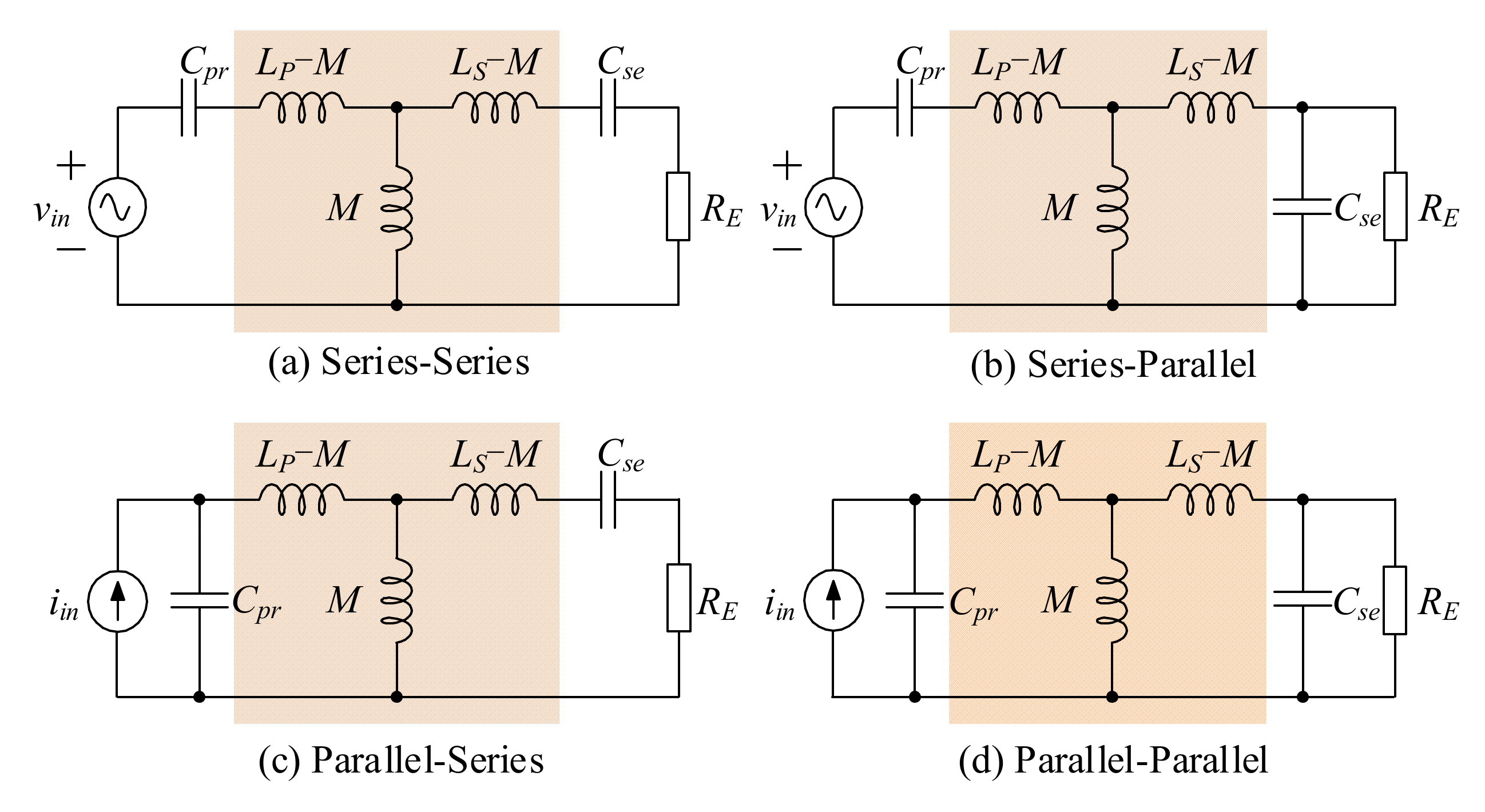
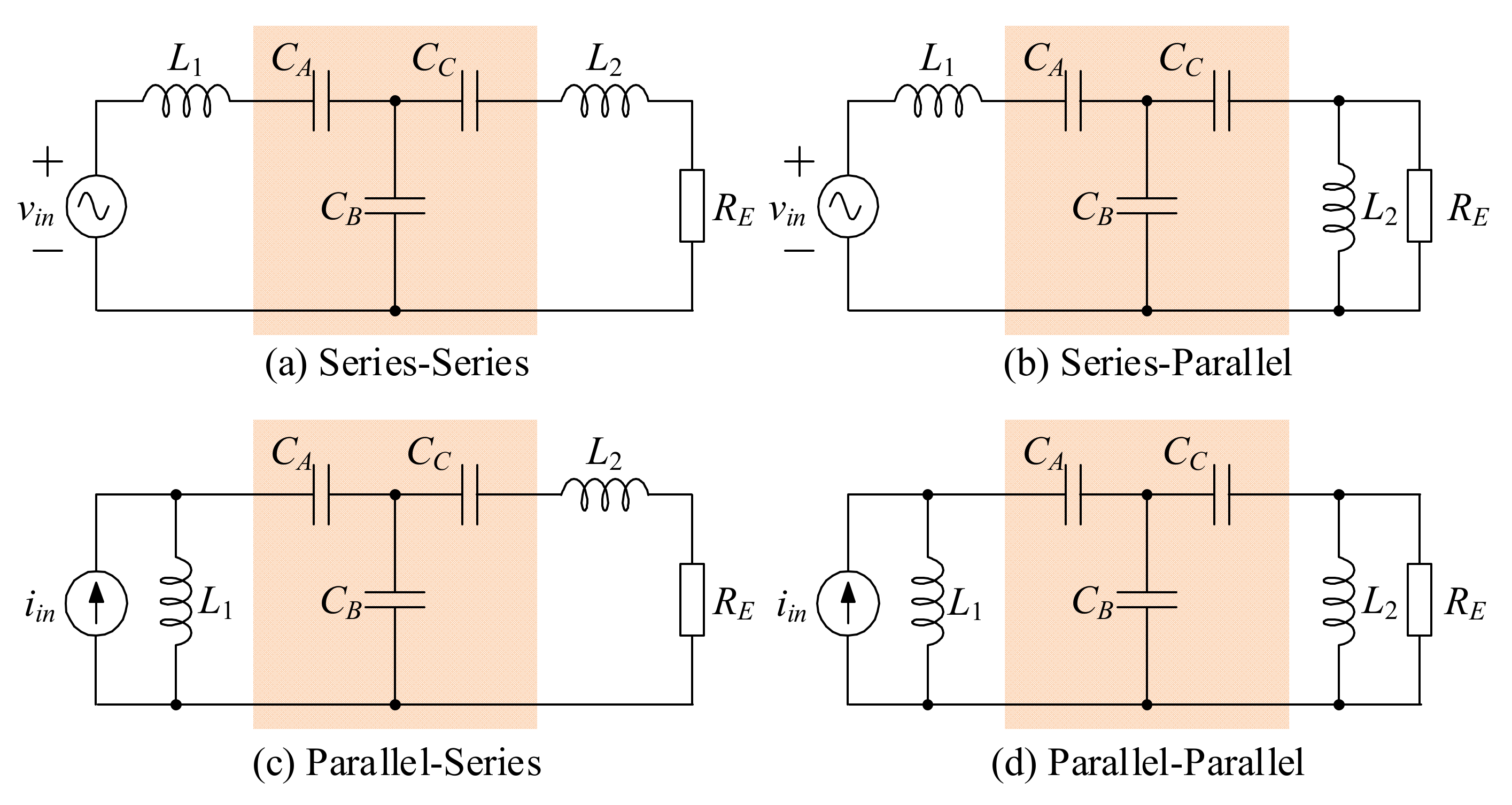
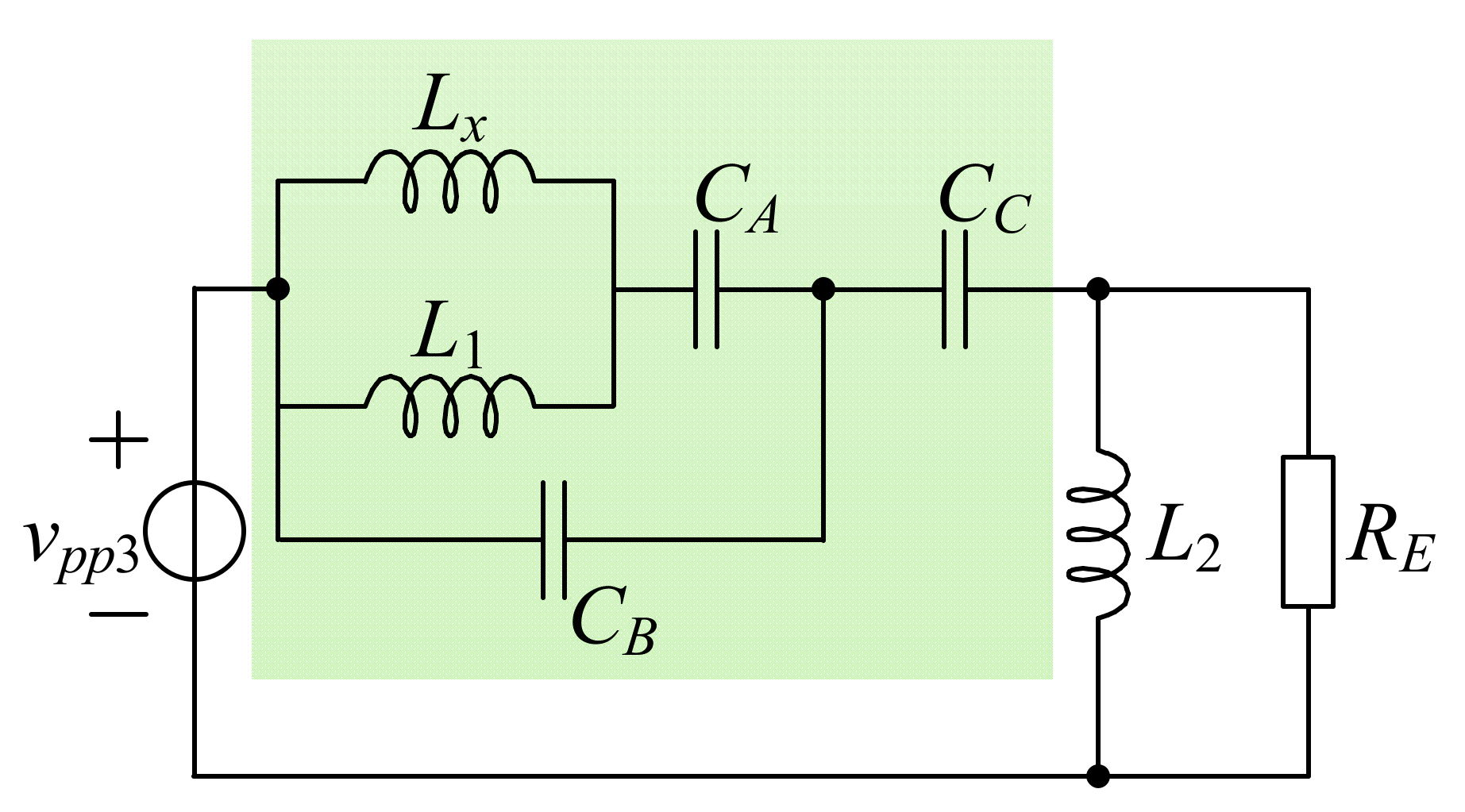
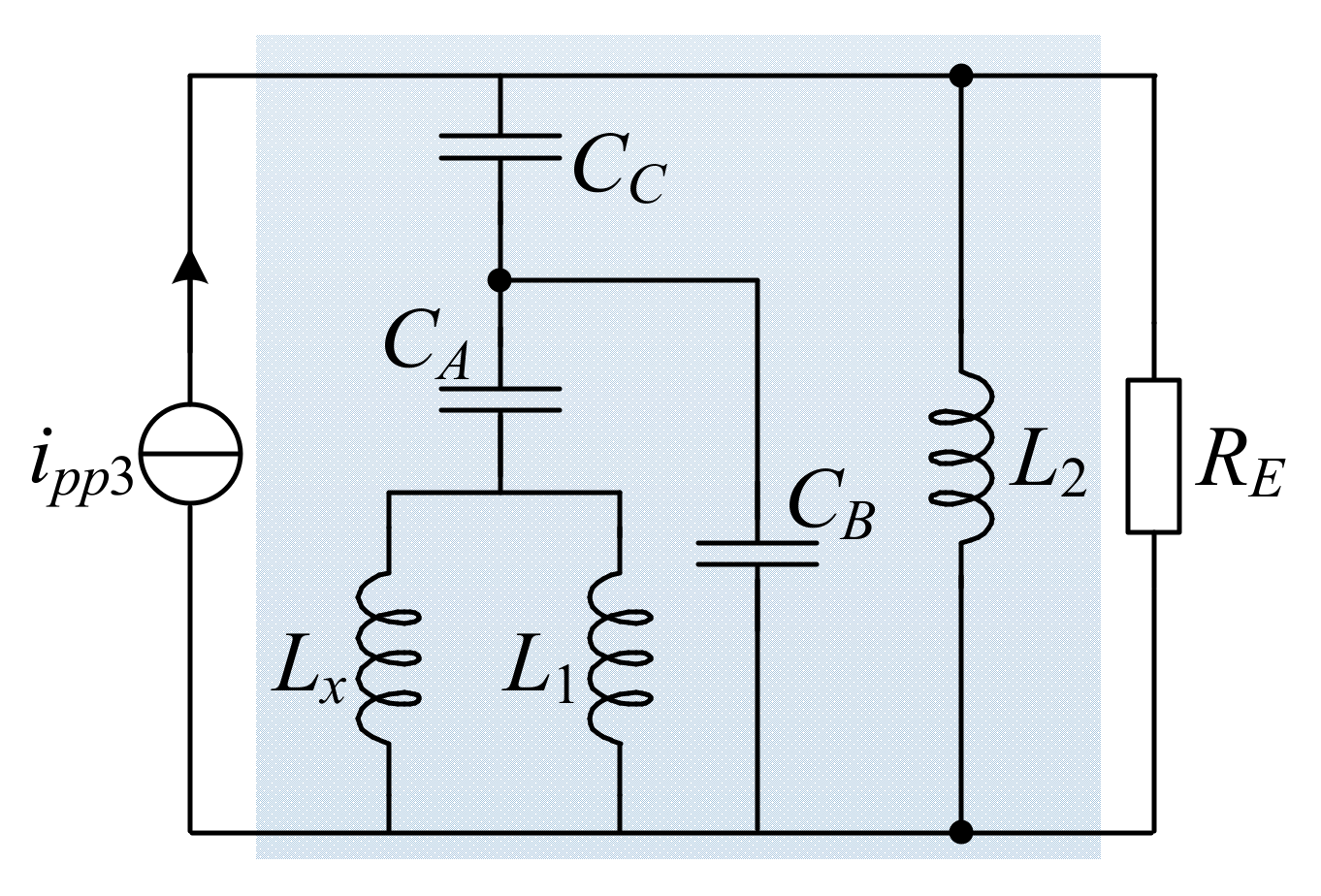
2.1. The Analysis of the Lx-PS CPT Circuit

With the Π-type model of the capacitive coupler, if inductors Lx and L1 resonate with capacitor C1CM, the CPT circuit can be converted to Figure 6b and the power source is equivalent to a current source i1 as shown in Figure 6b. To realize load-independent CV output, inductor L1 should resonate with capacitor C2CM as shown in Figure 6c,d. According to the aforementioned analysis, if the CV angular frequency is defined as ωv, it should satisfy the constraint:
ω v = L 1 + L x L 1 L x ( C 1   C M ) = 1 L 2 ( C 2   C M )
According to Figure 6a, the input impedance Zv at ωv can be simplified as:
Z v = ω v 4 ( C 2   C M ) 2 L x 2 C M R E C M   j ω v ( C 2   C M ) [ C 2   + ω v 2 C M L x ( C 2   C M ) ] R E
To achieve input ZPA, the input impedance Zv should be resistive. Thus, the CV angular frequency ωv should satisfy the constraint:
L x = C 2 ω v 2 C M ( C M     C 2 )
Due to C2 = Cex2 + CP and CP > CM, capacitor CMC2 is smaller than zero. With Lx > 0, the Equation (5) is not valid. Thus, the input ZPA cannot be achieved.
Based on the T-type model of the capacitive coupler and external capacitors, the Lx-PS CPT circuit can be drawn as Figure 7a. If capacitor CA resonates with inductors Lx and L1 and capacitor CC resonates with L2, the CPT circuit in Figure 7b can realize the load-independent CV output. With the aforementioned analysis, if the CV angular frequency is defined as ωv1, it should satisfy the constraint:
ω v 1 = L 1 + L x L 1 L x C A = 1 L 2 C C
According to Figure 7a, the input impedance Zv1 at ωv1 can be simplified as
Z v 1 = ω v 1 4 C A 2 L x 2 R E 1 + j ω v 1 ( C A + C B     ω v 1 2 C A 2 L x ) R E
To obtain a resistive input impedance, the CV angular frequency ωv1 should satisfy:
ω v 1 = C A + C B L x C A 2
Then, Equation (7) is simplified as
Z v 1 = ω v 1 4 C A 2 L x 2 R E
Until now, the input ZPA and CV output of the CPT circuit are all achieved at ωv1. To work at a CC mode, a CC frequency for the Lx-PS CPT circuit with input ZPA and CC output should be derived.
The CPT circuit can be converted to Figure 8. With (CA + LxL1) ‖ CB = ∞, a load-independent CC output is realized. With the aforementioned analysis, if the CC angular frequency is defined as ωc, it should satisfy the constraint:
ω c = 1 C A + 1 C B 1 L 1 + 1 L x
With Figure 8, the input impedance Zc at ωc can be calculated as
Z c = j ω c 3 C M 2 L x 2 C 2 + ω c 2 C M 2 L x     ω c 2 C 2 2 L 2 + j ω c C 2 2 R E
To obtain a resistive input impedance, the CC angular frequency should satisfy:
ω c = C 2 C 2   2 L 2 + C M   2 L x
Then, the input impedance Zc can be simplified as
Z c = ω c 3 C M 2 L x 2 C 2 2 R E
The output current irps can be simplified as
i r p s = j ω c C M 2 C 1 + C 2   2 C M C 2 C 1   C M 1     ω c 2 C 2 L 2 v i n
According to Equations (13) and (14), the input ZPA is realized in the CC mode. With the above analysis, the Lx-PS CPT circuit can realize the input ZPA in both CC and CV modes.
However, according to Equations (6) and (8), there are three constraints for the realization of input ZPA and CV output. As stated in the Introduction, six variables with one frequency and five compensation components are adopted to satisfy six design constraints. Thus, a CV frequency with two constraints to realize the input ZPA at CV mode is needed.
The CPT circuit can be converted to Figure 9. If the impendence of the purple box is zero, the CPT circuit can directly realize load-independent CV output. And the CV angular frequency defining as ωv2 should satisfy
C 1 C 2 C M 2 L 1 L 2 L x ω v 2 4 L 1 L 2 C 2 + L 1 L x C 1 + C 2 L 2 L x ω v 2   2 + L 1   + L x = 0
The input impendence of the Lx-PS CPT circuit at ωv2 is
Z v 2 = ω v 2 4 C M 2 L 1 2 R E ω v 2 4 L 1 L 2 ( C M 2 - C 1 C 2 ) + ω v 2 2 C 1 L 1 + C 2 L 2 - 1 ω v 2 4 L 1 L 2 ( C M 2 - C 1 C 2 ) + ω v 2 2 C 1 L 1 + C 2 L 2 - 1 + j ω R E ( ω v 2 2 C 1 C 2 L 1 - C 2 - ω v 2 2 C M 2 L 1 )
To make Zv2 resistively, ωv2 should satisfy
ω v 2 = C 2 L 1 C 1 C 2 C M 2
Then, Equation (16) is simplified as
Z v 2 = C 2 2 R E C M 2
At ωv2, the load-independent output voltage vr2 is
v r 2 = C M C 2 v i n
According to Equations (15) and (17), the input ZPA is realized in the CV mode. With the above analysis, the Lx-PS CPT circuit can realize the input ZPA in both CC and CV modes with four constraints. According to Equations (14) and (19), the output current at CC mode and the output voltage at CV mode are all adjustable which means the Lx-PS CPT circuit can satisfy the charging demands of different kinds of loads.

2.2. The Analysis of the Lx-PP CPT Circuit

Similar with the Lx-PS CPT circuit, an additional inductor Lx is inserted between the voltage source and the primary side of a PP compensation circuit to form the Lx-PP CPT circuit as shown in Figure 10a. With Figure 10b, if CM resonates with (LxL1C1CM), the input voltage vin can be converted to a load-independent voltage source vpp1. In this way, the CV angular frequency ωcv can be calculated as
ω c v = 1 C 1 1 L 1 + 1 L x
With Figure 10, the input impedance Zcv at ωcv is simplified as
Z c v = j ω c v 5 C M 2 L 2 L x 2 R E j ω c v L 2 + R E 1   ω c v 2 C 2 L 2   + ω c v 2 C M 2 L 2 L x
To eliminate the imaginary part of Zcv, the CV angular frequency ωcv should satisfy
1 + ω c v 4 C M 2 L x ω c v 2 C 2 L 2 = 0
Similarly, with the constrain of Equation (22), the input ZPA at CV mode is achieved. And the simplified input impedance Zcv is simplified as Equation (23).
Z c v = ω c v 4 C M 2 L x 2 R E
Until now, the input ZPA and CV output are realized. According to (24), the output voltage vppr at ωcv is adjustable.
v p p r = v i n ω c v 2 C M L x
If Lx resonates with L1 and C1CM and L2 resonates with C2CM, the Lx-PP CPT circuit is converted to a load-independent current source as shown in Figure 11.
If the CC angular frequency is defined as ωcc, it should satisfy two constraints:
ω c c = 1 C 1 C M 1 L 1 + 1 L x = 1 L 2 C 2 C M
The simplified input impedance Zcc at ωcc is expressed as
Z c c = j ω c c 3 C M L x 2 1 + ω c c 2 C M L x + j ω c c C M R E
The imaginary part of Zcc cannot be eliminated. Thus, the input ZPA cannot be guaranteed.
To derive a CC frequency with a resistive input impedance, the Lx-PS CPT circuit using the T-type model is shown in Figure 5b. As shown in Figure 12a, if CA resonates with Lx paralleling with L1, vin is transformed to a voltage source vpp2. If L2 resonates with CC, the CPT circuit is converted to a load-independent current source as shown in Figure 12b. The CC angular frequency defined as ωcc1 should satisfy
ω c c 1 = 1 C A   1 L 1 + 1 L x = 1 L 2 C C
The input impendence Zcc1 at ωcc1 is simplified as
Z c c 1 = j ω c c 1 3 C A 2 L x 2 j ω c c 1 C C 2 R E   + ω c c 1 2 C A 2 L x   C A     C B   C C
If the CC angular frequency ωcc1 satisfy
ω c c 1 = C 2   C M L x C M C 1 C M  
the input impendence is resistive. Then, Zcc1 is simplified as
Z c c 1 = 1   ω c c 1 2 C M 2 R E  
If the impendence of the green box in Figure 13 is zero, the Lx-PS CPT circuit is converted to a voltage source vpp3. The operating angular frequency ωcv1 is
ω c v 1 = 1 C A + 1 C B + C C 1 L 1 + 1 L x
Since Equation (31) can be simplified as Equation (20), the CV angular frequency ωcv1 is equal to ωcv.
Similar to the angular frequency ωv of the Lx-PS circuit, there are three constraints for the Lx-PP circuit at ωcc1 to realize input ZPA and CC output according to Equations (27) and (29). Thus, a CC frequency with two constraints to realize the input ZPA at CC mode is needed. The CPT circuit can be converted to Figure 14.
If the impendence of the blue box in Figure 14 is infinite, the Lx-PS CPT circuit is converted to a current source ipp3. And the operating angular frequency ωcc2 should satisfy
ω c c 2 4 L 1 L 2 L x C 1 C 2 C M 2 ω c c 2 2 L 1 L 2 C 2 + L 1 C 1 L x + C 2 L 2 L x + L 1 + L x = 0
The simplified impendence of the Lx-PP circuit at ωcc2 is calculated as
Z c c 2 = j ω c c 2 L x + L 1   ω c c 2 2 C 1 L 1 L x 2 L 1   ω c c 2 2 C 1 L 1 2 + L x   2 ω c c 2 2 C 1 L 1 L x + ω c c 2 4 C 1 2 L 1 2 L x + j ω c c 2 3 C M 2 L 1 2 R E
To realize input ZPA, the Lx-PP circuit at ωcc2 should satisfy
ω c c 2 = 1 C 1 L 1
Then Equation (33) can be calculated as
Z c c 2 = 1 ω c c 2 2 C M 2 R E
And the expression of output current icc2 is
i c c 2 = j ω c c 2 C M v i n
As mentioned above, the mutual capacitance CM of a regular capacitive coupler is always in pF-range. Thus, according to (36), even if the CV frequency is MHz-level, the output current icc2 is relatively small, which cannot satisfy the charging demands of most loads. With the aforementioned analysis, the Lx-PP CPT circuit cannot realize desired outputs at both CC and CV modes.

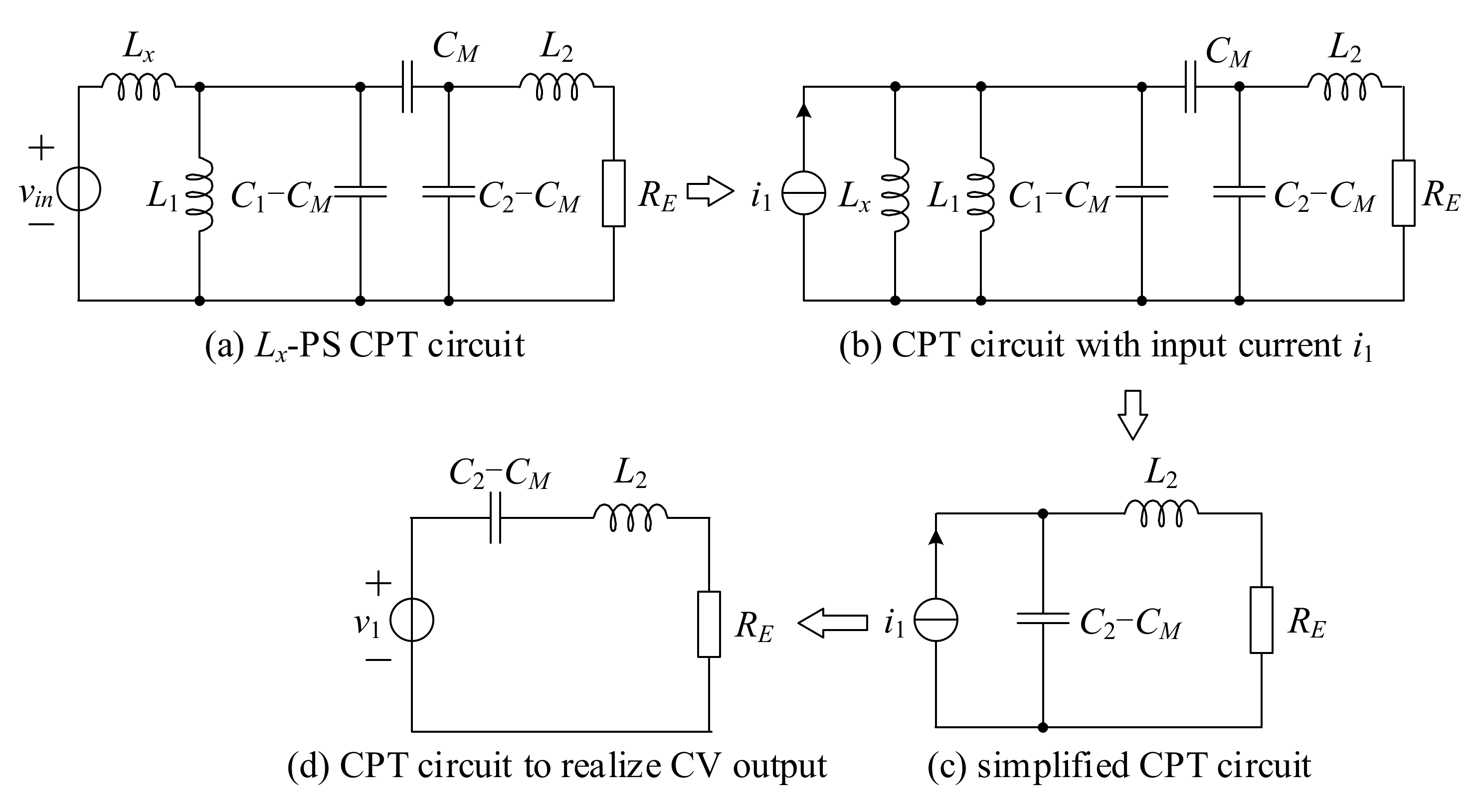
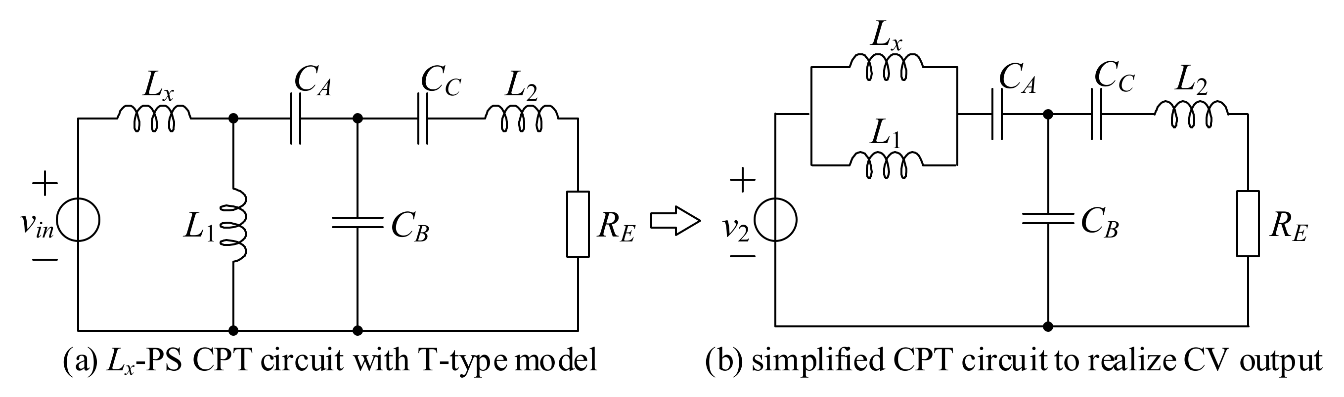
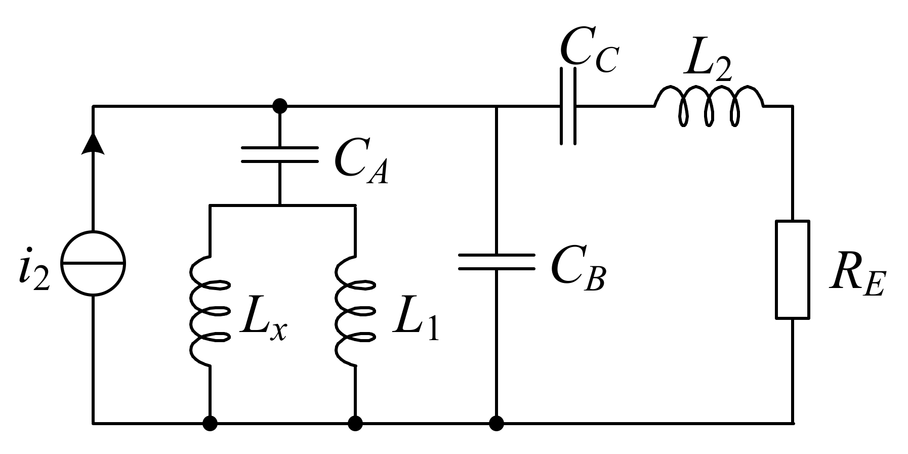
3. Parameter Design Procedure of the Lx-PS CPT Circuit

As analyzed in Section 2, the Lx-PS CPT circuit can satisfy the charging demands of batteries. The schematic of a Lx-PS CPT circuit is shown as Figure 15. The whole circuit is powered by a direct voltage VDC. The inverter uses a full-bridge inverter. The rectification uses a full-bridge rectifier and a filter capacitor. The voltage VDC is converted to a high-frequency square-wave voltage vAB by the inverter. The fundamental component of vAB is vin which is calculated as
v i n ( t ) = 4 V D C π s i n π D 2 s i n ω t
And D is the duty cycle of vAB. The load of the whole circuit is RL. The relationship between RL and RE is
R L = π 2 8 R E
Since the maximum value of ir is Ir, the relationship between IO and Ir is
I O = 2 π I r
Since the maximum value of vr is Vr, the relationship between VO and Vr is
V O = π 4 V r
As analyzed in Section 2, the CC angular frequency ωc and the CV angular frequency ωv2 are chosen as the operating frequencies of the Lx-PS CPT circuit. Given the load-required output current IO and output voltage VO, the compensation parameters Lx, L1, L2, C1, and C2 of the Lx-PS compensation circuit can be calculated as Equations (41)–(45) by the constraints of Equations (10)–(19).
L x = C 2 ω c 2   ω v 2 2 2 C M 2 ω c 2 ω v 2 2
L 1 = C 2 ω c 2   ω v 2 2 2 2 C M 2 ω c 2 ω v 2 4
L 2 = ω c 2 + ω v 2 2 2 C 2 ω c 2 ω v 2 2
C 1 = 4 ω c 4 + ω v 2 4 C M V O π ω c 2   ω v 2 2 2 V D C
C 2 = π C M V D C 4 V O
The relationship between ωc and ωv2 can be simplified as
ω v 2 = π ω c I O π 2 I O + 16 ω c C M V D C
Until now, with predesigned CC angular frequency ωc, output current IO, and the output voltage VO, the CV angular frequency ωv2 and compensation parameters Lx, L1, L2, C1, and C2 are all determined. The output current iO and the output voltage vO can be simplified as
i O = 16 π 2 ω c ω v 2 2 C M V D C j ω c 2   ω v 2 2
v O = 8 π 2 C 2 2 R L C M 2
With predesigned CC angular frequency ωc and the expression of Equation (47), the output current iO at CC mode is adjustable by changing the CV angular frequency ωv2. Similarly, the output voltage vO at CV mode is also adjustable by changing the compensation parameter C2. The output current iO at CC mode is in direct proportion to ωv2 and the output voltage vO at CV mode is in direct proportion to C2. Thus, the maximum power of the Lx-PS CPT circuit is limited by the insulating properties of the whole system and the actual output power is determined by the charging demands of loads.
Thus, the Lx-PS CPT circuit can be designed to charge lithium batteries.

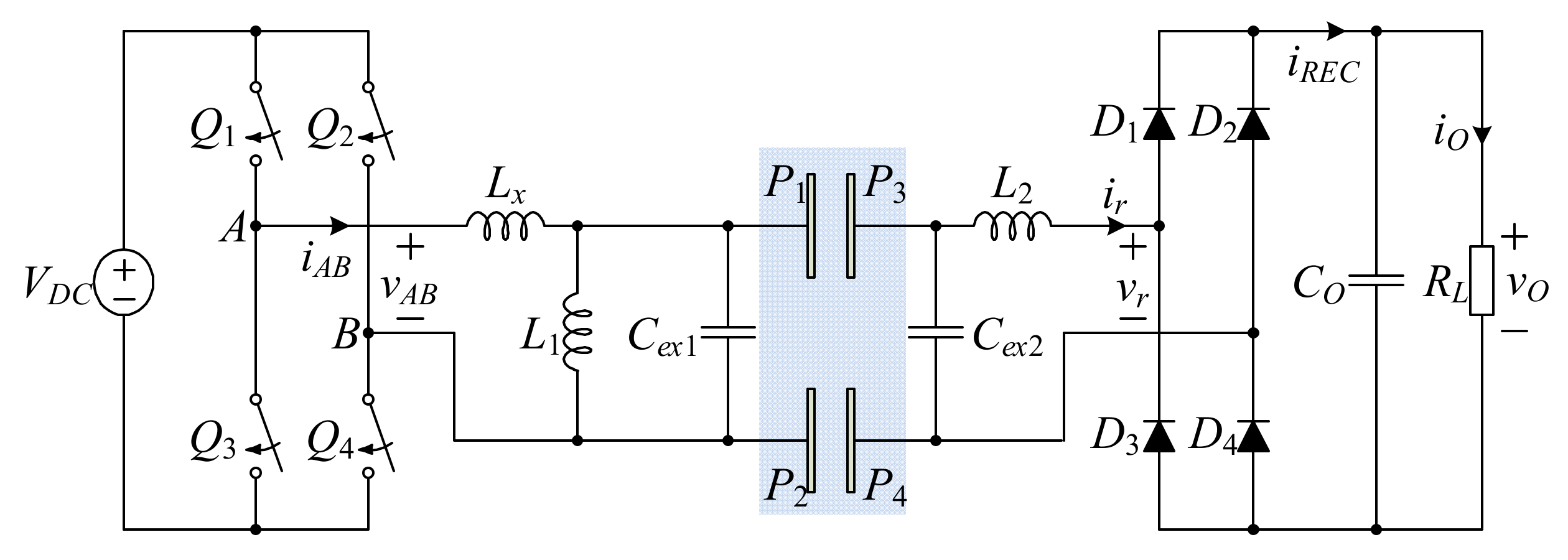
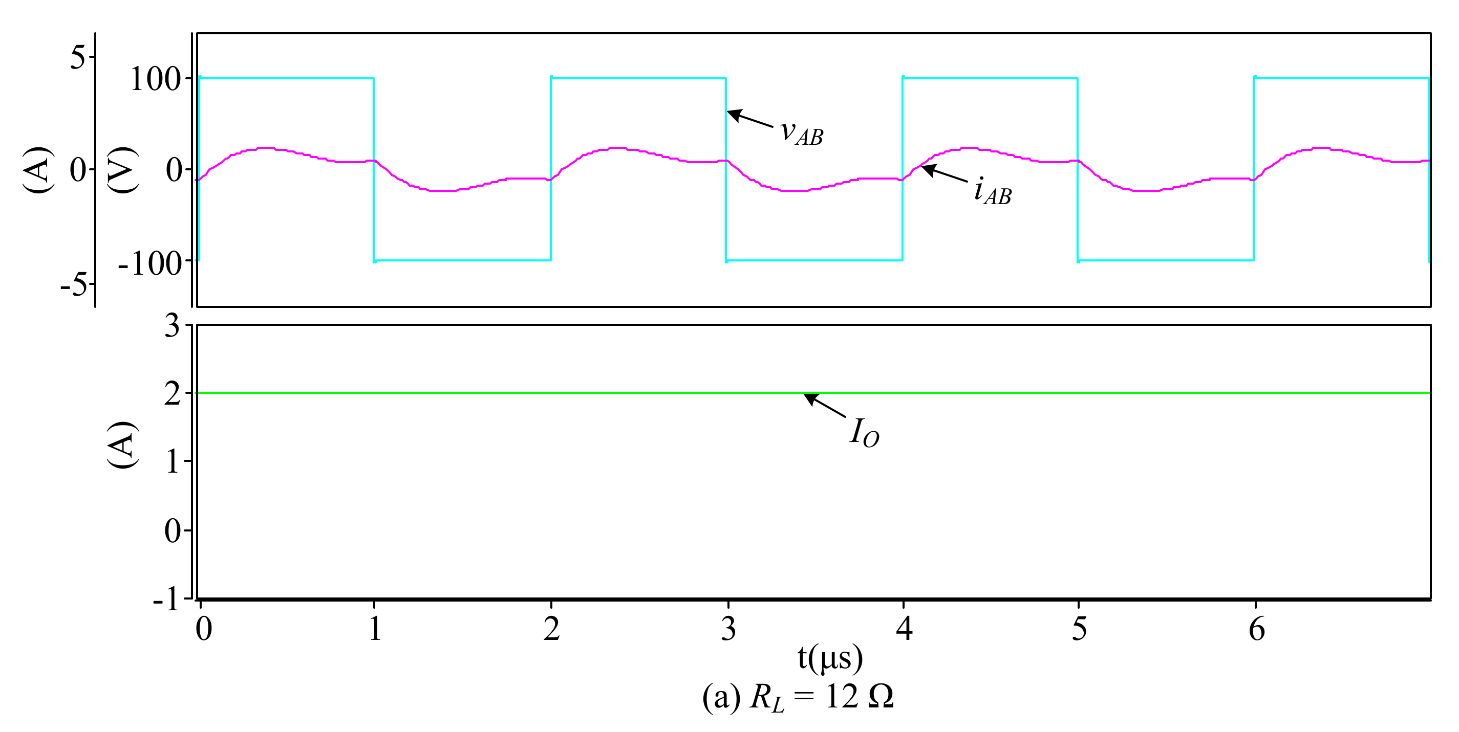
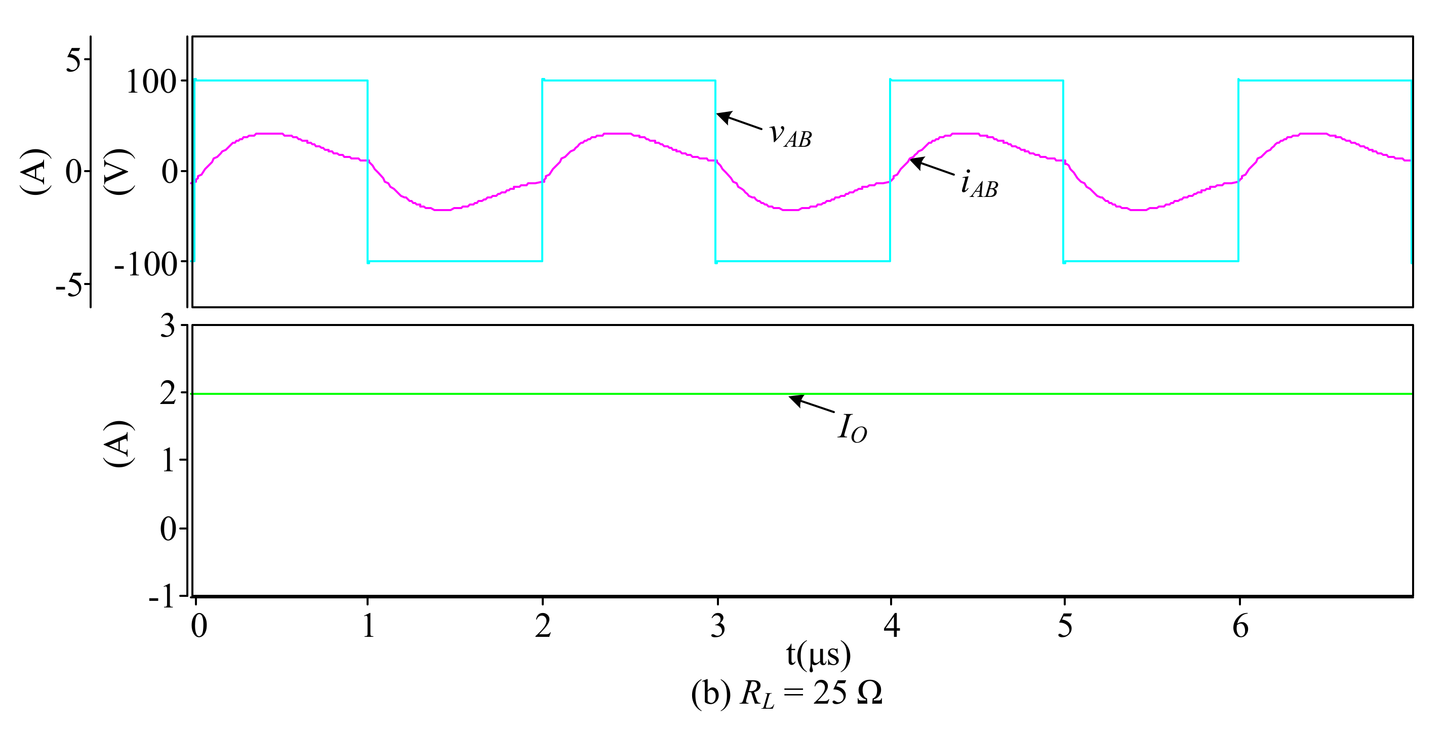
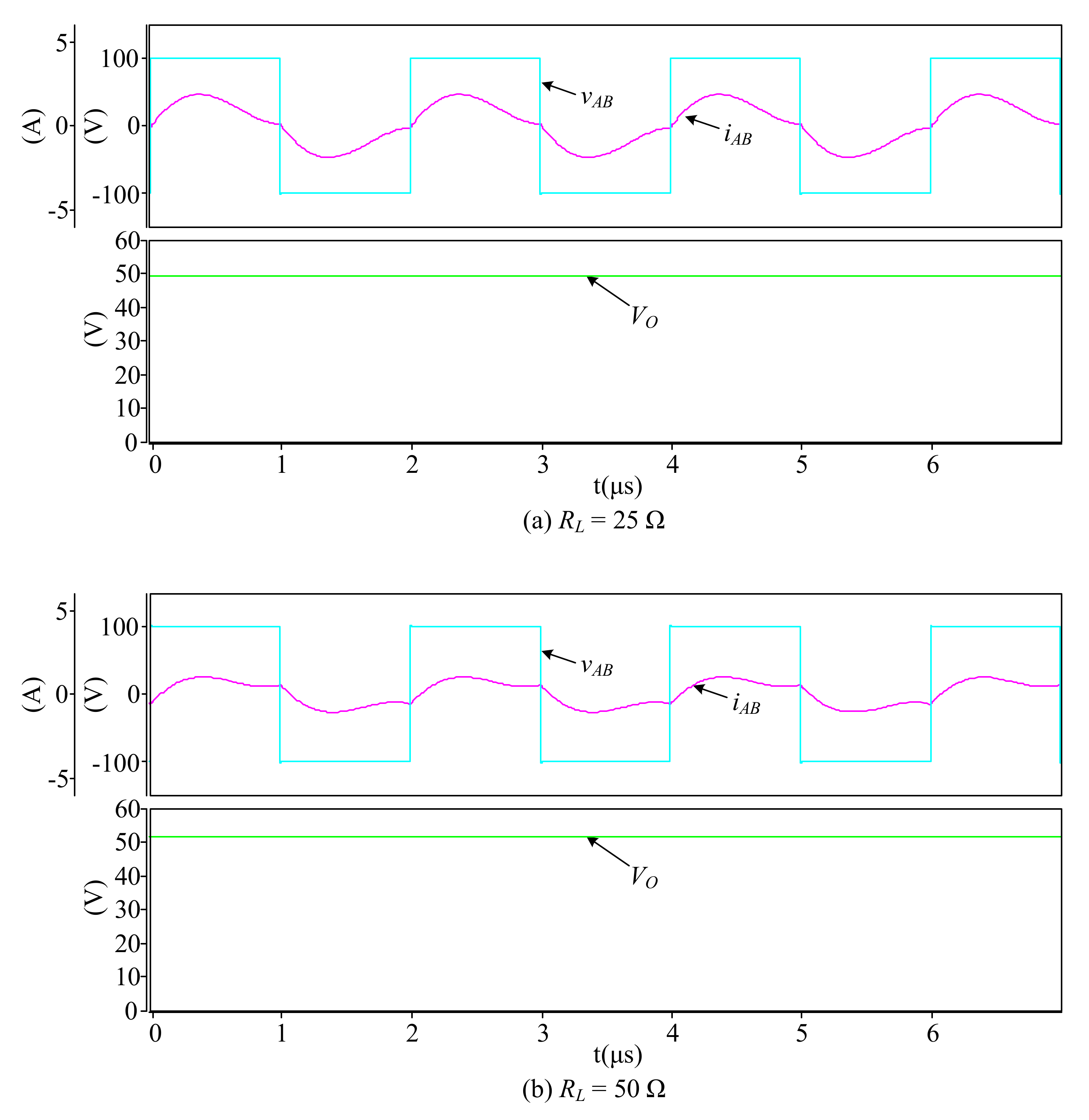
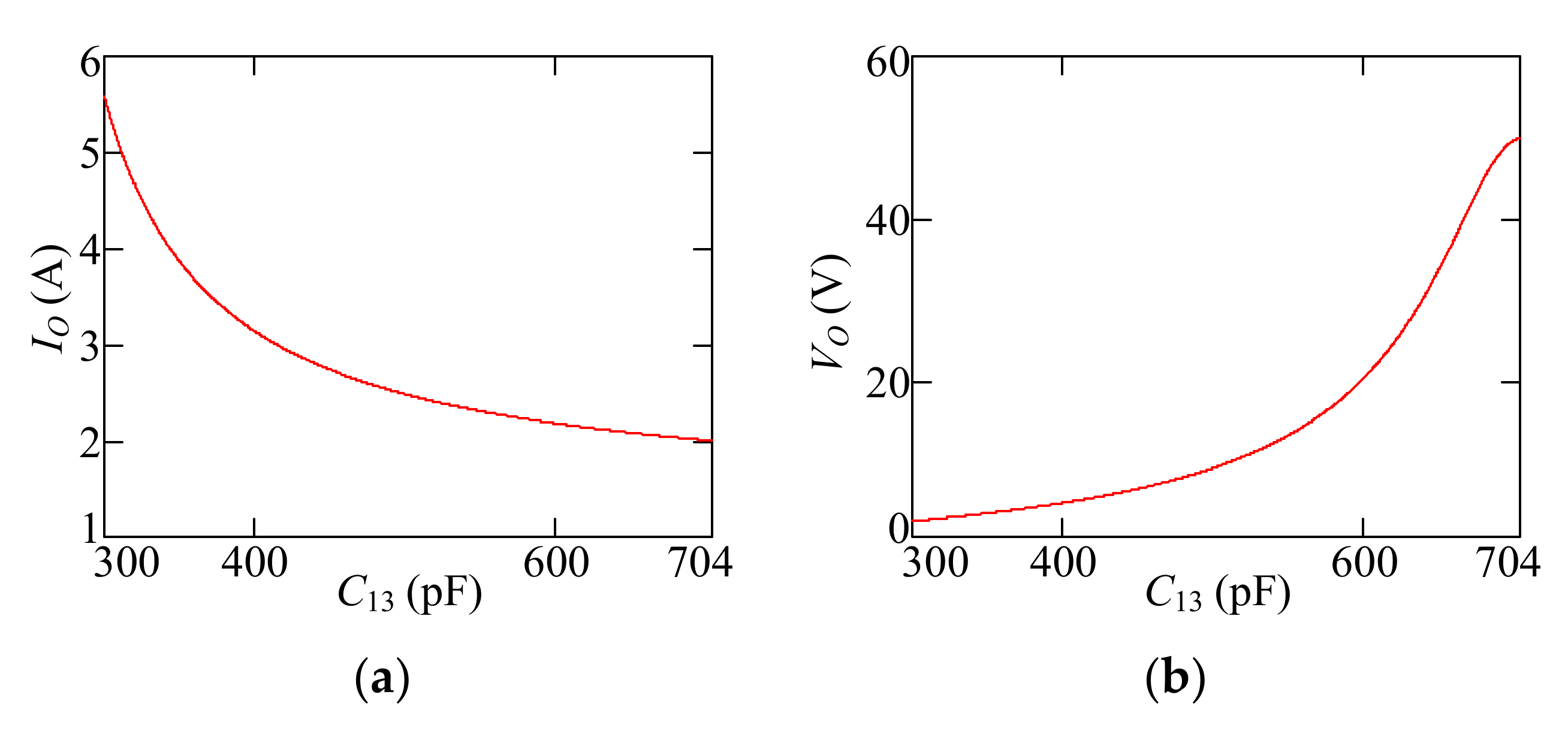
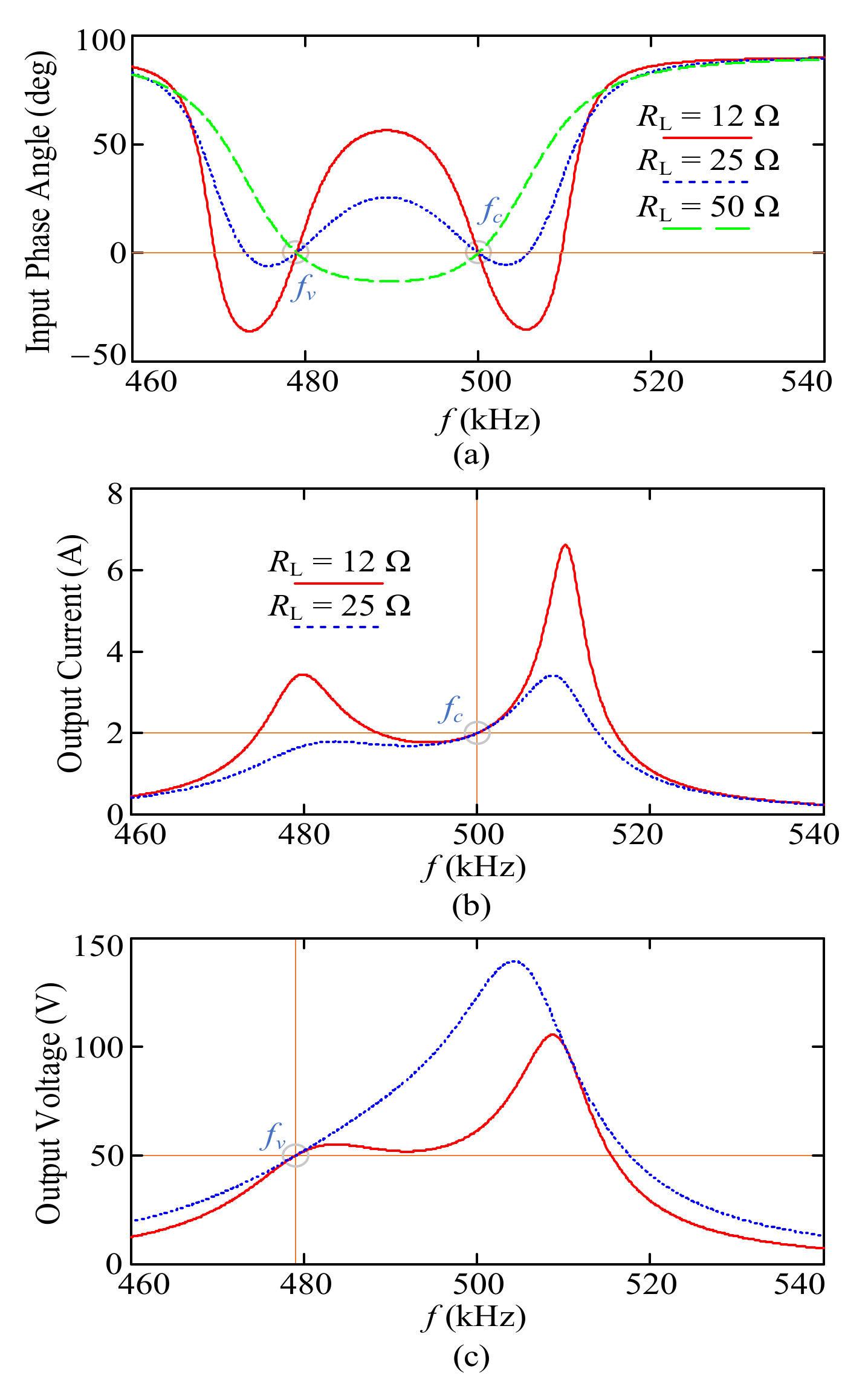
4. Certification of the Proposed Lx-PS CPT Circuit
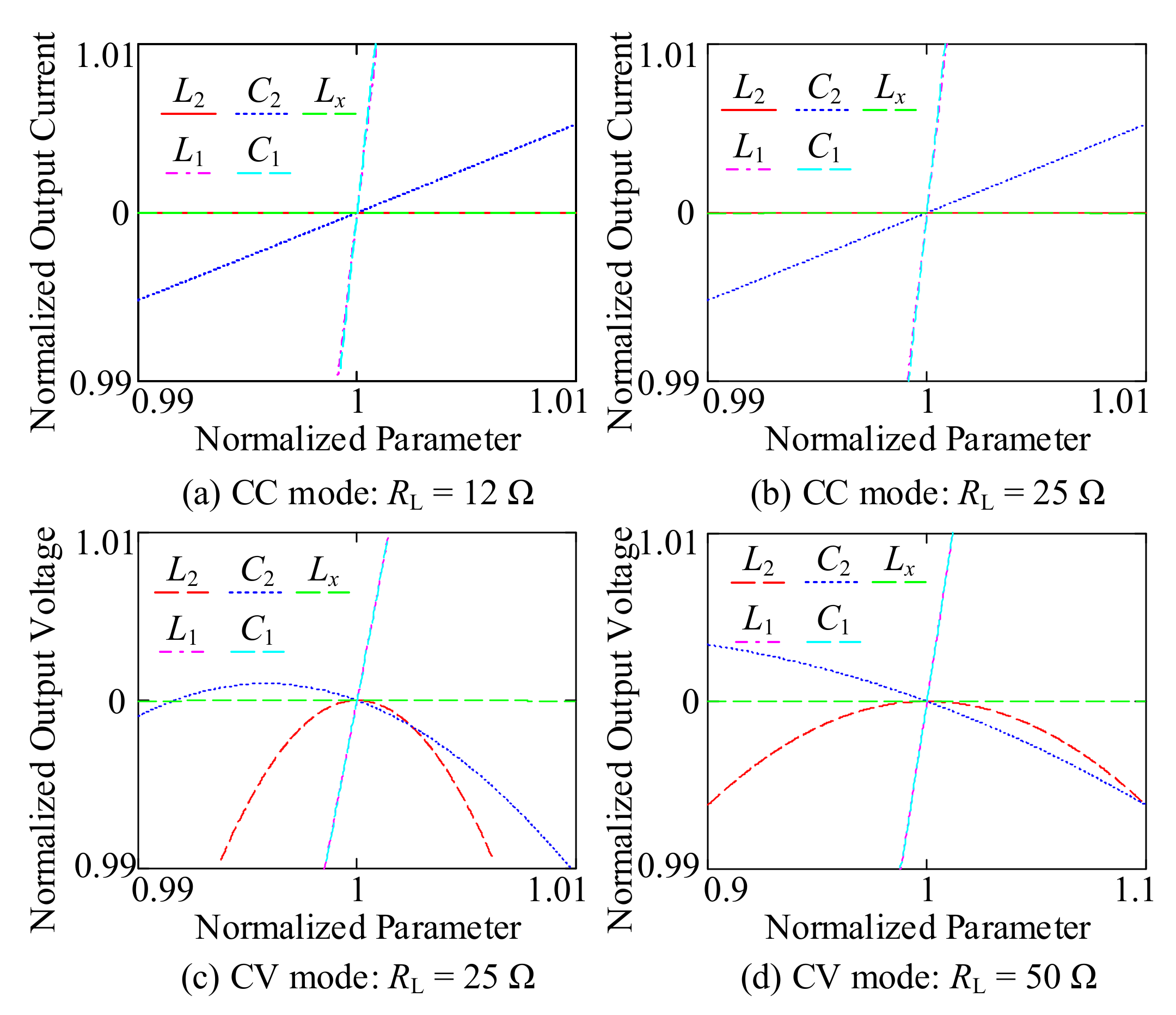
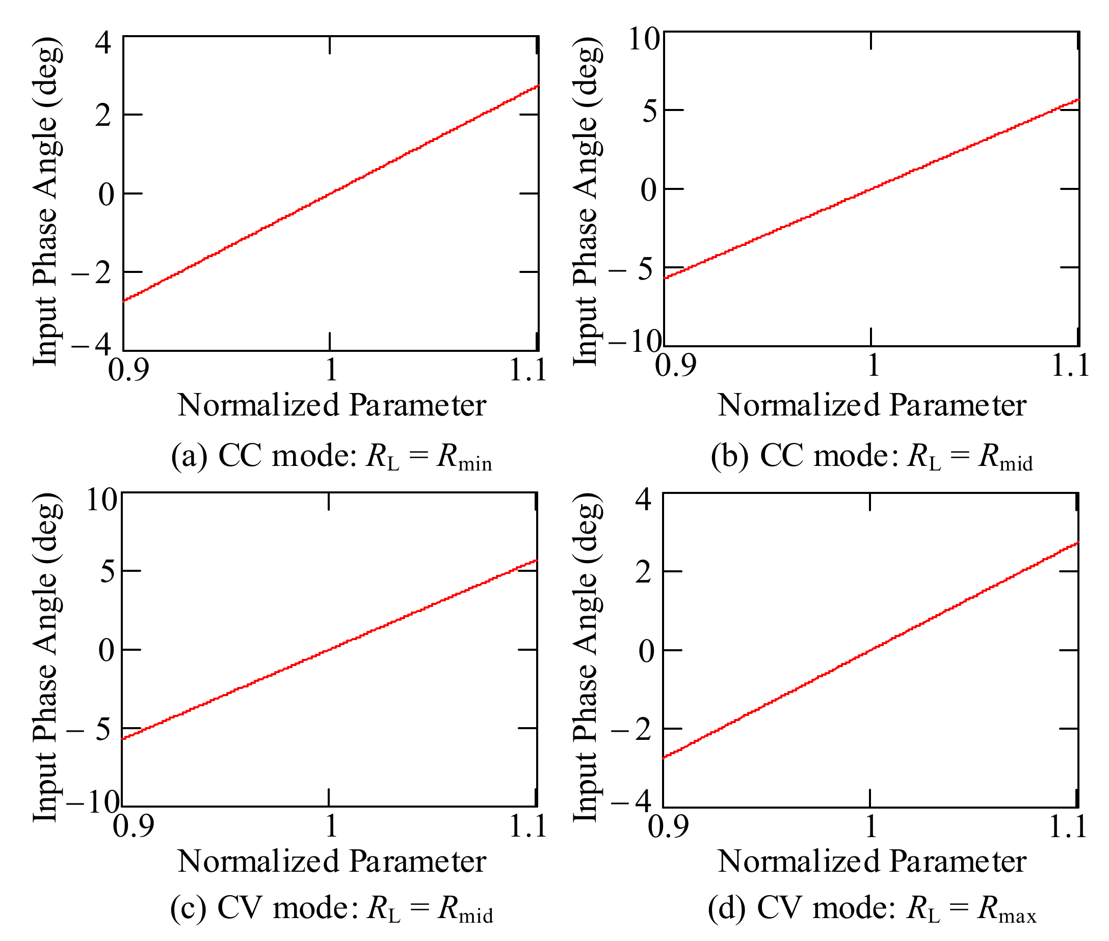
To verify the above analysis, a Lx-PS CPT circuit is designed. The constant output current is 2 A and the constant output voltage is 50 V. The CC operating frequency fc is designed as 500 kHz and the input voltage VDC is chosen as 100 V. The structure of the capacitive coupler is shown as Figure 1a. The power transfer distance is designed as 1 mm. The plates of the capacitive coupler are aluminum and the length of a plate is 380 mm. The distance between plate P1 and plate P2 or plate P3 and plate P4 is 10 mm. The power transfer distance is 18 mm. The mutual capacitance CM is 352.2 pF, the primary and secondary capacitances CP and CS are 352.6 pF and 352.7 pF. With the predesigned output current, output voltage, the CC operating frequency, and the capacitive coupler, the CV operating frequency and compensation parameters can be calculated by Equations (37)–(48), which have been summarized in Table 1.
According to Figure 16, the output current keeps at 2 A when RL is equal to 12 Ω or 25 Ω, which means the CC output is successfully achieved. The input voltage vAB is in phase with the input current iAB, which means the input ZPA is achieved and most reactive power is eliminated.
According to Figure 17, when the operating mode of the Lx-PS CPT circuit is transferred to CV mode, the output voltages at 25 Ω and 50 Ω are all 50 V. Similarly, the load-independent CV output is achieved and the input ZPA is guaranteed.
However, the power transfer distance may change during the power transmission process. Since the metal plates P1, P2, P3, and P4 are the same size, capacitors C13 = C24, C12 = C34, and C14 = C23. Compared to C13 and C24, C14 and C24 are negligible. Then, Equation (1) can be approximately simplified as
C P = C 12 + C 13 2 C S = C 12 + C 13 2 C M = C 13 2
Based on the CV operating frequency and compensation parameters shown in Table 1, the effect of the change in the length of air gap between the plates on CC/CV conditions is shown in Figure 18.
With the increasing of the air gap, the capacitance C13 would decrease. As shown in Figure 18, the output current increases at CC mode and the output voltage decreases at CV mode.
Figure 19 gives the curves of input phase angle, output current and voltage varying with the operating frequency, which can also verify the theoretical design.
If the plate misalignment happens, the secondary plates of P3 and P4 may move in X-axis or Y-axis direction as shown in Figure 1a. Thus, capacitances C13, C24, C14, and C23 would change. Taking P3 and P4 moving in X-axis as an example, the cross-coupling capacitors C14 and C23 are still negligible. Similar with the aforementioned analysis, C13 and C24 decrease when the plate misalignment happens. Based on the CV operating frequency and compensation parameters shown in Table 1, the output current at CC mode would increase and the output voltage at CV mode would decrease.
To permit ZVS of MOSFETs Q1,2,3,4, the input impedance should be slightly inductive in both CC and CV modes. Figure 20 shows the output current or voltage versus the different normalized parameters and load conditions for the two modes of operation. From Figure 20a,b in CC mode, the output current is not sensitive to the variation of L2 and Lx. From Figure 20c,d in CV mode, the output voltage is not sensitive to the variation of Lx. Thus, Lx is chosen to realize the ZVS of MOSFETs in the two modes of operation. Figure 21 shows the input phase angle versus normalized parameters at two charging modes and two loading conditions. A slight variation of Lx can permit a slight inductive phase angle for ZVS operation.

5. Discussion

A high-performance CPT circuit should be designed to realize input ZPA and load-independent outputs. Since lithium-ion batteries have been universally used, many CPT circuits have been proposed in different research to fulfill the charging demands of batteries.
The proposed Lx-PS CPT circuit can realize input ZPA and CC/CV outputs. Moreover, the output current and output voltage of the proposed circuit are all adjustable, which means the Lx-PS CPT circuit can satisfy the charging demands of different loads. Above all, to reduce the redundancy of the CPT system, the Lx-PS CPT circuit only has five compensation components. Compared to previous research, the number of compensation components is minimum and the whole CPT charger is designed considering all constraints of CPT technology.

6. Conclusions

An Lx-PS CPT circuit with only five compensation components is proposed in this paper to fulfill the charging profile of lithium-ion batteries. A CC frequency and a CV frequency with input ZPA and desired output gain are all derived. An Lx-PS CPT circuit with output current of 2 A and output voltage of 50 V was built and simulation was done to prove the analysis in this paper. According to simulation waveforms, CC output and CV output were all achieved. The input ZPA was realized in both CC and CV modes, which means the input reactive power was zero. Finally, the charging demands of batteries were fulfilled and the redundancy of the CPT circuit was successfully reduced.

Author Contributions

Methodology, B.D.; validation, Y.C.; writing-original draft, J.L.; supervision, X.Q. All authors have read and agreed to the published version of the manuscript.

Funding

This research received no external funding.

Institutional Review Board Statement

Not applicable.

Informed Consent Statement

Not applicable.

Data Availability Statement

Not applicable.

Conflicts of Interest

The authors declare no conflict of interest.

References

  1. Hou, J.; Chen, Q.; Zhang, Z.; Wong, S.C.; Tse, C.K. Analysis of output current characteristics for higher order primary compensation in inductive power transfer systems. IEEE Trans. Power Electron. 2018, 33, 6807–6821. [Google Scholar] [CrossRef]
  2. Chen, C.; Kou, Z.; Zhang, Y.; He, Z.; Mai, R.; Cao, G. Hybrid topology with configurable charge current and charge voltage output-based WPT charger for massive electric bicycles. IEEE J. Emer. Sel. Topics Power Electron. 2018, 6, 1581–1594. [Google Scholar] [CrossRef]
  3. Samanta, S.; Rathore, A.K. A new inductive power transfer topology using direct AC–AC converter with active source current wave shaping. IEEE Trans. Power Electron. 2018, 33, 5565–5577. [Google Scholar] [CrossRef]
  4. Lu, M.; Ngo, K.D.T. Systematic design of coil in series-series inductive power transfer for power transferability and efficiency. IEEE Trans. Power Electron. 2018, 33, 3333–3345. [Google Scholar] [CrossRef]
  5. Yao, Y.; Gao, S.; Wang, Y.; Liu, X.; Zhang, X.; Xu, D. Design and optimization of an electric vehicle wireless charging system using interleaved boost converter and flat solenoid coupler. IEEE Trans. Power Electron. 2021, 36, 3894–3908. [Google Scholar] [CrossRef]
  6. Ahmad, S.; Hattori, R.; Muharam, A. Generalized circuit model of shielded capacitive power transfer. Energies 2021, 14, 2826. [Google Scholar] [CrossRef]
  7. Minnaert, B.; Mastri, F.; Stevens, N.; Costanzo, A.; Mongiardo, M. Coupling-independent capacitive power transfer using frequency bifurcation. Energies 2018, 11, 1912. [Google Scholar] [CrossRef] [Green Version]
  8. Minnaert, B.; Costanzo, A.; Monti, G.; Mongiardo, M. Capacitive wireless power transfer with multiple transmitters: Efficiency optimization. Energies 2020, 13, 3482. [Google Scholar] [CrossRef]
  9. Zhang, Z.; Pang, H.; Georgiadis, A.; CeCati, C. Wireless power transfer-an overview. IEEE Trans. Ind. Electron. 2019, 66, 1044–1058. [Google Scholar] [CrossRef]
  10. Qu, X.; Han, H.; Wong, S.C.; Tse, C.K.; Chen, W. Hybrid IPT topologies with constant current or constant voltage output for battery charging applications. IEEE Trans. Power Electron. 2015, 30, 6329–6337. [Google Scholar] [CrossRef]
  11. Tran, D.H.; Vu, V.B.; Choi, W. Design of a high-efficiency wireless power transfer system with intermediate coils for the on-board chargers of electric vehicles. IEEE Trans. Power Electron. 2018, 33, 175–187. [Google Scholar] [CrossRef]
  12. Kim, M.; Joo, D.M.; Lee, B.K. Design and control of inductive power transfer system for electric vehicles considering wide variation of output voltage and coupling coefficient. IEEE Trans. Power Electron. 2019, 34, 1197–1208. [Google Scholar] [CrossRef]
  13. Qu, X.; Chu, H.; Wong, S.C.; Tse, C.K. An IPT battery charger with near unity power factor and load-independent constant output combating design constraints of input voltage and transformer parameters. IEEE Trans. Power Electron. 2019, 34, 7719–7727. [Google Scholar] [CrossRef]
  14. Lecluyse, C.; Minnaert, B.; Kleemann, M. A review of the current state of technology of capacitive power transfer. Energies 2021, 14, 5862. [Google Scholar] [CrossRef]
  15. Luo, B.; Long, T.; Guo, L.; Dai, R.; Mai, R.; He, Z. Analysis and design of inductive and capacitive hybrid wireless power transfer system for railway application. IEEE Trans. Ind. Appl. 2020, 56, 3034–3042. [Google Scholar] [CrossRef]
  16. Lu, F.; Zhang, H.; Mi, C.C. A review on the recent development of capacitive wireless power transfer technology. Energies 2017, 10, 1752. [Google Scholar] [CrossRef] [Green Version]
  17. Lin, C.-H.; Amir, M.; Tariq, M.; Shahvez, M.; Alamri, B.; Alahmadi, A.; Siddiqui, M.; Beig, A.R. Comprehensive analysis of IPT v/s CPT for Wireless EV Charging and Effect of Capacitor Plate Shape and Foreign Particle on CPT. Processes 2021, 9, 1619. [Google Scholar] [CrossRef]
  18. Luo, B.; Hu, A.P.; Munir, H.; Zhu, Q.; Mai, R.; He, Z. Compensation network design of CPT systems for achieving maximum power transfer under coupling voltage constraints. IEEE J. Emer. Sel. Topics Power Electron. 2022, 10, 138–148. [Google Scholar] [CrossRef]
  19. Zhang, H.; Lu, F. An improved design methodology of the double-sided LC-compensated CPT system considering the inductance detuning. IEEE Trans. Power Electron. 2019, 34, 11396–11406. [Google Scholar] [CrossRef]
  20. Wang, Y.; Zhang, H.; Lu, F. Review, analysis, and design of four basic CPT topologies and the application of high-order compensation networks. IEEE Trans. Power Electron. 2022, 37, 6181–6193. [Google Scholar] [CrossRef]
  21. Li, S.; Liu, Z.; Zhao, H.; Zhu, L.; Shuai, C.; Chen, Z. Wireless power transfer by electric field resonance and its application in dynamic charging. IEEE Trans. Ind. Electron. 2016, 63, 6602–6612. [Google Scholar] [CrossRef]
  22. Lu, F.; Zhang, H.; Hofmann, H.; Mi, C.C. A double-sided LC compensation circuit for loosely-coupled capacitive power transfer. IEEE Trans. Power Electron. 2018, 33, 1633–1643. [Google Scholar] [CrossRef]
  23. Mai, R.; Luo, B.; Chen, Y.; He, Z. Double-sided CL compensation topology based component voltage stress optimisation method for capacitive power transfer charging system. IET Power Electron. 2018, 11, 1153–1160. [Google Scholar] [CrossRef]
  24. Qing, X.; Wang, Z.; Su, Y.; Zhao, Y.; Wu, X. Parameter design method with constant output voltage characteristic for bilateral LC-compensated CPT system. IEEE J. Emer. Sel. Topics Power Electron. 2020, 8, 2707–2715. [Google Scholar] [CrossRef]
  25. Lu, J.; Zhu, G.; Lin, D.; Zhang, Y.; Jiang, J.; Mi, C.C. Unified load-independent ZPA analysis and design in CC and CV modes of higher order resonant circuits for WPT systems. IEEE Trans. Transport. Electrific. 2019, 5, 977–987. [Google Scholar] [CrossRef]
  26. Lu, J.; Zhu, G.; Lin, D.; Zhang, Y.; Wang, H.; Mi, C.C. Realizing constant current and constant voltage outputs and input zero phase angle of wireless power transfer systems with minimum component counts. IEEE Trans. Intell. Transp. Syst. 2021, 22, 600–610. [Google Scholar] [CrossRef]
  27. Zhang, H.; Lu, F.; Hofmann, H.; Liu, W.; Mi, C.C. Six-plate capacitive coupler to reduce electric field emission in large air-gap capacitive power transfer. IEEE Trans. Power Electron. 2018, 33, 665–675. [Google Scholar] [CrossRef]
  28. Corti, F.; Reatti, A.; Wu, Y.; Czarkowski, D.; Musumeci, S. Zero voltage switching condition in class-E inverter for capacitive power transfer applications. Energies 2021, 14, 911. [Google Scholar] [CrossRef]
  29. Lian, J.; Qu, X. Design of a double-sided LC compensated capacitive power transfer system with capacitor voltage stress optimization. IEEE Trans. Circuits Syst. II Exp. Briefs. 2020, 67, 715–719. [Google Scholar] [CrossRef]
  30. Lian, J.; Qu, X. An LCLC-LC compensated capacitive power transferred battery charger with near unity power factor and configurable charging profile. IEEE Trans. Ind. Appl. 2022, 58, 1053–1060. [Google Scholar] [CrossRef]
Figure 1. A typical structure of the capacitive coupler and its six-capacitor model.
Energies 15 01523 g001
Figure 2. The equivalent model of the capacitive coupler.
Energies 15 01523 g002
Figure 3. Four basic inductive power transfer (IPT) circuits.
Energies 15 01523 g003
Figure 4. Four basic capacitive power transfer (CPT) circuits.
Energies 15 01523 g004
Figure 5. Lx-PS and Lx-PP CPT circuits.
Energies 15 01523 g005
Figure 6. The Lx-PS CPT circuit using the Π-type model to realize constant voltage (CV) output.
Energies 15 01523 g006
Figure 7. The Lx-PS CPT circuit using the T-type model to realize CV output.
Energies 15 01523 g007
Figure 8. The simplified Lx-PS CPT circuit using the T-type model to realize constant current (CC output).
Energies 15 01523 g008
Figure 9. The simplified Lx-PS CPT circuit using the T-type model to realize CV output.
Energies 15 01523 g009
Figure 10. The Lx-PP CPT circuit and its equivalent circuit.
Energies 15 01523 g010
Figure 11. The simplified Lx-PP CPT circuit using Π-type model to realize CC output.
Energies 15 01523 g011
Figure 12. The simplified Lx-PP CPT circuit using the T-type model to realize CC output.
Energies 15 01523 g012
Figure 13. The simplified Lx-PP CPT circuit using the T-type model to realize CV output.
Energies 15 01523 g013
Figure 14. The simplified Lx-PP CPT circuit using T-type model to realize CC output.
Energies 15 01523 g014
Figure 15. The Lx-PS CPT circuit.
Energies 15 01523 g015
Figure 16. The waveforms of the Lx−PS CPT circuit at CC mode.
Energies 15 01523 g016aEnergies 15 01523 g016b
Figure 17. The waveforms of the Lx−PS CPT circuit at CV mode.
Energies 15 01523 g017
Figure 18. The effect of the change in the length of air gap between the plates on CC/CV conditions. (a) the output current at CC mode (b) the output voltage at CV mode.
Energies 15 01523 g018
Figure 19. Curves of (a) input phase angle, (b) output constant current, (c) output constant voltage versus the operating frequencies at CC/CV modes.
Energies 15 01523 g019
Figure 20. Output current or voltage versus normalized parameters at two charging modes and two loading conditions.
Energies 15 01523 g020
Figure 21. Input phase angle versus normalized parameters at two charging modes and two loading conditions.
Energies 15 01523 g021
Table 1. The CV operating frequency and compensation parameters.
ParameterCV FrequencyLxL1L2C1C2
Value479 kHz25.8 μH2.31 μH150.5 μH47.9 nF704 pF
Publisher’s Note: MDPI stays neutral with regard to jurisdictional claims in published maps and institutional affiliations.

