
Effect of Device Scaling on Electron Mobility in Nanoscale GaN HEMTs with Polarization Charge Modulation

1
Institute of Novel Semiconductors, Shandong University, Jinan 250100, China
2
Department of Electrical and Computer Engineering, University of Delaware, Newark, DE 19716, USA
*
Authors to whom correspondence should be addressed.
Nanomaterials 2022, 12(10), 1718; https://0-doi-org.brum.beds.ac.uk/10.3390/nano12101718
Submission received: 9 April 2022
/
Revised: 11 May 2022
/
Accepted: 12 May 2022
/
Published: 18 May 2022
(This article belongs to the Special Issue Electronic Nanodevices)
Abstract
:We have experimentally investigated the impact of vertical and lateral scaling on low-field electron mobility (µ) in InAlN/GaN high-electron-mobility transistors (HEMTs). It is found that µ reduces as InAlN barrier (TB) and gate length (LG) scale down but increases with the scaled source–drain distance (LSD). Polarization Coulomb Field (PCF) scattering is believed to account for the scaling-dependent electron mobility characteristic. The polarization charge distribution is modulated with the vertical and lateral scaling, resulting in the changes in µ limited by PCF scattering. The mobility characteristic shows that PCF scattering should be considered when devices scale down, which is significant for the device design and performance improvement for RF applications.
1. Introduction
Due to the high breakdown voltage, high two-dimensional electron gas densities, and high electron saturation velocity, gallium nitride (GaN) high-electron-mobility transistors (HEMTs) have been ideal for high-frequency and high-power applications, such as radar communications, electronic countermeasures, 5G applications, small base stations, new communication microsatellites, power transmission and automotive electronics [1,2,3,4,5]. Yan Tang et al. fabricated the AlN/GaN/AlGaN double heterojunction HEMTs with fully passivation and n+-GaN ohmic contact regrowth technology, demonstrating a record high current/power gain cutoff frequency fT/fmax of 454/444 GHz on a 20 nm-gate-length HEMT with gate–source and gate–drain spacings of 50 nm [6]. Jeong-Gil Kim et al. reported an AlGaN/GaN HEMT structure on the high-quality undoped thick AlN buffer layer with a high breakdown voltage of 2154 V and a very high figure of merit (FOM) of ~1.8 GV2·Ω−1·cm−2 [7]. Xiaoyu Xia et al. reported a new type of AlGaN/GaN HEMTs with a microfield plate (FP) with a breakdown voltage increase from 870 V to 1278 V by adjusting the distribution of the potential and channel electric field [8]. Maddaka Reddeppa et al. demonstrated high photoresponse and the electrical transport properties of a pristine GaN nanorod-based Schottky diode with an optimized Schottky barrier height [9]. Kedhareswara Sairam Pasupuleti et al. developed the integration of conductive polypyrrole (Ppy) and GaN nanorods for high-performance self-powered UV-A photodetectors, exhibiting superior photoresponse properties such as detectivity, responsivity, external quantum efficiency, good stability and reproducibility [10].
To further improve device performance, device scaling in GaN HEMTs is necessary [6,11,12]. The effects of scaling on short-channel effects (SECs), leakage current, electron velocity, frequency characteristics have been studied [13,14,15,16,17,18], providing insightful guidance for device design and performance improvement. However, few studies about the impact of scaling on electron mobility have been reported. In general, low-field mobility should not change when devices scale down. However, due to the spontaneous and piezoelectric polarization in GaN HEMTs, there are polarization charges in the barrier layer [19,20], which is different from conventional transistors (Si, GaAs, et al.). The change in the polarization charge distribution is related to the device dimension and can result in scattering on the channel electrons [21,22], which leads to a possible change in mobility with device scaling. In this article, to demonstrate this influence, the InAlN/GaN HEMTs with various barrier thicknesses, source–drain distances, and gate lengths are fabricated and the effect of scaling on electron mobility is studied.
2. Experiment
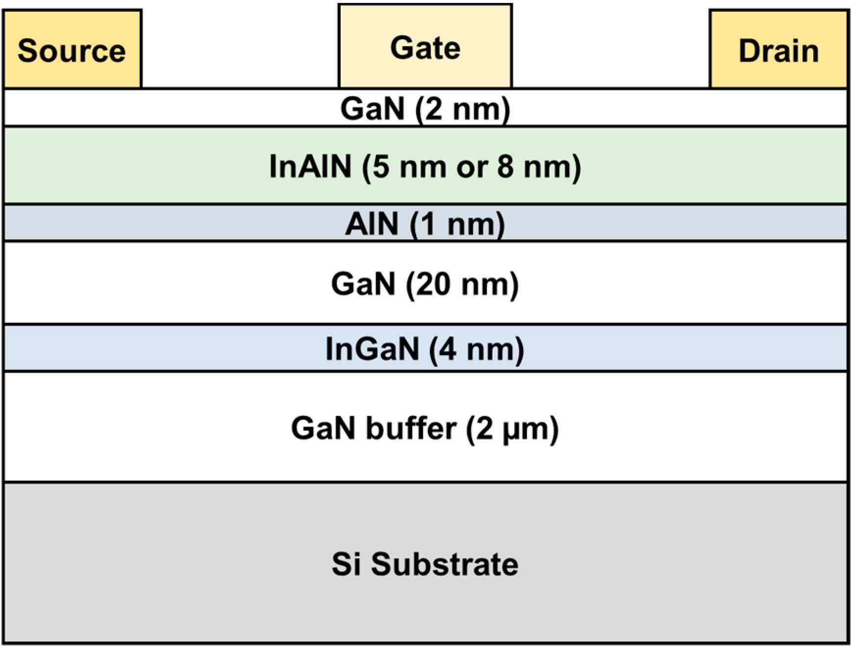
The lattice-matched In0.17Al0.83N/GaN HEMT structure is grown by metal–organic chemical vapor deposition on a Si substrate, as shown in Figure 1, consisting of a 2 nm GaN cap, an InAlN barrier, a 1 nm AlN interlayer, a 15 nm GaN channel layer, a 4 nm In0.12Ga0.88N back-barrier and a 2 μm undoped GaN buffer. Here, two different InAlN layers with the thicknesses of 8 nm and 5 nm are grown. The device process started with mesa isolation with Cl2-based inductively coupled plasma (ICP) etching. Then, Ohmic contact was formed with Ti/Al/Ni/Au metal deposition and annealed at 850 °C for 40 s. Ni/Au gate Schottky contact was deposited in the center of the source–drain region to complete the process. For the large devices, the gate length (LG), gate–source distance (LGS), and gate–drain distance (LGD) of the devices are all 2 µm. For the RF devices, two types of devices are fabricated. For type I, LG of the devices is fixed at 50 nm and LSD is 2, 1, and 0.6 µm, respectively. For type II, LSD of the devices is fixed at 1 µm and LG is 50, 100, and 150 nm, respectively. Here, the gate of all the devices is located between the source and drain regions, and the gate width is 2 × 20 µm. The current–voltage (I–V) and capacitance–voltage (C–V) measurements were carried out by using an Agilent B1500A semiconductor parameter analyzer (Agilent Technologies, Santa Clara, CA, USA).
3. Results and Discussion
Figure 2a,b show the measured capacitances (C) of the InAlN/GaN circle diodes with both InAlN barrier thicknesses (TB). Here, six devices are measured and a good consistency is presented. An improved C and a subthreshold voltage (VT) shift are observed due to the reduced InAlN barrier thickness (C = ε/TB, ε is the dielectric constant of InAlN barrier). Through integrating C-V curves, electron density (n2D) is extracted as shown in Figure 2c,d. It shows that the InAlN/GaN heterostructure with 8 nm InAlN barrier presents higher electron density. Figure 3 shows the simulated band structure and 2DEG electron density as a function of the distance from the material surface of the InAlN/GaN heterostructure, which is calculated by self-consistently solving Schrodinger’s and Poisson’s equations [23,24]. Compared with the 5 nm InAlN barrier, the InAlN/GaN heterostructure with an 8 nm InAlN barrier also shows a higher electron density peak. In GaN HEMTs, the surface states are identified as the source of channel electrons. Due to the spontaneous polarization filed, the increase in InAlN barrier thickness can increase the energy of the surface states, resulting in higher electron density [25,26].
Figure 4 shows the output characteristics of the InAlN/GaN HEMTs with different InAlN thickness. The LG, LGS, and LGD of the devices are all 2 µm. To extract low-field mobility, the drain current (ID) at VDS = 0.1 V in the output characteristics are used. At VGS = 0 V, the total source–drain resistance (RSD) can be written as
where RC is the ohmic contact resistance, q is the electron charge, and µ0 and n2D0 are the electron mobility and electron density under the gate region with VGS = 0 V. Here, only µ0 and RC are unknown. Electron mobility in GaN HEMTs is limited by polar optical phonon (µPOP), polarization Coulomb field (µPCF), acoustic phonon (µAP), interface roughness (µIFR), and dislocation (µDIS) scatterings [22,27,28]. PCF scattering is related to the nonuniformity of polarization charge distribution [21,22]. At VGS = 0 V, the polarization charge distribution is uniform, and the PCF can be neglected. Based on the two-dimensional (2D) scattering theory and the obtained n2D0 [27], µ0 can be calculated with 1/µ0 = 1/µPOP + 1/µAP + 1/µIFR + 1/µDIS, and then RC can be determined with (1). Based on the obtained n2D0 and µ0, the electron mobility µ under the gate region under different VGS can be extracted from
Figure 5 depicts the extracted µ versus VGS for both samples. At VGS = 0 V, µ of the devices with 8 nm InAlN and 5 nm InAlN is 1221 and 1651 cm2/V∙s, respectively. The improved electron mobility with a thinner barrier is also confirmed with the Hall measurement (1242 cm2/V∙s for 8 nm InAlN and 1663 cm2/V∙s for 5 nm InAlN) and the electron mobility of Fat-FETs (with LG of 96 µm and LSD of 100 µm, 1101 cm2/V∙s for 8 nm InAlN and 1670 cm2/V∙s for 5 nm InAlN) [29].
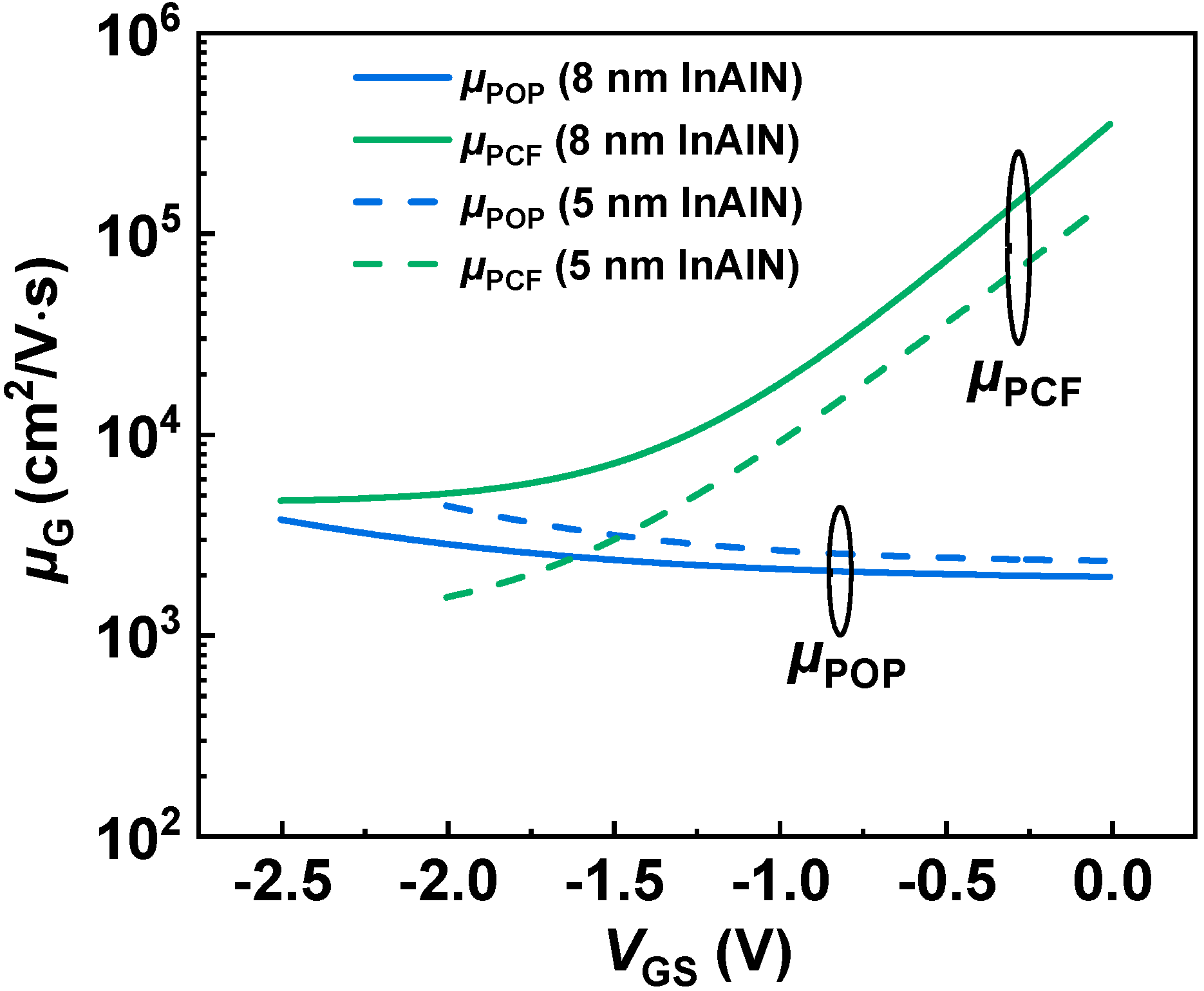
As shown in Figure 5, µ presents a different trend versus VGS for the devices with different InAlN thickness. As VGS increases, µ of the device with 8 nm InAlN deceases, but that of the device with 5 nm InAlN increases. Figure 6a,b show the calculated µ limited by different scatterings for both devices [21,30,31]. The calculated µ (µCAL, lines in the figures) by using 2D scattering theory shows good agreement with the extracted µ (scatters in the figures), which proves the accuracy of the calculation. As VGS increases, µPOP and µIFR decrease, µDIS and µPCF increase, and µAP presents a slight change. µPOP and µPCF play more significant roles among all the scatterings. Figure 7 compares µPOP and µPCF for both devices. When the InAlN barrier decreases from 8 nm to 5 nm, µPOP increases while µPCF decreases. The reduced n2D with a 5 nm InAlN barrier decreases the collision probability between channel electrons and polar optical phonons (POPs), resulting in the improved µPOP [27,28]. Due to the spontaneous polarization, there are polarization charges (ρ0) in the InAlN barrier near the InAlN/GaN interface. When VGS is applied on the gate terminal, the polarization charges (ρG) under the gate region are changed due to the inverse piezoelectric effect [32], as shown in Figure 8. The polarization charge distribution is not uniform, and the potential periodicity is broken, resulting in polarization Coulomb field (PCF) scattering. The PCF scattering potential is from the additional polarization charges (σ = ρ0 − ρG) and is written as [21,22]
where ε is the dielectric constant of GaN and WG is the gate width. Based on inverse piezoelectric effect, σ can be calculated by using σ = ρ0 − ρG = −ne332VGS/(C33d) [32]. n is the fitting parameter, and e33 and C33 are the piezoelectric coefficient and the elastic stiffness tensor of InAlN, respectively. d is the gate-to-channel distance, which is the sum of the thicknesses of the GaN cap layer (2 nm), InAlN barrier (8 or 5 nm), and AlN interlayer (1 nm). Figure 9 depicts the calculated σ versus VGS with an 8 and 5 nm InAlN barrier. σ increases with the decreased TB and VGS, resulting in the enhanced PCF scattering as the InAlN barrier thickness and VGS decrease. Therefore, µPCF increases with VGS. Because the device with a 5 nm InAlN barrier shows an enhanced PCF scattering, µ increases with VGS. This fact is more pronounced, especially in the more negative VGS region. For the device with an 8 nm InAlN barrier, the PCF scattering became weaker and the POP scattering dominates µ, leading to a slight decrease in µ when VGS increases.
From the above discussions, the vertical scale will increase σ and thus enhance PCF scattering, leading to a reduced µ. The lateral scaling is also experimentally investigated on the devices by varying LSD and LG using the same electron mobility extraction methodology. As the device laterally scales, n2D is not changed, so POP, AP, IFR, and DIS scatterings are not affected. Only PCF scattering can be changed due to the modulation of the polarization change distribution. Figure 10a,b present µ versus VGS at VDS = 0.1 V for the devices with LG of 50 nm and LSD of 2, 1, 0.6 µm with 8 nm and 5 nm InAlN. µ presents an increase with the decrease in LSD. The corresponding µPCF is also calculated and plotted in Figure 10c,d. As shown in Figure 11a,b, as LSD scales down, the number of σ is reduced and the effect of σ on the electron under the gate region is weakened, resulting in the increased µPCF and µ. Because PCF scattering in the device with 8 nm InAlN is weaker, the increase in µ due to the downscaling of LSD is more significant. Here, µ of the devices with LG of 2 µm is also plotted for comparison, and a significant decrease in µ in the device with an LG of 50 nm is observed. Although the number of σ is the same under the same VGS, the effect of σ on the 50 nm gate is stronger and thus PCF scattering is enhanced, leading to a decreased µ.
Figure 12a,b present the µ versus VGS for the devices with LSD of 1 µm and LG of 50, 100, 150 nm with 8 nm and 5 nm InAlN. The electron mobility of all devices presents an increase with VGS. This means PCF scattering plays a dominant role in the electron mobility. As VGS increases from a negative value to 0 V, the electric field under the gate region decreases, resulting in the increase in µPCF and µ. For the devices with different gate lengths, µ presents an increase as LG increases. This means the increase in gate length can increase the electron mobility. To explain this phenomenon, the corresponding µPCF is calculated and plotted in Figure 12c,d. It shows that the increase in LG can weaken PCF scattering and increase µPCF. Because LSD is fixed, as shown in Figure 13, the decreased LG means the increased LGS and LGD, resulting in the enhanced effect of σ on the electrons under the gate region. Thus, PCF scattering becomes stronger and µ reduces with the downscaled LG.
4. Conclusions
In summary, the effect of down-scaling on electron mobility is experimentally demonstrated. It shows that the downscaling of barrier thickness and LG results in a decrease in µ, but downscaled LSD leads to an increase in µ. This is because the polarization charge distribution is modulated with the vertical and lateral scale, resulting in a change in PCF scattering. When GaN HEMTs scale down, the effect of PCF scattering should be considered, providing an insightful guidance for the device geometry design and performance improvement for RF application.
Author Contributions
P.C. and Y.Z. contributed to the research design, experiment measurements, data analysis, and manuscript preparation. All authors have read and agreed to the published version of the manuscript.
Funding
This research was funded in part by the NASA International Space Station under Grant 80NSSC20M0142, and in part by Air Force Office of Scientific Research under Grant FA9550-19-1-0297, Grant FA9550-21-1-0076 and Grant FA9550-22-1-0126.
Institutional Review Board Statement
Not applicable.
Informed Consent Statement
Not applicable.
Data Availability Statement
The data presented in this study are available upon request from the corresponding author.
Conflicts of Interest
The authors declare no conflict of interest.
References
- Hamza, K.H.; Nirmal, D. A review of GaN HEMT broadband power amplifiers. AEU—Int. J. Electron. Commun. 2020, 116, 153040. [Google Scholar] [CrossRef]
- Ma, C.-T.; Gu, Z.-H. Review of GaN HEMT applications in power converters over 500 W. Electronics 2019, 8, 1401. [Google Scholar] [CrossRef] [Green Version]
- Keshmiri, N.; Wang, D.; Agrawal, B.; Hou, R.; Emadi, A. Current status and future trends of GaN HEMTs in electrified transportation. IEEE Access 2020, 8, 70553–70571. [Google Scholar] [CrossRef]
- Li, L.; Nomoto, K.; Pan, M.; Li, W.; Hickman, A.; Miller, J.; Lee, K.; Hu, Z.; Bader, S.J.; Lee, S.M. GaN HEMTs on Si with regrown contacts and cutoff/maximum oscillation frequencies of 250/204 GHz. IEEE Electron Device Lett. 2020, 41, 689–692. [Google Scholar] [CrossRef]
- Cui, P.; Mercante, A.; Lin, G.; Zhang, J.; Yao, P.; Prather, D.W.; Zeng, Y. High-performance InAlN/GaN HEMTs on silicon substrate with high fT× Lg. Appl. Phys. Express 2019, 12, 104001. [Google Scholar] [CrossRef]
- Tang, Y.; Shinohara, K.; Regan, D.; Corrion, A.; Brown, D.; Wong, J.; Schmitz, A.; Fung, H.; Kim, S.; Micovic, M. Ultrahigh-Speed GaN High-Electron-Mobility Transistors With fT/fmax of 454/444 GHz. IEEE Electron Device Lett. 2015, 36, 549–551. [Google Scholar] [CrossRef]
- Kim, J.-G.; Cho, C.; Kim, E.; Hwang, J.S.; Park, K.-H.; Lee, J.-H. High breakdown voltage and low-current dispersion in AlGaN/GaN HEMTs with high-quality AlN buffer layer. IEEE Trans. Electron Devices 2021, 68, 1513–1517. [Google Scholar] [CrossRef]
- Xia, X.; Guo, Z.; Sun, H. Study of Normally-Off AlGaN/GaN HEMT with Microfield Plate for Improvement of Breakdown Voltage. Micromachines 2021, 12, 1318. [Google Scholar] [CrossRef]
- Reddeppa, M.; Park, B.-G.; Pasupuleti, K.S.; Nam, D.-J.; Kim, S.-G.; Oh, J.-E.; Kim, M.-D. Current–voltage characteristics and deep-level study of GaN nanorod Schottky-diode-based photodetector. Semicond. Sci. Technol. 2021, 36, 035010. [Google Scholar] [CrossRef]
- Pasupuleti, K.S.; Reddeppa, M.; Park, B.-G.; Oh, J.-E.; Kim, S.-G.; Kim, M.-D. Efficient Charge Separation in Polypyrrole/GaN-Nanorod-Based Hybrid Heterojunctions for High-Performance Self-Powered UV Photodetection. Phys. Status Solidi (RRL)—Rapid Res. Lett. 2021, 15, 2000518. [Google Scholar] [CrossRef]
- Schuette, M.L.; Ketterson, A.; Song, B.; Beam, E.; Chou, T.-M.; Pilla, M.; Tserng, H.-Q.; Gao, X.; Guo, S.; Fay, P.J. Gate-recessed integrated E/D GaN HEMT technology with fT/fmax > 300 GHz. IEEE Electron Device Lett. 2013, 34, 741–743. [Google Scholar] [CrossRef]
- Downey, B.P.; Meyer, D.J.; Katzer, D.S.; Roussos, J.A.; Pan, M.; Gao, X. SiNx/InAlN/AlN/GaN MIS-HEMTs With 10.8 THz⋅V Johnson Figure of Merit. IEEE Electron Device Lett. 2014, 35, 527–529. [Google Scholar] [CrossRef]
- Jessen, G.H.; Fitch, R.C.; Gillespie, J.K.; Via, G.; Crespo, A.; Langley, D.; Denninghoff, D.J.; Trejo, M.; Heller, E.R. Short-channel effect limitations on high-frequency operation of AlGaN/GaN HEMTs for T-Gate devices. IEEE Trans. Electron Devices 2007, 54, 2589–2597. [Google Scholar] [CrossRef]
- Shinohara, K.; Regan, D.C.; Tang, Y.; Corrion, A.L.; Brown, D.F.; Wong, J.C.; Robinson, J.F.; Fung, H.H.; Schmitz, A.; Oh, T.C. Scaling of GaN HEMTs and Schottky diodes for submillimeter-wave MMIC applications. IEEE Trans. Electron Devices 2013, 60, 2982–2996. [Google Scholar] [CrossRef]
- Shinohara, K.; Regan, D.; Milosavljevic, I.; Corrion, A.; Brown, D.; Willadsen, P.; Butler, C.; Schmitz, A.; Kim, S.; Lee, V. Electron velocity enhancement in laterally scaled GaN DH-HEMTs with fT of 260 GHz. IEEE Electron Device Lett. 2011, 32, 1074–1076. [Google Scholar] [CrossRef]
- Shinohara, K.; Regan, D.; Corrion, A.; Brown, D.; Burnham, S.; Willadsen, P.; Alvarado-Rodriguez, I.; Cunningham, M.; Butler, C.; Schmitz, A. Deeply-scaled self-aligned-gate GaN DH-HEMTs with ultrahigh cutoff frequency. In Proceedings of the 2011 International Electron Devices Meeting, Washington, DC, USA, 5–7 December 2011; pp. 11–14. [Google Scholar]
- Medjdoub, F.; Alomari, M.; Carlin, J.-F.; Gonschorek, M.; Feltin, E.; Py, M.; Grandjean, N.; Kohn, E. Barrier-layer scaling of InAlN/GaN HEMTs. IEEE Electron Device Lett. 2008, 29, 422–425. [Google Scholar] [CrossRef]
- Lee, D.S.; Lu, B.; Azize, M.; Gao, X.; Guo, S.; Kopp, D.; Fay, P.; Palacios, T. Impact of GaN channel scaling in InAlN/GaN HEMTs. In Proceedings of the 2011 International Electron Devices Meeting, Washington, DC, USA, 5–7 December 2011; pp. 11–14. [Google Scholar]
- Ambacher, O.; Foutz, B.; Smart, J.; Shealy, J.; Weimann, N.; Chu, K.; Murphy, M.; Sierakowski, A.; Schaff, W.; Eastman, L. Two dimensional electron gases induced by spontaneous and piezoelectric polarization in undoped and doped AlGaN/GaN heterostructures. J. Appl. Phys. 2000, 87, 334–344. [Google Scholar] [CrossRef]
- Yu, E.; Sullivan, G.; Asbeck, P.; Wang, C.; Qiao, D.; Lau, S. Measurement of piezoelectrically induced charge in GaN/AlGaN heterostructure field-effect transistors. Appl. Phys. Lett. 1997, 71, 2794–2796. [Google Scholar] [CrossRef] [Green Version]
- Luan, C.; Lin, Z.; Lv, Y.; Zhao, J.; Wang, Y.; Chen, H.; Wang, Z. Theoretical model of the polarization Coulomb field scattering in strained AlGaN/AlN/GaN heterostructure field-effect transistors. J. Appl. Phys. 2014, 116, 044507. [Google Scholar] [CrossRef]
- Cui, P.; Mo, J.; Fu, C.; Lv, Y.; Liu, H.; Cheng, A.; Luan, C.; Zhou, Y.; Dai, G.; Lin, Z. Effect of Different Gate Lengths on Polarization Coulomb Field Scattering Potential in AlGaN/GaN Heterostructure Field-Effect Transistors. Sci. Rep. 2018, 8, 9036. [Google Scholar] [CrossRef]
- Lin, Z.; Zhao, J.; Corrigan, T.D.; Wang, Z.; You, Z.; Wang, Z.; Lu, W. The influence of Schottky contact metals on the strain of AlGaN barrier layers. J. Appl. Phys. 2008, 103, 044503. [Google Scholar] [CrossRef]
- Guo, L.; Wang, X.; Wang, C.; Xiao, H.; Ran, J.; Luo, W.; Wang, X.; Wang, B.; Fang, C.; Hu, G. The influence of 1 nm AlN interlayer on properties of the Al0.3Ga0.7N/AlN/GaN HEMT structure. Microelectron. J. 2008, 39, 777–781. [Google Scholar] [CrossRef]
- Ibbetson, J.P.; Fini, P.; Ness, K.; DenBaars, S.; Speck, J.; Mishra, U. Polarization effects, surface states, and the source of electrons in AlGaN/GaN heterostructure field effect transistors. Appl. Phys. Lett. 2000, 77, 250–252. [Google Scholar] [CrossRef]
- Goyal, N.; Fjeldly, T.A. Analytical modeling of AlGaN/AlN/GaN heterostructures including effects of distributed surface donor states. Appl. Phys. Lett. 2014, 105, 023508. [Google Scholar] [CrossRef]
- Gurusinghe, M.; Davidsson, S.; Andersson, T. Two-dimensional electron mobility limitation mechanisms in AlxGa1−xN/GaN heterostructures. Phys. Rev. B 2005, 72, 045316. [Google Scholar] [CrossRef]
- Fang, T.; Wang, R.; Xing, H.; Rajan, S.; Jena, D. Effect of optical phonon scattering on the performance of GaN transistors. IEEE Electron Device Lett. 2012, 33, 709–711. [Google Scholar] [CrossRef] [Green Version]
- Kordoš, P.; Gregušová, D.; Stoklas, R.; Čičo, K.; Novák, J. Improved transport properties of Al2O3/AlGaN/GaN metal-oxide-semiconductor heterostructure field-effect transistor. Appl. Phys. Lett. 2007, 90, 123513. [Google Scholar] [CrossRef]
- Cui, P.; Lv, Y.; Fu, C.; Liu, H.; Cheng, A.; Luan, C.; Zhou, Y.; Lin, Z. Effect of Polarization Coulomb Field Scattering on Electrical Properties of the 70-nm Gate-Length AlGaN/GaN HEMTs. Sci. Rep. 2018, 8, 12850. [Google Scholar] [CrossRef]
- Cui, P.; Liu, H.; Lin, W.; Lin, Z.; Cheng, A.; Yang, M.; Liu, Y.; Fu, C.; Lv, Y.; Luan, C. Influence of different gate biases and gate lengths on parasitic source access resistance in AlGaN/GaN heterostructure FETs. IEEE Trans. Electron Devices 2017, 64, 1038–1044. [Google Scholar] [CrossRef]
- Anwar, A.; Webster, R.T.; Smith, K.V. Bias induced strain in AlGaN/GaN heterojunction field effect transistors and its implications. Appl. Phys. Lett. 2006, 88, 203510. [Google Scholar] [CrossRef] [Green Version]
Figure 1.
Schematic cross-section of the fabricated InAlN/GaN HEMT with two different InAlN barrier thickness (8 nm and 5 nm, respectively).
Figure 1.
Schematic cross-section of the fabricated InAlN/GaN HEMT with two different InAlN barrier thickness (8 nm and 5 nm, respectively).

Figure 2.
Gate capacitance (CG) of the InAlN/GaN diode with (a) 8 nm InAlN and (b) 5 nm InAlN, respectively. Two-dimensional electron gas electron density (n2D) of the InAlN/GaN diode with (c) 8 nm InAlN and (d) 5 nm InAlN, respectively.
Figure 2.
Gate capacitance (CG) of the InAlN/GaN diode with (a) 8 nm InAlN and (b) 5 nm InAlN, respectively. Two-dimensional electron gas electron density (n2D) of the InAlN/GaN diode with (c) 8 nm InAlN and (d) 5 nm InAlN, respectively.

Figure 3.
Simulated band structure and 2DEG electron density as a function of the distance from the material surface of the InAlN/GaN heterostructure with (a) 8 nm InAlN and (b) 5 nm InAlN, respectively.
Figure 3.
Simulated band structure and 2DEG electron density as a function of the distance from the material surface of the InAlN/GaN heterostructure with (a) 8 nm InAlN and (b) 5 nm InAlN, respectively.

Figure 4.
Output characteristics of the InAlN/GaN HEMTs with (a) 8 nm InAlN and (b) 5 nm InAlN, respectively.
Figure 4.
Output characteristics of the InAlN/GaN HEMTs with (a) 8 nm InAlN and (b) 5 nm InAlN, respectively.

Figure 5.
Extracted µ versus VGS of the devices with 8 nm and 5 nm InAlN.

Figure 6.
(a,b) Calculated µ limited by different scattering mechanisms, extracted µ (µ, scatters), and calculated µ (µCAL, lines) versus VGS of both samples.
Figure 6.
(a,b) Calculated µ limited by different scattering mechanisms, extracted µ (µ, scatters), and calculated µ (µCAL, lines) versus VGS of both samples.

Figure 7.
Comparison of µPOP and µPCF versus VGS of both samples.

Figure 8.
Schematic of the additional polarization charge (σ) distribution in InAlN barrier.

Figure 9.
Additional polarization charge (σ) versus VGS with 8 nm and 5 nm InAlN barrier.

Figure 10.
µ versus VGS for the devices with LG of 50 nm and LSD of 2, 1, 0.6 µm with (a) 8 nm and (b) 5 nm InAlN. The device with LG/LSD of 2/6 µm is also plotted for comparison. Calculated µPCF versus VGS of the same devices with (c) 8 nm and (d) 5 nm InAlN. The device with LG/LSD of 2/6 µm is also plotted for comparison.

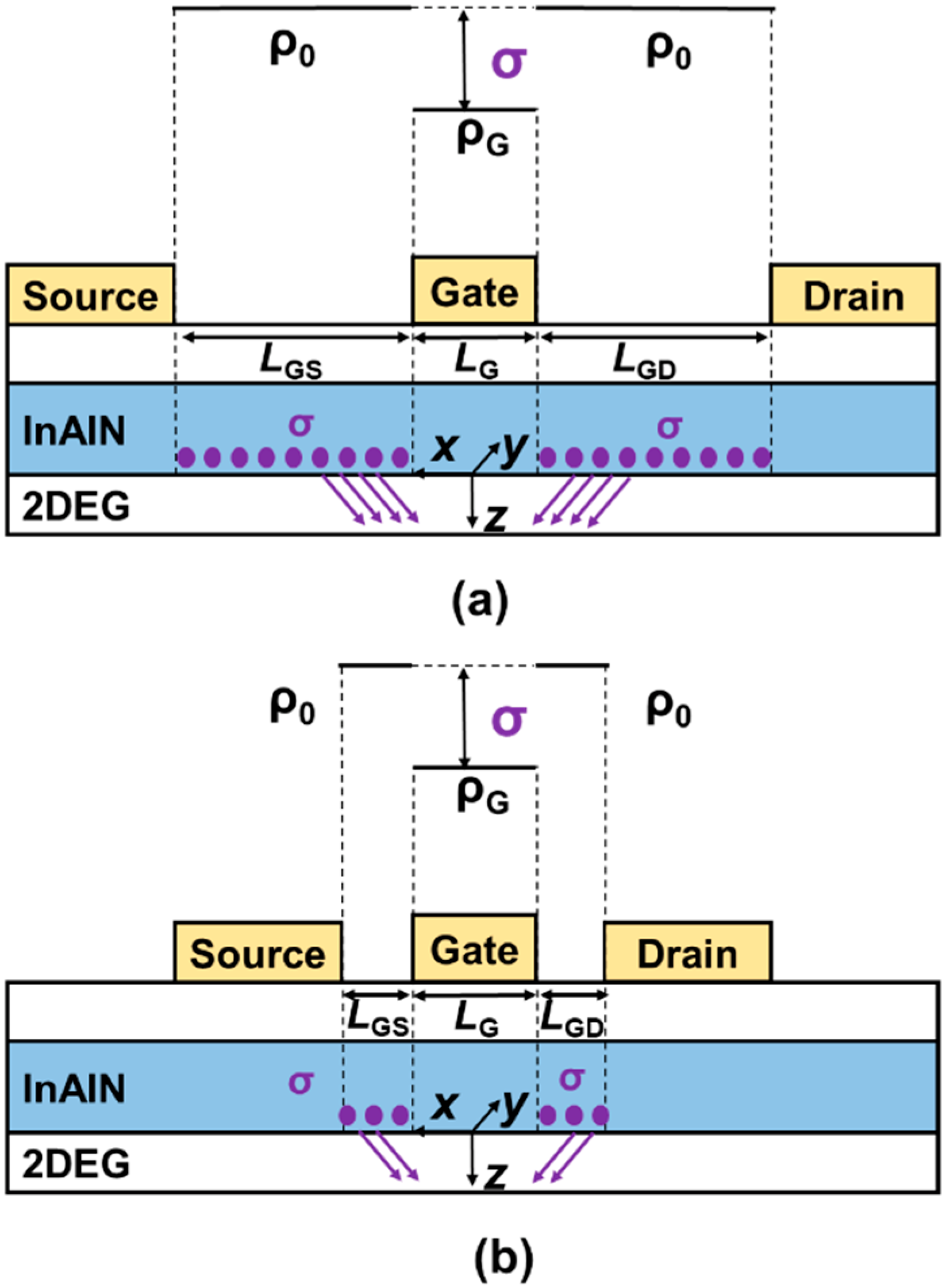
Figure 11.
Schematic of the additional polarization charge (σ) distribution in InAlN barrier with (a) large and (b) small source–drain spacing LSD. The gate length is fixed.
Figure 11.
Schematic of the additional polarization charge (σ) distribution in InAlN barrier with (a) large and (b) small source–drain spacing LSD. The gate length is fixed.

Figure 12.
(a,b) µ versus VGS for the devices with LSD of 1 µm and LG of 50, 100, 150 nm with 8 nm and 5 nm InAlN. (c,d) Calculated µPCF versus VGS of the same devices with 8 nm and 5 nm InAlN.
Figure 12.
(a,b) µ versus VGS for the devices with LSD of 1 µm and LG of 50, 100, 150 nm with 8 nm and 5 nm InAlN. (c,d) Calculated µPCF versus VGS of the same devices with 8 nm and 5 nm InAlN.

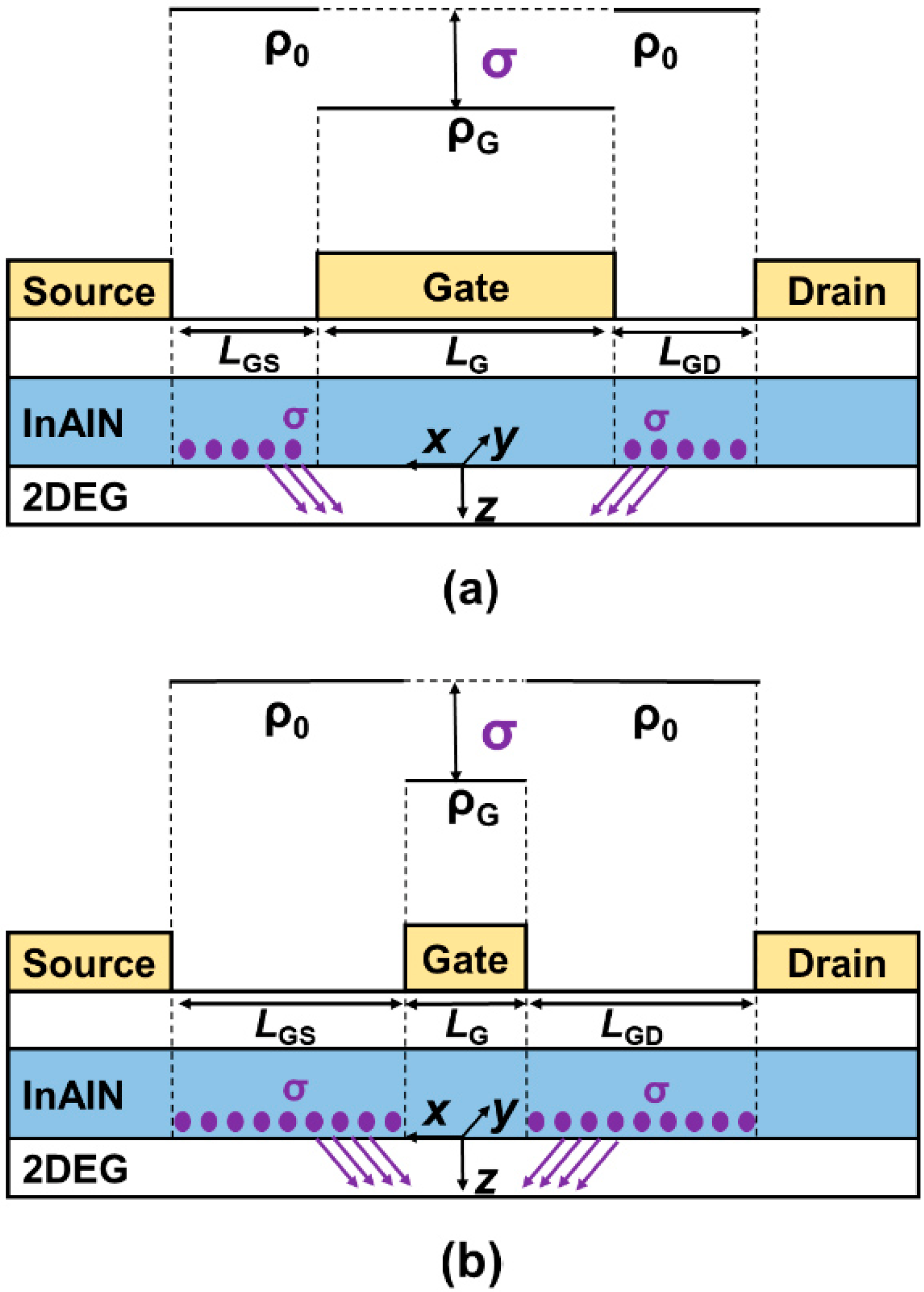
Figure 13.
Schematic of the additional polarization charge (σ) distribution in InAlN barrier with (a) large and (b) small gate length LG. The source–drain spacing LSD is fixed.
Figure 13.
Schematic of the additional polarization charge (σ) distribution in InAlN barrier with (a) large and (b) small gate length LG. The source–drain spacing LSD is fixed.

Publisher’s Note: MDPI stays neutral with regard to jurisdictional claims in published maps and institutional affiliations. |
© 2022 by the authors. Licensee MDPI, Basel, Switzerland. This article is an open access article distributed under the terms and conditions of the Creative Commons Attribution (CC BY) license (https://creativecommons.org/licenses/by/4.0/).
Share and Cite
MDPI and ACS Style
Cui, P.; Zeng, Y. Effect of Device Scaling on Electron Mobility in Nanoscale GaN HEMTs with Polarization Charge Modulation. Nanomaterials 2022, 12, 1718. https://0-doi-org.brum.beds.ac.uk/10.3390/nano12101718
AMA Style
Cui P, Zeng Y. Effect of Device Scaling on Electron Mobility in Nanoscale GaN HEMTs with Polarization Charge Modulation. Nanomaterials. 2022; 12(10):1718. https://0-doi-org.brum.beds.ac.uk/10.3390/nano12101718
Chicago/Turabian StyleCui, Peng, and Yuping Zeng. 2022. "Effect of Device Scaling on Electron Mobility in Nanoscale GaN HEMTs with Polarization Charge Modulation" Nanomaterials 12, no. 10: 1718. https://0-doi-org.brum.beds.ac.uk/10.3390/nano12101718
Note that from the first issue of 2016, this journal uses article numbers instead of page numbers. See further details here.